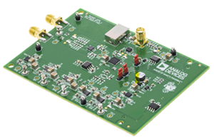
ADP5062CP-EVALZ
Analog Devices Inc.The ADP5062 charger is fully compliant with USB 3.0 and the USB Battery Charging Specification 1.2 and enables charging via the mini USB VBUS pin from a wall charger, car charger, or USB host port.The ADP5062 operates from a 4 V to 6.7 V input voltage range but is tolerant of voltages up to 20 V thereby alleviating concerns about USB bus spikes during disconnect or connect scenarios.The ADP5062 features an internal FET between the linear charger output and the battery. This permits battery isolation and, hence, system powering under a dead battery or no battery scenario, which allows for immediate system function on connection to a USB power supply.Based on the type of USB source, which is detected by an external USB detection chip, the ADP5062 can be set to apply the correct current limit for optimal charging and USB compliance.The ADP5062 has three factory-programmable digital input/out-put pins that provide maximum flexibility for different systems. These digital input/output pins permit combinations of features such as, input current limits, charging enable and disable, charging current limits, and a dedicated interrupt output pin.APPLICATIONS Digital Still Cameras Digital Video Cameras Single Cell Li-Ion Portable Equipment PDAs, Audio and GPS Devices Portable Medical Devices Mobile Phones
ADP5090-2-EVALZ
Analog Devices Inc.The ADP5090 is an integrated boost regulator that converts dc power from PV cells or TEGs. The device charges storage elements such as rechargeable Li-Ion batteries, thin film batteries, super capacitors, and conventional capacitors, and powers up small electronic devices and battery-free systems.The ADP5090 provides efficient conversion of the harvested limited power from a 16 ?W to 200 mW range with sub-?W operation losses. With the internal cold-start circuit, the regulator can start operating at an input voltage as low as 380 mV. After cold startup, the regulator is functional at an input voltage range of 80 mV to 3.3 V.By sensing the input voltage at the VIN pin, the control loop keeps the input voltage ripple in a fixed range to maintain stable dcto-dc boost conversion. The VIN OCV sensing and programmable regulation points of the input voltage allow extraction of the highest possible energy from the PV cell or TEG harvester. A programmable minimum operation threshold (MINOP) enables boost shutdown during a low light condition. In addition, the DIS_SW pin can temporarily shut down the boost regulator and is RF transmission friendly.The charging control function of ADP5090 protects rechargeable energy storage, which is achieved by monitoring the battery voltage with programmable charging termination voltage and shutdown discharging voltage. In addition, a programmable PGOOD flag monitors the SYS voltage.An optional primary cell battery can be connected and managed by an integrated power path management control block that automatically switches the power source from the energy harvester, rechargeable battery, and primary cell battery.The ADP5090 is available in a 16-lead, 3 mm ? 3 mm LFCSP and is rated for a ?40?C to +125?C junction temperature range.APPLICATIONS PV cell energy harvesting TEG energy harvesting Battery regulator powered by solar panel Industrial monitoring Self-powered wireless sensor devices Portable and wearable devices with energy harvesting
ADP5092-1-EVALZ
Analog Devices Inc.The ADP5091/ADP5092 are intelligent, integrated energy harvesting, ultralow power management unit (PMU) solutions that convert dc power from PV cells or TEGs. These devices charge storage elements such as rechargeable Li-Ion batteries, thin film batteries, super capacitors, or conventional capacitors, and power up small electronic devices and battery free systems.The ADP5091/ADP5092 provide efficient conversion of the harvested limited power from a 6 ?W to 600 mW range with submicrowatt operation losses. With the internal cold start circuit, the regulator can start operating at an input voltage as low as 380 mV. After cold startup, the regulator is functional at an input voltage range of 0.08 V to 3.3 V. An additional 150 mA regulated output can be programmed by an external resistor divider or the VID pin.The MPPT control keeps the input voltage ripple in a fixed range to maintain stable dc-to-dc boost conversion. The dynamic sensing mode and no sensing mode, both programming regulation points of the input voltage, allow extraction of the highest possible energy from the harvester. A programmable minimum operation threshold enables boost shutdown during a low input condition.As a low light indicator for a microprocessor, the LLD pin of the ADP5091 is the MINOP comparator output. However, the REG_GOOD flag of the ADP5092 monitors the REG_OUT voltage. In addition, the DIS_SW pin can temporarily shut down the boost regulator and is RF transmission friendly.The charging control function of the ADP5091/ADP5092 protects the rechargeable energy storage, which is achieved by monitoring the battery voltage with the programmable charging termination voltage and the shutdown discharging voltage. In addition, a programmable PGOOD flag monitors the SYS voltage.An optional primary cell battery can be connected and managed by an integrated power path management control block that is programmable to switch the power source from the energy harvester, rechargeable battery, and primary cell battery.The ADP5091/ADP5092 are available in a 24-lead LFCSP and are rated for a ?40?C to +125?C temperature range.Applications Photovoltaic (PV) cell energy harvesting Thermoelectric generators (TEGs) energy harvesting Industrial monitoring Self powered wireless sensor devices Portable and wearable devices with energy harvesting
ADP5134CP-EVALZ
Analog Devices Inc.The ADP5134 combines two high performance buck regulators and two low dropout (LDO) regulators. It is available in a 24-lead 4 mm ? 4 mm LFCSP.The high switching frequency of the buck regulators enables tiny multilayer external components and minimizes the board space. When the MODE pin is set to high, the buck regulators operate in forced pulse-width modulation (PWM) mode. When the MODE pin is set to low, the buck regulators operate in PWM mode when the load is above a predefined threshold. When the load current falls below a predefined threshold, the regulator operates in power save mode (PSM), improving the light load efficiency.The two buck regulators operate out of phase to reduce the input capacitor requirement. The low quiescent current, low dropout voltage, and wide input voltage range of the ADP5134 LDO regulators extend the battery life of portable devices. The ADP5134 LDO regulators maintain power supply rejection greater than 60 dB for frequencies as high as 10 kHz while operating with a low headroom voltage of 500 mV.Regulators in the ADP5134 are activated through dedicated enable pins. The default output voltages can be externally set in the adjustable version or factory programmable to a wide range of preset values in the fixed voltage version.Applications Power for processors, application specific integrated circuits (ASICs), field programmable gate arrays (FPGAs), and radio frequency (RF) chipsets Portable instrumentation and medical devices Space constrained devices
ADP5300-EVALZ
Analog Devices Inc.The ADP5300 is a high efficiency, ultralow quiescent current step-down regulator that draws only 180 nA quiescent current to regulate the output at no load.The ADP5300 runs from an input supply voltage range of 2.15 V to 6.50 V, allowing the use of multiple alkaline or NiMH, Li-Ion cells, or other power sources. The output voltage is selectable from 0.8 V to 5.0 V by an external VID resistor and factory fuse. The total solution requires only four tiny external components.The ADP5300 can operate between hysteresis mode and PWM mode via the SYNC/MODE pin. The regulator in hysteresis mode achieves excellent efficiency at a power of less than 1 mW and provides up to 50 mA of output current. The regulator in PWM mode produces a lower output ripple and supplies up to 500 mA of output current. The flexible configuration capability during operation of the device enables very efficient power management to meet both the longest battery life and low system noise requirements.The ADP5300 contains a VOUTOK flag, which monitors the output voltage and runs at a 2 MHz switching frequency in PWM mode. SYNC/MODE can be synchronized to an external clock from 1.5 MHz to 2.5 MHz.The ADP5300 includes an STOP pin that can disable the regulator switching temporarily, in this way a quiet system environment can be achieved to benefit noise sensitive circuitry, such as data conversion, RF data transmit, and analog sensors.Other key features in the ADP5300 include separate enabling, QOD, and safety features such as overcurrent protection (OCP), thermal shutdown (TSD), and input undervoltage lockout (UVLO).The ADP5300 is available in 10-lead, 3 mm ? 3 mm LFCSP rated for ?40?C to +125?C junction temperature range.Multifunction pin names may be referenced by their relevant function only.Applications Energy (gas and water) metering Portable and battery-powered equipment Medical applications Keep-alive power supplies
ADP5303-EVALZ
Analog Devices Inc.The ADP5303 is high efficiency, ultralow quiescent current step-down regulator that draws only 240 nA quiescent current to regulate the output at no load.The ADP5303 runs from an input voltage of 2.15 V to 6.50 V, allowing the use of multiple alkaline or NiMH cells, Li-Ion cells, or other power sources. The output voltage is selectable from 0.8 V to 5.0 V by an external VID resistor and a factory fuse. The total solution requires only four tiny external components.The ADP5303 can operate between hysteresis mode and PWM mode via the SYNC/MODE pin. In hysteresis mode, the regulator achieves excellent efficiency at less than 1 mW and provides up to 50 mA of output current. In PWM mode, the regulator produces a lower output ripple and supplies up to 500 mA of output current. The flexible configuration capability during operation of the device enables very efficient power management to meet both long battery life and low system noise requirements.The ADP5303 integrates an ultralow power comparator with a factory programmable voltage reference to monitor the input battery voltage. The regulator runs at a 2 MHz switching frequency in PWM mode and the SYNC/MODE pin can be synchronized to an external clock from 1.5 MHz to 2.5 MHz.Other key features in the ADP5303 include separate enabling, QOD, and safety features such as overcurrent protection (OCP), thermal shutdown (TSD), and input undervoltage lockout (UVLO).The ADP5303 is available in 9-ball, 1.65 mm ? 1.87 mm WLCSP package rated for the ?40?C to +125?C junction temperature range.Applications Energy (gas, water) metering Portable and battery-powered equipment Medical applications Keep-alive power supply
ADP7102RD-EVALZ
Analog Devices Inc.The ADP7102 is a CMOS, low dropout linear regulator that operates from 3.3 V to 20 V and provides up to 300 mA of output current. This high input voltage LDO is ideal for regulation of high performance analog and mixed signal circuits operating from 19 V to 1.22 V rails. Using an advanced proprietary architecture, it provides high power supply rejection, low noise, and achieves excellent line and load transient response with just a small 1 ?F ceramic output capacitor. The ADP7102 is available in seven fixed output voltage options and an adjustable version, which allows output voltages that range from 1.22 V to VIN ? VDO via an external feedback divider. The ADP7102 output noise voltage is 15 ?V rms and is independent of the output voltage. A digital power good output allows power system monitors to check the health of the output voltage. A user programmable precision undervoltage lockout function facilitates sequencing of multiple power supplies. The ADP7102 is available in 8-lead, 3 mm ? 3 mm LFCSP and 8-lead SOIC packages. The LFCSP offers a very compact solution and also provides excellent thermal performance for applications requiring up to 300 mA of output current in a small, low-profile footprint. APPLICATIONS Regulation to noise sensitive applications: ADC, DAC circuits, precision amplifiers, high frequency oscillators, clocks, and phase-locked loops Communications and infrastructure Medical and healthcare Industrial and instrumentation
ADP7142RD-EVALZ
Analog Devices Inc.The ADP7142 is a CMOS, low dropout (LDO) linear regulator that operates from 2.7 V to 40 V and provides up to 200 mA of output current. This high input voltage LDO is ideal for the regulation of high performance analog and mixed signal circuits operating from 39 V down to 1.2 V rails. Using an advanced proprietary architecture, the device provides high power supply rejection, low noise, and achieves excellent line and load transient response with a small 2.2 ?F ceramic output capacitor. The ADP7142 regulator output noise is 11 ?V rms independent of the output voltage for the fixed options of 5 V or less.The ADP7142 is available in 15 fixed output voltage options. The following voltages are available from stock: 1.2 V (adjustable), 1.8 V, 2.5 V, 3.3 V, 3.8 V, and 5.0 V. Additional voltages available by special order are 1.5 V, 1.85 V, 2.0 V, 2.2 V, 2.75 V, 2.8 V, 2.85 V, 3.0 V, 4.2 V, and 4.6 V.Each fixed output voltage can be adjusted above the initial set point with an external feedback divider. This allows the ADP7142 to provide an output voltage from 1.2 V to VIN ? VDO with high PSRR and low noise.User programmable soft start with an external capacitor is available in the LFCSP and SOIC packages.The ADP7142 is available in a 6-lead, 2 mm ? 2 mm LFCSP making it not only a very compact solution, but it also provides excellent thermal performance for applications requiring up to 200 mA of output current in a small, low profile footprint. The ADP7142 is also available in a 5-lead TSOT and an 8-lead SOIC.APPLICATIONS Regulation to noise sensitive applications ADC, DAC circuits, precision amplifiers, power for VCO VTUNE control Communications and infrastructure Medical and healthcare Industrial and instrumentation Automotive
ADP7156CP-3.3EVALZ
Analog Devices Inc.The ADP7156 is a linear regulator that operates from 2.3 V to 5.5 V and provides up to 1.2 A of output current. Using an advanced proprietary architecture, it provides high power supply rejection and ultralow noise, achieving excellent line and loadtransient response with only a 10 ?F ceramic output capacitor.There are 16 standard output voltages for the ADP7156. The following voltages are available from stock: 1.2 V, 1.8 V, 2.0 V, 2.5 V, 2.8 V, 3.0 V and 3.3 V. Additional voltages available by special order are 1.3 V, 1.5 V, 1.6 V, 2.2 V, 2.6 V, 2.7 V, 2.9 V, 3.1 V, and 3.2 V.The ADP7156 regulator typical output noise is 0.9 ?V rms from 100 Hz to 100 kHz and 1.7 nV/?Hz for noise spectral density from 10 kHz to 1 MHz. The ADP7156 is available in a 10-lead, 3 mm ? 3 mm LFCSP and 8-lead SOIC packages, making it not only a very compact solution, but also providing excellent thermal performance for applications requiring up to 1.2 A of output current in a small, low profile footprint.Applications Regulation to noise sensitive applications: phase-locked loops (PLLs), voltage controlled oscillators (VCOs), and PLLs with integrated VCOs Communications and infrastructure Backhaul and microwave links
ADP7159RD-04-EVALZ
Analog Devices Inc.The ADP7159 is an adjustable linear regulator that operates from 2.3 V to 5.5 V and provides up to 2 A of output current. Output voltages from 1.2 V to 3.3 V are possible depending on the model. Using an advanced proprietary architecture, the device provides high power supply rejection and ultralow noise, achieving excellentline and load transient response with only a 10 ?F ceramicoutput capacitor.The ADP7159 is available in four models that optimize powerdissipation and PSRR performance as a function of the inputand output voltage. The typical output noise of the ADP7159 regulator is 0.9 ?V rmsfrom 100 Hz to 100 kHz and 1.7 nV/?Hz for noise spectral densityfrom 10 kHz to 1 MHz. The ADP7159 is available in 10-lead,3 mm ? 3 mm LFCSP and 8-lead SOIC packages, making it notonly a very compact solution, but also providing excellent thermal performance for applications requiring up to 2 A of outputcurrent in a small, low profile footprint.Applications Regulation to noise sensitive applications: phase-locked loops (PLLs), voltage controlled oscillators (VCOs), and PLLs with integrated VCOs Communications and infrastructure Backhaul and microwave links
ADP8140CP-EVALZ
Analog Devices Inc.The ADP8140 provides high current control of up to four LED drivers. Each driver can sink up to 500 mA. The sink current is programmed for all four drivers with one external resistor.The device features a feedback output that controls an external power supply for optimal efficiency. The ADP8140 also protects the LEDs, power supply, and itself against thermal events, short circuits, overvoltages, and LED open circuits. Multiple ADP8140 ICs are easily connected in parallel to drive additional LED strings or higher current LEDs. The ADP8140 is available in a small, thermally enhanced, lead frame chip scale package (LFCSP).Applications High brightness LED lighting Large format LED backlighting
ADPA7006-EVALZ
Analog Devices Inc.The ADPA7006CHIP is a gallium arsenide (GaAs), pseudomorphic high electron mobility transistor (pHEMT), monolithic microwave integrated circuit (MMIC), distributed power amplifier that operates from 18 GHz to 44 GHz. The amplifier provides 23.5 dB of small signal gain, 29 dBm output power for 1 dB compression, and a typical output third-order intercept of 38 dBm. The ADPA7006CHIP requires 800 mA from a 5 V supply on the supply voltage (VDD), and features inputs and outputs that are internally matched to 50 ?, facilitating integration in multichip modules (MCMs). All data is taken with the chip connected via two 0.025 mm wire bonds that are less than 0.31 mm long. Applications Military and space Test instrumentation Communications
ADPA7009-EVALZ
Analog Devices Inc.The ADPA7009CHIP is a gallium arsenide (GaAs), pseudomorphic high electron mobility transistor (pHEMT), monolithic microwave integrated circuit (MMIC), 29 dBm saturated output power (0.5 W) distributed power amplifier that operates from 20 GHz to 54 GHz. The amplifier provides a gain of 19.5 dB, an output power for 1 dB compression (P1dB) of 28.5 dBm, and a typical output third-order intercept (IP3) of 35 dBm at 24 GHz to 36 GHz. The ADPA7009CHIP requires 750 mA from a 5 V supply voltage (VDD) and features inputs and outputs that are internally matched to 50 ?, facilitating integration into multichip modules (MCMs). All data is taken with the RFIN and RFOUT pads connected via one 0.076 mm (3 mil) ribbon bond of 0.076 mm (3 mil) minimal length.APPLICATIONS Military and space Test instrumentation Satellite communications
ADRF5019-EVALZ
Analog Devices Inc.The ADRF5019 is a nonreflective, single pole, double throw (SPDT) RF switch manufactured in a silicon process.The ADRF5019 operates from 100 MHz to 13 GHz with better than 0.8 dB insertion loss and 45 dB of isolation at 8 GHz. TheADRF5019 has a nonreflective design, and the RF ports are internally terminated to 50 ?.The ADRF5019 switch requires a dual supply voltage of +3.3 V and ?2.5 V and positive control voltage inputs. This switchemploys complementary metal-oxide semiconductor (CMOS)-compatible and low voltage transistor transistor logic (LVTTL)-compatible controls.The ADRF5019 can also operate with a single positive supply voltage (VDD) applied. The negative supply voltage (VSS) is tiedto ground. Even in single-supply operation mode, the ADRF5019 can cover the 100 MHz to 13 GHz operating frequency andmaintain good power handling performance. See the Applications Information section for more details.The ADRF5019 is pin-compatible with the HMC1118, the low frequency cutoff version, which operates from 9 kHz to 13.0 GHz.The ADRF5019 comes in a 16-lead, lead frame chip scale package (LFCSP) and operates from ?40?C to +105?C.Applications Test instrumentation Microwave radios and very small aperture terminals (VSATs) Military radios, radars, and electronic counter measures (ECMs) Fiber optics and broadband telecommunications
ADRF5027-EVALZ-292
Analog Devices Inc.The ADRF5027 is a nonreflective, single-pole, double-throw (SPDT) radio frequency (RF) switch manufactured in a silicon process.The ADRF5027 operates from 9 kHz to 44 GHz with better than 3.8 dB of insertion loss and 43 dB of isolation. The ADRF5027 features an all off control, where both RF ports are in an isolation state. The ADRF5027 has a nonreflective design and both of the RF ports are internally terminated to 50 ?.The ADRF5027 requires a dual-supply voltage of +3.3 V and ?3.3 V. The device employs complimentary metal-oxide semiconductor/low-voltage transistor-transistor logic (CMOS/LVTTL) logic-compatible controls.The ADRF5027 is pin compatible with the ADRF5026 fast switching version, which operates from 100 MHz to 44 GHz.The ADRF5027 RF ports are designed to match a characteristic impedance of 50 ?. For ultrawideband products, impedance matching on the RF transmission lines can further optimize high frequency insertion loss and return loss characteristics. Refer to the Narrow-Band Impedance Matching section for an example of a matched circuit that achieves a low insertion loss response of 2.2 dB from 28 GHz to 43 GHz.The ADRF5027 comes in a 20-terminal, 3 mm ? 3 mm, RoHS-compliant, land grid array (LGA) package and can operate from ?40?C to +105?C.Applications Industrial scanners Test and instrumentation Cellular infrastructure: 5G mmWave Military radios, radars, electronic counter measures (ECMs) Microwave radios and very small aperture terminals (VSATs)
ADRF5032-EVALZ
Analog Devices Inc.The ADRF5032 is a reflective, single-pole double-throw (SPDT) switch manufactured in the silicon process. The ADRF5032 operates from 1 GHz to 60 GHz with insertion loss of lower than 2.0 dB and isolation of higher than 32 dB. The device has a RF input power handling capability of 24 dBm for both through path and 21 dBm for hot switching.The ADRF5032 requires dual supply voltages of ?3.3 V. The device employs CMOS and low voltage transistor logic (LVTTL) compatible control.The ADRF5032 comes in a 12-terminal, 2.5 mm ? 2.5 mm, RoHS compliant, land grid array (LGA) package. ADRF5032 can operate from -40?C to +105?C.APPLICATIONSIndustrial scannersTest and instrumentationCellular infrastructure: 5G mmWaveMilitary radios, radars, electronic counter measures (ECMs)Microwave radios and very small aperture terminals (VSATs)
ADRF5040-EVALZ
Analog Devices Inc.The ADRF5040 is a general-purpose, broadband high isolation, nonreflective single-pole, quad-throw (SP4T) switch in an LFCSP surface-mount package. Covering the 9 kHz to 12.0 GHz range, the switch offers high isolation and low insertion loss. The switch features 34 dB isolation and 0.8 dB insertion loss up to 8.0 GHz, and a 9 ?s settling time of 0.05 dB margin of the final radio frequency output (RFOUT). The switch operates using positive control voltage of 3.3 V and 0 V and requires +3.3 V and ?3.3 V supplies. The ADRF5040 is packaged in a 4 mm ? 4 mm, surface-mount LFCSP package.Applications Test instrumentation Microwave radios and very small aperture terminals (VSATs) Military radios, radars, and electronic counter measures (ECMs) Fiber optics and broadband telecommunications?
ADRF5042-EVALZ
Analog Devices Inc.The ADRF5042 is a nonreflective SP4T switch manufactured in the silicon on insulator (SOI) process.The ADRF5042 operates from 100 MHz to 44 GHz with an insertion loss of lower than 3.2 dB and an isolation of higher than 35 dB. The device has a RF input power handling capability of 24 dBm for both through and terminated paths.The ADRF5042 requires a dual-supply voltage of +3.3 V and ?3.3 V. The device employs CMOS- and low voltage transistor to transistor logic (LVTTL)-compatible controls.The ADRF5042 has enable and logic select controls to feature all off state and port mirroring, respectively.The ADRF5042 is pin compatible with the ADRF5043 low frequency cutoff version, which operates from 9 kHz to 44 GHz.The ADRF5042 comes in a 24-terminal, 3 mm ? 3 mm, RoHS compliant, land grid array (LGA) package and can operate from ?40?C to +105?C.Applications Industrial Scanners Test instrumentation Cellular infrastructure?millimeterwave (mmWave) 5G Military radios, radars, electronic counter measures (ECMs) Microwave radios and very small aperture terminals (VSATs)
ADRF5054-EVALZ
Analog Devices Inc.The ADRF5054 is a reflective, single-pole four-throw (SP4T) switch manufactured in the silicon process.This switch operates from 100 MHz to 60 GHz with better than 3.2 dB of insertion loss and 40 dB of isolation. The ADRF5054 has an RF input power handling capability of 24 dBm for the through path.The ADRF5054 draws a low current of 150 ?A on the positive supply of +3.3 V and 520 ?A on negative supply of ?3.3 V.The device employs complementary metal-oxide semiconductor (CMOS)-/low voltage transistor to transistor logic (LVTTL)-compatible controls.The ADRF5054 RF ports are designed to match a characteristic impedance of 50 ?.The ADRF5054 comes in a 24-terminal, 3 mm ? 3 mm, RoHS compliant, land grid array (LGA) package and can operate from ?40?C to +105?C.APPLICATIONSIndustrial ScannerTest instrumentationCellular Infrastructure ? mmWave 5GMilitary radios, radars, and electronic counter measures (ECMs)Microwave radios and very small aperture terminals (VSATs)
ADRF5132-EVALZ
Analog Devices Inc.The ADRF5132 is a high power, reflective, 0.7 GHz to 5.0 GHz, silicon, single-pole, double-throw (SPDT) reflective switch in a leadless, surface-mount package. The switch is ideal for high power and cellular infrastructure applications, like long-term evolution (LTE) base stations. The ADRF5132 has high power handling of 35 dBm LTE (average typical at 105?C), a low insertion loss of 0.6 dB at 2.7 GHz, input third-order intercept of 65 dBm (typical), and 0.1 dB compression (P0.1dB) of 42.5 dBm.The on-chip circuitry operates at a single, positive supply voltage of 5 V and a typical supply current of 1.1 mA typical, making the ADRF5132 an ideal alternative to pin diode-based switches.The device is in a RoHS compliant, compact, 16-lead, 3 mm ? 3 mm LFCSP package.Applications Cellular/4G infrastructure Wireless infrastructure Military and high reliability applications Test equipment Pin diode replacement


