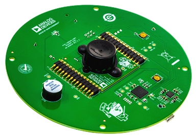
EVAL-AD7732EBZ
Analog Devices Inc.The AD7732 is a high precision, high throughput analog front end. True 16-bit peak-to-peak resolution is achievable with total conversion times of 500 ?s (2 kHz channel switching) making it ideally suitable for high resolution multiplexing applications.The part can be configured via a simple digital interface, which allows users to balance the noise performance against data throughput up to a 15.4 kHz.The analog front end features two fully differential input channels with unipolar or true bipolar input ranges to ?10 V while operating from a single +5 V analog supply. The part has an overrange and underrange detection capability and accepts an analog input overvoltage to ?16.5 V without degrading the performance of the adjacent channels.The differential reference input features ?No-Reference? detect capability. The ADC also supports per channel system calibration options. The digital serial interface can be configured for 3-wire operation and is compatible with microcontrollers and digital signal processors. All interface inputs are Schmitt triggered. The part is specified for operation over the extended industrial temperature range of ?40?C to +105?C and is available in 28-lead TSSOP package.Other parts in the AD7732 family are the AD7734?and the AD7738.The AD7734 is similar to AD7732, but its analog front end features four single-ended input channels.The AD7738 analog front end is configurable for four fully differential or eight single-ended input channels, features 0.625 V to 2.5 V bipolar/unipolar input ranges, and accepts a common-mode input voltage from 200 mV to AVDD ? 300 mV. The AD7738 multiplexer output is pinned out externally, allowing the user to implement programmable gain or signal conditioning before being applied to the ADC.APPLICATIONS PLCs/DCS Multiplexing applications Process control Industrial instrumentation
EVAL-ADCMP606BKSZ
Analog Devices Inc.The ADCMP606 and ADCMP607 are very fast comparatorsfabricated on XFCB2, an Analog Devices, Inc., proprietaryprocess. These comparators are exceptionally versatile and easyto use. Features include an input range from VEE ? 0.5 V toVCCI + 0.2 V, low noise, CML-compatible output drivers, andTTL-/CMOS-compatible latch inputs with adjustable hysteresisand/or shutdown inputs.The devices offer 1.25 ns propagation delay with 2.5 ps rmsrandom jitter (RJ). Overdrive and slew rate dispersion aretypically less than 50 ps.A flexible power supply scheme allows the devices to operatewith a single +2.5 V positive supply and a ?0.5 V to +2.7 Vinput signal range up to a +5.5 V positive supply with a ?0.5 Vto +5.7 V input signal range. The ADCMP607 features splitinput/output supplies with no sequencing restrictions tosupport a wide input signal range with independent outputswing control and power savings.The CML-compatible output stage is fully back-matched forsuperior performance. The comparator input stage offers robustprotection against large input overdrive, and the outputs do notphase reverse when the valid input signal range is exceeded. Onthe ADCMP607, latch and programmable hysteresis features arealso provided with a unique single-pin control option.The ADCMP606 is available in a 6-lead SC70 package and theADCMP607 is available in a 12-lead LFCSP package.Applications High speed instrumentation Clock and data signal restoration Logic level shifting or translation Pulse spectroscopy High speed line receivers Threshold detection Peak and zero-crossing detectors High speed trigger circuitry Pulse-width modulators Current-/voltage-controlled oscillators Automatic test equipment (ATE)
EVAL-AD7705EBZ
Analog Devices Inc.The AD7705 / AD7706?are complete analog front ends for low frequency measurement applications. These 2-/3-channel devices can accept low level input signals directly from a transducer and produce serial digital output. The devices employ a ?-? conversion technique to realize up to 16 bits of no missing codes performance. The selected input signal is applied to a proprietary, programmable-gain front end based around an analog modulator. The modulator output is processed by an on-chip digital filter. The first notch of this digital filter can be programmed via an on-chip control register, allowing adjustment of the filter cutoff and output update rate. The AD7705 / AD7706 devices operate from a single 2.7 V to 3.3 V or 4.75 V to 5.25 V supply. The AD7705 features two fully differential analog input channels; the AD7706 features three pseudo differential input channels. Both devices feature a differential reference input. Input signal ranges of 0 mV to 20 mV through 0 V to 2.5 V can be incorporated on both devices when operating with a VDD of 5 V and a reference of 2.5 V. They can also handle bipolar input signal ranges of ?20 mV through ?2.5 V, which are referenced to the AIN(?) inputs on the AD7705 and to the COMMON input on the AD7706.The AD7705 / AD7706 devices, with a 3 V supply and a 1.225 V reference, can handle unipolar input signal ranges of 0 mV to 10 mV through 0 V to 1.225 V. The devices can accept bipolar input ranges of ?10 mV through ?1.225 V. Therefore, the AD7705 / AD7706 devices perform all signal conditioning and conversion for a 2-channel or 3-channel system. The AD7705 / AD7706 are ideal for use in smart, microcontroller, or DSP-based systems. The devices feature a serial interface that can be configured for 3-wire operation. Gain settings, signal polarity, and update rate selection can be configured in software using the input serial port. The parts contains self-calibration and system calibration options to eliminate gain and offset errors on the part itself or in the system. CMOS construction ensures very low power dissipation, and the power-down mode reduces the standby power consumption to 20 ?W typ. These parts are available in a 16-lead, wide body (0.3 inch), plastic dual in-line package (DIP); a 16-lead, wide body (0.3 inch), standard small outline (SOIC) package; and a low profile, 16-lead, thin shrink small outline package (TSSOP).
EVAL-ADCMP607BCPZ
Analog Devices Inc.The ADCMP606 and ADCMP607 are very fast comparatorsfabricated on XFCB2, an Analog Devices, Inc., proprietaryprocess. These comparators are exceptionally versatile and easyto use. Features include an input range from VEE ? 0.5 V toVCCI + 0.2 V, low noise, CML-compatible output drivers, andTTL-/CMOS-compatible latch inputs with adjustable hysteresisand/or shutdown inputs.The devices offer 1.25 ns propagation delay with 2.5 ps rmsrandom jitter (RJ). Overdrive and slew rate dispersion aretypically less than 50 ps.A flexible power supply scheme allows the devices to operatewith a single +2.5 V positive supply and a ?0.5 V to +2.7 Vinput signal range up to a +5.5 V positive supply with a ?0.5 Vto +5.7 V input signal range. The ADCMP607 features splitinput/output supplies with no sequencing restrictions tosupport a wide input signal range with independent outputswing control and power savings.The CML-compatible output stage is fully back-matched forsuperior performance. The comparator input stage offers robustprotection against large input overdrive, and the outputs do notphase reverse when the valid input signal range is exceeded. Onthe ADCMP607, latch and programmable hysteresis features arealso provided with a unique single-pin control option.The ADCMP606 is available in a 6-lead SC70 package and theADCMP607 is available in a 12-lead LFCSP package.Applications High speed instrumentation Clock and data signal restoration Logic level shifting or translation Pulse spectroscopy High speed line receivers Threshold detection Peak and zero-crossing detectors High speed trigger circuitry Pulse-width modulators Current-/voltage-controlled oscillators Automatic test equipment (ATE)
LTM4681 Demo Board | PolyPhase Single Output Step-Down µModule Regulator with Digital PSM: 4 × LTM4681 at 480A
Analog Devices Inc.Demonstration circuit DC3082A-C features the LTM4681: the wide input and output voltage range, high efficiency and power density, high current PolyPhase® single output DC/DC step-down μModule® regulator with digital power system management. DC3082A-C is configured as 16-phase single output using 4× LTM4681. The factory default input voltage is 12V typical, output voltage is 1V at 480A typical or 500A peak with recommended 400LFM forced airflow. The demo board output voltages can be adjusted from 0.6V to 1V. Programming the output voltages to any value that is greater than 1V, requires derating output current based on thermal derating curves provided in the data sheet of the LTM4681. Heat sink or other appropriate electronic cooling systems can also be used in conjunction with forced airflow to further optimize the output power when the output is on and loaded with maximum output current. The factory default switching frequency is preset at 350kHz typical. DC3082A-C comes with PMBus interface and digital power system management functions. An onboard 12-pin connector is available for users to connect the dongle DC1613A to the demo board, provides an easy way to communicate and program the part using LTpowerPlay® software development tool. LTpowerPlay software and I2C/PMBus/SMBus dongle DC1613A allows users to monitor real time telemetry of input and output voltages, input and output current, switching frequency, internal IC die temperatures, power stage component temperatures and fault logs. Programmable parameters include device address, output voltages, control loop compensation, switching frequency, phase interleaving, DCM or CCM mode of operation, digital soft-start, sequencing and time based shutdown, fault responses to input and output overvoltage, output overcurrent, IC die and power component overtemperature.
The LTM4681 is available in a thermally enhanced, low profile 330-Lead (15mm × 22mm × 8.17mm) BGA package. It is recommended to read the data sheet and the demo manual of LTM4681 prior to use or making any hardware changes to DC3082A-C.
LTpowerPlay software can be downloaded here.
USB to PMBus Controller Dongle DC1613A for use with LTpowerPlay is available here.
EV-ADF5902SD1Z
Analog Devices Inc.The ADF5902 is a 24 GHz transmitter (Tx) monolithic microwaveintegrated circuit (MMIC) with an on-chip, 24 GHz voltagecontrolled oscillator (VCO). The VCO features a fractional-Nfrequency synthesizer with waveform generation capability withprogrammable grid array (PGA) and dual transmitter channelsfor radar systems. The on-chip, 24 GHz VCO generates the24 GHz signal for the two transmitter channels and the localoscillator (LO) output. Each transmitter channel contains apower control circuit. There is also an on-chip temperaturesensor.Control of all the on-chip registers is through a simple, 4-wireserial peripheral interface (SPI).The ADF5902 comes in a compact, 32-lead, 5 mm ? 5 mmLFCSP package. Applications Automotive radars Industrial radars Microwave radar sensors
LT1937ESC6 | 2-Ckt, High Efficiency Constant-Current Single Cell Li-Ion White LED (4) Driver with On-Board Battery
Analog Devices Inc.DC507A: Demo Board for the LT1937 White LED Step-Up Converter in SC70 and ThinSOT.
AD8224-EVALZ
Analog Devices Inc.The AD8224 is the first single-supply, JFET input instrumentation amplifier available in the space-saving 16-lead, 4 mm ? 4 mm LFCSP. It requires the same board area as a typical single instrumentation amplifier yet doubles the channel density and offers a lower cost per channel without compromising performance.Designed to meet the needs of high performance, portable instrumentation, the AD8224 has a minimum common-mode rejection ratio (CMRR) of 86 dB at dc and a minimum CMRR of 80 dB at 10 kHz for G = 1. Maximum input bias current is 10 pA and typically remains below 300 pA over the entire industrial temperature range. Despite the JFET inputs, the AD8224 typically has a noise corner of only 10 Hz.With the proliferation of mixed-signal processing, the number of power supplies required in each system has grown.Designed to alleviate this problem, the AD8224 can operate on a ?18 V dual supply, as well as on a single +5 V supply. The device?s rail-to-rail output stage maximizes dynamic range on the low voltage supplies common in portable applications. Its ability to run on a single 5 V supply eliminates the need for higher voltage, dual supplies. The AD8224 draws 750 ?A of quiescent current per amplifier, making it ideal for battery powered devices.In addition, the AD8224 can be configured as a single-channel, differential output, instrumentation amplifier. Differential outputs provide high noise immunity, which can be useful when the output signal must travel through a noisy environment, such as with remote sensors. The configuration can also be used to drive differential input ADCs.For a single-channel version, use the AD8220.Applications Medical instrumentation Precision data acquisition Transducer interfaces Differential drives for high resolution input ADCs Remote sensors
EVAL-AD7147EBZ
Analog Devices Inc.The AD7147 CapTouch? controller is designed for use with capacitance sensors implementing functions such as buttons, scroll bars, and wheels. The sensors need only one PCB layer, enabling ultrathin applications.The AD7147 is an integrated CDC with on-chip environmental calibration. The CDC has 13 inputs channeled through a switch matrix to a 16-bit, 250 kHz sigma-delta (?-?) converter. The CDC is capable of sensing changes in the capacitance of the external sensors and uses this information to register a sensor activation. By programming the registers, the user has full control over the CDC setup.High resolution sensors require minor software to run on the host processor.The AD7147 is designed for single electrode capacitance sensors (grounded sensors). There is an active shield output to minimize noise pickup in the sensor.The AD7147 has on-chip calibration logic to compensate for changes in the ambient environment. The calibration sequence is performed automatically and at continuous intervals as long as the sensors are not touched. This ensures that there are no false or non-registering touches on the external sensors due to a changing environment.The AD7147 has an SPI-compatible serial interface, and the AD7147-1 has an I2C?-compatible serial interface. Both parts have an interrupt output, as well as a GPIO. There is a VDRIVE pin to set the voltage level for the serial interface independent of VCC.The AD7147 is available in a 24-lead, 4 mm ? 4 mm LFCSP and operates from a 2.6 V to 3.6 V supply. The operating current consumption in low power mode is typically 26 ?A for 13 sensors.APPLICATIONS Cell phones Personal music and multimedia players Smart handheld devices Television, A/V, and remote controls Gaming consoles Digital still cameras?
DC2199A-B
Analog Devices Inc.The LTC3766 is a PolyPhase-capable secondary-side controller for synchronous forward converters. When used in conjunction with the LTC3765 active-clamp forward controller and gate driver, the part creates a complete isolated power supply that combines the power of multiphase operation with the speed of secondary-side control.The LTC3766 has been designed to simplify the design of active clamp forward converters. Working in concert with the LTC3765, the LTC3766 forms a robust, self-starting converter that eliminates the need for the separate bias regulator that is commonly used in secondary-side control applications. A precision current-limit coupled with clean start-up into a pre-biased load make the LTC3766 an excellent choice for high-power battery charger applications.The LTC3766 provides extensive remote sensing and output protection features, while Direct Flux Limit guarantees no transformer saturation without compromising transient response. A linear regulator controller and internal bypass LDO are also provided to simplify the generation of the secondary-side bias voltage.Applications Isolated 48V Telecommunication Systems Isolated Battery Chargers Automotive and Military Systems Industrial, Avionics and Heavy Equipment
AD9083EBZ
Analog Devices Inc.The AD9083 is a 16-channel, 125 MHz bandwidth, continuous time ?-? (CTSD) ADC. The device features an on-chip, programmable, single-pole antialiasing filter and termination resistor that is designed for low power, small size, and ease of use. The 16 ADC cores features a first-order, CTSD modulator architecture with integrated, background nonlinearity correction logic and self cancelling dither. Each ADC features wide bandwidth inputs supporting a variety of user-selectable input ranges. An integrated voltage reference eases design considerations. The analog input and clock signals are differential inputs. Each ADC has a signal processing tile to filter out of band shaped noise from the ?-? ADC and reduce the sample rate. Each tile contains a cascaded integrator comb (CIC) filter, a quadrature digital downconverter (DDC) with multiple finite input response (FIR) decimation filters (decimate by J block), or up to three quadrature DDC channels with averaging decimation filters for data gating applications. Users can configure the Subclass 1 JESD204B based, high speed serialized output in a variety of lane configurations (up to four), depending on the DDC configuration and the acceptable lane rate of the receiving logic device. Multiple device synchronization is supported through the SYSREF?, TRIG?, and SYNCINB? input pins. The AD9083 has flexible power-down options that allow significant power savings when desired. All of these features can be programmed using a 1.8 V capable 3-wire serial port interface (SPI). The AD9083 is available in a Pb-free, 100-ball CSP_BGA and is specified over the ?40?C to +85?C industrial temperature range.This product is protected by a US patent.APPLICATIONS Millimeter wave imaging Electronic beam forming and phased arrays Multichannel wideband receivers Electronic support measuresPRODUCT HIGHLIGHTS Continuous time, ?-? analog-to-digital converters (ADCs) support signal bandwidths of up to 125 MHz with low power and minimal filtering. Integrated digital processing blocks reduce data payload and lower overall system cost. Configurable JESD204B interface reduces printed circuit board (PCB) complexity. Flexible power-down options. SPI interface controls various product features and functions to meet specific system requirements. Small, 9 mm ? 9 mm, 100-ball CSP_BGA package, simple interface, and integrated digital processing save PCB space.
LTC1628CG-PG | High Efficiency, Multi-Phase 2-Output, Current Mode Controller, 5-30 VIN, 5V/4A and 3.3V/4A Output
Analog Devices Inc.DC236C-C: Demo Board for the LTC1628 High Efficiency, 2-Phase Synchronous Step-Down Switching Regulator.
EVAL-ADXL362Z
Analog Devices Inc.The ADXL362 is an ultralow power, 3-axis MEMS accelerometer that consumes less than 2 ?A at a 100 Hz output data rate and 270 nA when in motion triggered wake-up mode. Unlike accelerometers that use power duty cycling to achieve low power consumption, the ADXL362 does not alias input signals by undersampling; it samples the full bandwidth of the sensor at all data rates.The ADXL362 always provides 12-bit output resolution; 8-bit formatted data is also provided for more efficient single-byte transfers when a lower resolution is sufficient. Measurement ranges of ?2 g, ?4 g, and ?8 g are available, with a resolution of 1 mg/LSB on the ?2 g range. For applications where a noise level lower than the normal 550 ?g/?Hz of the ADXL362 is desired, either of two lower noise modes (down to 175 ?g/?Hz typical) can be selected at minimal increase in supply current.In addition to its ultralow power consumption, the ADXL362 has many features to enable true system level power reduction. It includes a deep multimode output FIFO, a built-in micropower temperature sensor, and several activity detection modes including adjustable threshold sleep and wake-up operation that can run as low as 270 nA at a 6 Hz (approximate) measurement rate. A pin output is provided to directly control an external switch when activity is detected, if desired. In addition, the ADXL362 has provisions for external control of sampling time and/or an external clock.The ADXL362 operates on a wide 1.6 V to 3.5 V supply range, and can interface, if necessary, to a host operating on a separate, lower supply voltage. The ADXL362 is available in a 3 mm ? 3.25 mm ? 1.06 mm package.APPLICATIONS Hearing aids Home healthcare devices Motion enabled power save switches Wireless sensors Motion enabled metering devices
EV1HMC1019ALP4
Analog Devices Inc.The HMC1019ALP4E is a broadband 5-bit GaAs IC digital attenuator in a low cost leadless surface mount package. Covering 0.1 to 30.0 GHz, the insertion loss is less than 4.0 dB typical. The attenuator bit values are 0.5 (LS B), 1, 2, 4, 8 for a total attenuation of 15.5 dB. Attenuation accuracy is excellent at ?0.3 dB typical step error with an IIP3 of +45 dBm. The control interface is CMOS/TTL compatible and accepts a three wire serial input. The HMC1019ALP4E features a user selectable power up state and a serial output port for cascading other Analog Devices serial controlled components.APPLICATIONS Fiber Optics & Broadband Telecom Microwave Radio & VSAT Military Radios, Radar & ECM Space Applications Sensors Test & Measurement Equipment
EVAL-AD5144DBZ
Analog Devices Inc.The AD5124/AD5144/AD5144A potentiometers provide a nonvolatile solution for 128-/256-position adjustment applications, offering guaranteed low resistor tolerance errors of ?8% and up to ?6 mA current density in the Ax, Bx, and Wx pins.The low resistor tolerance and low nominal temperature coefficientsimplify open-loop applications as well as applications requiringtolerance matching.The linear gain setting mode allows independent programmingof the resistance between the digital potentiometer terminals, through the RAW and RWB string resistors, allowing very accurate resistor matching.The high bandwidth and low total harmonic distortion (THD)ensure optimal performance for ac signals, making these devicessuitable for filter design.The low wiper resistance of only 40 ? at the ends of the resistor array allow for pin-to-pin connection.The wiper values can be set through an SPI-/I2C-compatible digital interface that is also used to read back the wiper register andEEPROM contents.The AD5124/AD5144/AD5144A are available in a compact, 24-lead, 4 mm ? 4 mm LFCSP and a 20-lead TSSOP. The partsare guaranteed to operate over the extended industrial temperaturerange of ?40?C to +125?C.APPLICATIONS Portable electronics level adjustment LCD panel brightness and contrast controls Programmable filters, delays, and time constants Programmable power suppliesThe AD5144-EP supports defense and aerospace applications (AQEC).
DC1110A
Analog Devices Inc.The LTC2751 is a family of 12-, 14-, and 16-bit multiplying parallel-input, current-output DACs. They operate from a single 2.7V to 5.5V supply. All parts are guaranteed monotonic over temperature. The LTC2751A-16 provides 16-bit performance (?1LSB INL and DNL) overtemperature without any adjustments. These SoftSpan? DACs offer six output ranges ? two unipolar and four bipolar ? that can be programmed through the parallel interface, or pin strapped for operation in a single range.These parts use a bidirectional input/output parallel interface that allows read back of any on-chip register. A power-on circuit resets the DAC output to 0V when power is initially applied. A logic low on the CLR pin asynchronously clears the DAC to 0V in any output range. The parts are specified over commercial and industrial temperature ranges.Applications High Resolution Offset and Gain Adjustment Process Control and Industrial Automation Automatic Test Equipment Data Acquisition Systems
EVAL-ADE1201EBZ
Analog Devices Inc.The ADE12011 is a single channel, configurable, isolated?digital input monitoring solution for energy transmission and?distribution applications. The ADE1201 is configured through?the serial port interface (SPI) to perform an isolated measurement?of the digital input that is also called binary input or contact?input. The ADE1201 digital output signal on the DOUT1 pin?reflects the state of the input signal after user configurable?signal conditioning. The SPI protocol supports addressing to?allow up to eight devices sharing one 4-wire SPI port.The ADE1201 application circuit accepts a wide range of input?voltages from ?10 V dc to ?300 V dc, or 8 V rms to 240 V rms.?The programmable wetting current and robust application?circuit enable the device to meet stringent, system level?electromagnetic capability (EMC) requirements.The ADE1201 includes an isoPower? integrated, isolated dc-to-dc?converter that eliminates the need for an external isolated power?supply. The iCoupler? chip scale transformer technology is?used to isolate the logic signals between the high voltage,?isolated side and the low voltage, nonisolated side of the?digital input monitor. This technology creates a small form?factor design that includes data and power isolation.An integrated successive approximation register (SAR)?analog-to-digital converter (ADC) and a programmable gain?amplifier (PGA) from 1? to 10? measure the analog inputs.?The ADC waveforms are available through the SPI port to?allow system level diagnostics.Product Highlights Single channel, configurable, isolated digital input. Single hardware design supports 24 V to 300 V systems. Robust architecture. Enables system level diagnostics.Applications Energy transmission and distribution Multifunction relay protection Substation battery monitoring Bay or substation interlocking Merge unit Circuit breaker status indication Remote terminal unit Building automation1 Protected by U.S. Patent Number 2017/0250043. Other patents pending.
DC540A-A
Analog Devices Inc.The LTC1604 is a 333ksps, 16-bit sampling A/D converter that draws only 220mW from ?5V supplies. This high performance device includes a high dynamic range sample-and-hold, a precision reference and a high speed parallel output. Two digitally selectable power shutdown modes provide power savings for low power systems.The LTC1604's full-scale input range is ?2.5V. Outstanding AC performance includes 90dB S/(N+D) and ?100dB THD at a sample rate of 333ksps.The unique differential input sample-and-hold can acquire single-ended or differential input signals up to its 15MHz bandwidth. The 68dB common mode rejection allows users to eliminate ground loops and common mode noise by measuring signals differentially from the source.The ADC has ?P compatible,16-bit parallel output port. There is no pipeline delay in conversion results. A separate convert start input and a data ready signal (BUSY) ease connections to FlFOs, DSPs and microprocessors.Applications Telecommunications Digital Signal Processing Multiplexed Data Acquisition Systems High Speed Data Acquisition Spectrum Analysis Imaging Systems
LT1725CGN | Isolated Forward Converter, VIN=36V to 72V, VOUT=3.3V@30A
Analog Devices Inc.DC562A-A: Demo Board for the LT1725 General Purpose Isolated Flyback Controller.
LT1725CGN | Isolated Forward Converter, VIN=36V to 72V, VOUT=12V@12A
Analog Devices Inc.DC562A-C: Demo Board for the LT1725 General Purpose Isolated Flyback Controller.


