
LT4293, LT4321 IEEE 802.3bt and LTPoE++ Interoperable Powered Device
Analog Devices Inc.Demonstration circuit 2911A is an IEEE 802.3bt compliant and LTPoE++ interoperable Power over Ethernet (PoE) Powered Device (PD). It features the LT4293 PD interface controller and the LT4321 PoE ideal diode bridge controller.
The LT4293 provides LTPoE++, IEEE 802.3af (PoE, Type 1), IEEE 802.3at (PoE+, Type 2), and IEEE 802.3bt (PoE++, Type 3 and 4) compliant interfacing. It utilizes an external, low RDS(ON) (30mΩ typical) N-channel MOSFET for the Hot Swap function to improve efficiency.
Power good (PWRGD) output indicates the PD controller is ready to provide power to the downstream load. This signal can be used to enable an isolated power supply. The T2P output indicates the available power from the Power Sourcing Equipment (PSE). This signal communicates allocated power from either LTPoE++ or IEEE 802.3bt-compliant PSEs to the downstream PD circuitry.
The LT4321 controls eight low RDS(ON) (57mΩ typical) N-channel MOSFETs to further improve end-to-end power delivery efficiency and ease thermal design. This solution replaces the eight diodes typically found in a passive PoE rectifier bridge.
The DC2911A accepts up to 90W of delivered power from a PSE via the RJ45 connector (J1) or a local 48V DC power supply using the auxiliary supply input. When both supplies are connected, the auxiliary supply input has priority over the PoE input.

LTC5597 | 100MHz to 70GHz RMS Power Detector
Analog Devices Inc.Demonstration circuit 2932A hosts a high accuracy RMS power detector featuring the LTC5597 IC. This ultrawide bandwidth device has a RMS response that measures RF and microwave signals from 100MHz to 70GHz. The input signal converts to a DC voltage that is logarithmically proportional to the input signal level. Moreover, the LTC5597 offers unprecedented sensitivity, capable of detecting signals of –37dBm typical. Additionally, it has outstanding input dynamic range up to 35dB, achieving 1dB accuracy, depending on frequency. The detector output voltage slope is normally 29mV/dB. The PCB layout employs the recommended microstrip transmission line structure, as well as the recommended endpoint transitions. Input impedance to LTC5597 is internally matched to 50Ω. It is suitable for RMS measurements of high crest factor waveforms up to 12dB peak/average ratio. No external coupling capacitor is necessary if DC voltage at RFIN pin is kept below 1V. Contact applications support for more information.

LT8357 Demo Board | Low IQ High Power Boost Converter
Analog Devices Inc.Demonstration circuit 2937A features the LT8357 as a 360kHz low IQ, high power boost converter with a 48V output from 10V to 40V input. This demonstration circuit
features spread spectrum frequency modulation (SSFM) and split gate driver pins for the high power, high voltage switch. The converter can output 2A and higher (see Figure 3 in the demo manual). When placed in shutdown, the converter has very low quiescent current, ideal in automotive and other battery-powered applications. Low quiescent current can be achieved with both pulse-skipping and Burst Mode® operation as jumper selections on this demonstration circuit.
The LT8357 boost controller IC operates over an input range of 3V to 60V, suitable for automotive, telecom and industrial applications. It also exhibits a low quiescent
current of 8μA, making it ideal for battery-operated systems. It drives a low side N-channel power MOSFET with a 5V split gate drive. The controller provides adjustable
and synchronizable operation from 100kHz to 2MHz. At light load, either pulse-skipping or low-ripple Burst Mode operation can be selected to improve the efficiency.
It also packs many popular features such as soft-start, input undervoltage lockout, adjustable frequency and clock synchronization. PGOOD indicates when the output
voltage is in regulation.
The LT8357 comes in a thermally enhanced 12-lead plastic MSE package. The LT8357 data sheet gives a complete description of the part, pins, features, operation and
application information. The data sheet must be read in conjunction with the demo manual for DC2937A.

DC2945A
Analog Devices Inc.The LTC4246 contains eight switches, each with an independent circuit breaker function. It is particularly well suited for extremely space constrained designs. Each switch can operate completely autonomously or be arbitrarily grouped with other switches that will respond together to the fault of any single device within its group. Optionally, channel grouping may be extended to multiple LTC4246 devices by selecting the FIN# (fault input) pin as part of a channel group. A required bias supply between 2.5V to 5V allows the switches to independently operate from 13.2V down to 0V. The LTC4246 provides an SPI serial interface to enable, disable and configure the timing and current thresholds of each channel as well as provide status to each channel?s fault state.A common open-drain FAULT status output indicates if any switch has opened due to a circuit breaker event.APPLICATIONSATE Wafer Probe ElectronicsScope Probe ProtectionIndustrial ControlRelay Replacement

DC2951A
Analog Devices Inc.The LTC7806 is a high performance 2-phase single output synchronous boost converter controller that drives two N-channel power MOSFET stages out-of-phase. Its constant-frequency current mode architecture allows a phase-lockable switching frequency of up to 3MHz. High frequency 2-phase operation reduces input and output capacitor requirements and allows the use of smaller inductors compared to the single-phase equivalent. Synchronous rectification increases efficiency, reduces power losses, and eases thermal requirements, simplifying high power boost applications. The synchronous PassThru capability also minimizes losses in automotive start-stop applications.The LTC7806 operates from a wide 4.5V to 40V input supply range. When biased from the boost converter output, the LTC7806 can operate from an input supply as low as 1V after start-up. The very low no-load quiescent current extends operating run time in battery powered systems. OPTI-LOOP? compensation allows the transient response to be optimized over a wide range of output capacitance and ESR values. The LTC7806 features a precision 1.2V reference, a power good output indicator, and an inductor current monitor.APPLICATIONS Automotive and Transportation Audio and RF Power Amplifiers Industrial and Medical Communications

DC2966A
Analog Devices Inc.The LTC3376 is a highly flexible multioutput power supply IC. The device includes four synchronous buck converters, configured to share eight 1.5A power stages, powered from independent 3V to 20V inputs. The DC/DCs are assigned to one of fifteen power configurations via pin strappable CFG0 to CFG3 pins. The LTC3376 includes the integration of ceramic capacitors into the package for the BST pins thereby saving PCB space. The common buck switching frequency may be programmed with an external resistor, synchronized to an external oscillator, or set to a default internal 2MHz clock. The operating mode for all DC/DCs may be programmed via the SYNC/MODE pin for Burst Mode or forced continuous mode operation. The PGOOD1 to PGOOD4 outputs indicate when each enabled DC/DC is within a specified percentage of its final output. Current monitors allow for external monitoring of each buck?s load. The EXTVCC pin allows for the internal circuitry to run from a 3V to 5.5V rail for improved efficiency. Precision RUN pin thresholds facilitate power-up sequencing. The LTC3376 is available in a 64 lead 7mm ? 7mm BGA (0.8mm ball pitch).Applications? Telecom/Industrial? 12V Distributed Power Systems

DC2969A-A
Analog Devices Inc.The LTC4372/LTC4373 are positive high voltage ideal diode controllers that drive an external N-channel MOSFET to replace a Schottky diode. They control the forward voltage drop across the MOSFET to ensure current delivery or current transfer from one path to the other even at light loads.A 5?A operating current achieves high efficiency for intermittent load applications or always-on backup power supplies. If a power source fails or is shorted, a fast turn-off minimizes reverse current transients. The LTC4372/LTC4373 control back-to-back N-channel MOSFETs for inrush current control and load switching.The LTC4372?s SHDN pin keeps the MOSFET off and reduces the quiescent current to 3.5?A. The LTC4373 has a UV pin for undervoltage monitoring while the UVOUT?pin provides hysteresis adjustment and status information. During undervoltage, the back-to-back MOSFETs are cut off and quiescent current reduces to 0.5?A.APPLICATIONS Automotive Battery Protection Redundant Power Supplies Portable Instrumentation Solar Powered Systems Energy Harvesting Applications Supply Holdup

LTC3337 | Primary Battery SOH Monitor with Precision Coulomb Counter
Analog Devices Inc.Demonstration circuit 2973A shows the LTC3337 Primary Battery State of Health (SOH) monitor with precision coulomb counter operating with a configurable peak current limit. The LTC3337 supports input voltages from 1.8V to 5.5V and a peak current up to 100mA with a quiescent current of 100nA. Coulomb count, battery voltage, and Battery Series Resistance (BSR) are measurable and can be used to quantify the charge state and health of a battery.
The DC2973A demonstrates a simple layout for the highest-power configuration of the LTC3337. The circuit can be reduced for lower IPEAK levels. The demo board can be connected directly to a PC using a micro USB cable in order to run a GUI and configure simple a Battery State of Charge (SOC) monitor. Source code for the GUI is available and can be used as a starting point for LTC3337 firmware development.
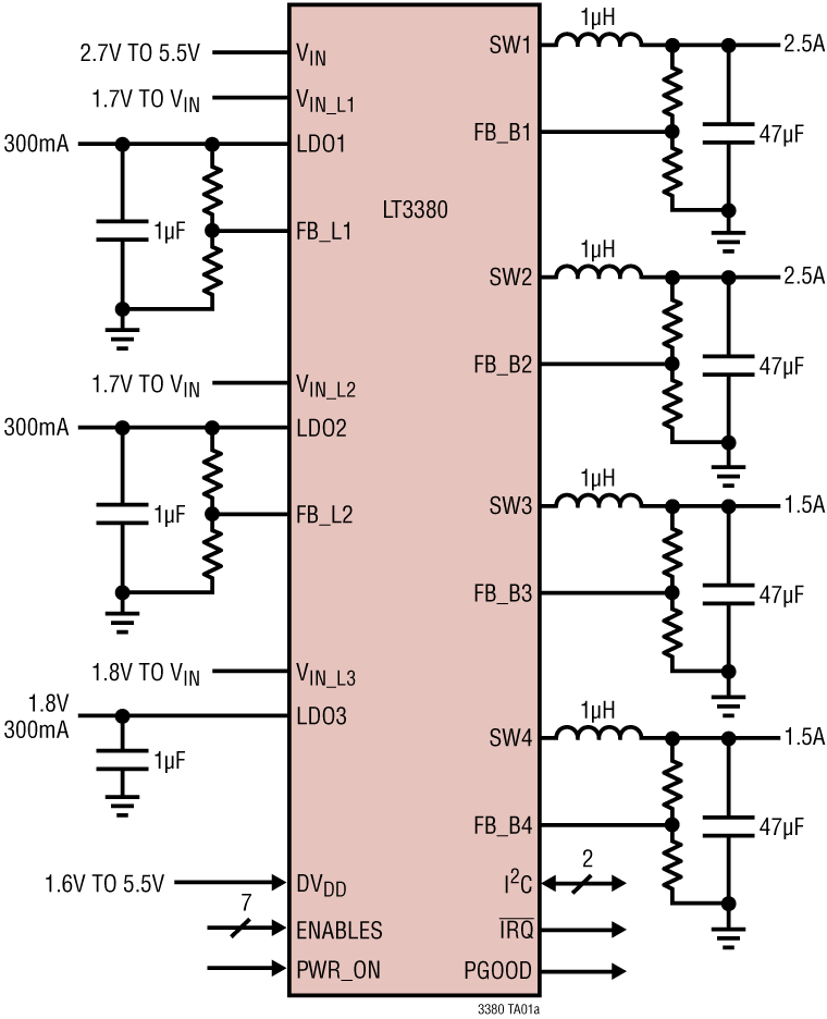
LT3380 Demo Board | Multi-Output Power Management Solution with 4 Buck Switching and 3 LDO Linear Regulators with I2C
Analog Devices Inc.DC2985A is a multi-output power management solution demonstration circuit, featuring the LT3380. It contains two 2.5A, two 1.5A synchronous step-down DC/DC regulators and three 300mA LDO regulators.
All regulators can be enabled with external enable pins. After the first regulator is enabled, the remaining enable pins use a precision threshold to allow hardwire-programmed Power-Up Sequence.
A micro-USB communication interface is integrated on board to allow software GUI to write or read the registers in LT3380 via its I2C serial port. This GUI can control regulator enables, power-down sequencing, output voltage levels, dynamic voltage scaling, operation modes, status reporting and other special functions.
Refer to LT3380 data sheet for more details on the electrical specifications and the setting of its command registers.

DC3008A
Analog Devices Inc.The LT8386 is a monolithic, synchronous, step-up DC-to-DC converter that utilizes fixed frequency, peak current control and provides PWM dimming for a string of LEDs. The LED current is programmed by an analog voltage or digital pulses at the CTRL pin. The LT8386 will maintain 2% current regulation through an external sense resistor over a wide range of output voltages.The LT8386 features Silent Switcher? technology designed to minimize EMI/EMC emissions with high efficiency. The switching frequency is programmable from 200kHz to 2MHz by an external resistor at the RT pin or by an external clock applied at the SYNC/SPRD pin. With the optional spread spectrum frequency modulation enabled, the frequency varies from 100% to 125% to reduce EMI.The LT8386 includes a driver for an external high side PMOS for PWM dimming. The 60V rated LT8386 is pin-to-pin compatible with the LT3922 and LT3922-1.APPLICATIONS Automotive and Industrial Lighting Heads Up Display (HUD)/Machine Vision

LTC6812-1 Demo Board | 15-Channel Battery-Stack Monitor with Daisy-Chain Interface
Analog Devices Inc.Demonstration circuit 3036A features the LTC6812-1, a 15-channel battery-stack monitor. Multiple boards can be linked through a 2-wire isolated serial interface (isoSPI™) to monitor a long series of cells in a stack. The DC3036A demo board also features reversible isoSPI enabling a redundant communication path. The PCB, components, and DuraClik connectors are optimized for Low EMI Susceptibility and Emissions.
The DC3036A can communicate to a PC by connecting a DC2792B dual master isoSPI together with DC2026 Linduino® One. The DC2026 must be loaded with the appropriate program (called a sketch) to control the battery stack monitor IC and receive data through a USB serial port. The DC2026C provides a standard SPI inter-face which can be translated to isoSPI and then connected to a DC3036A isoSPI port (J4 or J5 connector). The DC2792B companion board provides two SPI-isoSPI channels for reversible operation.

LTM4650A-1 | High Efficiency, PolyPhase 200A Step-Down Power μModule Regulator 4× LTM4650A-1, 200A
Analog Devices Inc.Demonstration circuit 3064A features PolyPhase® design using the LTM4650AEY-1, the high efficiency, high density, dual 25A, switch mode step-down power μModule® regulator. The input voltage is from 4.5V to 16V. The output voltage is jumper selectable from 1.0V to 5.1V. DC3064A can deliver nominal 200A output current. As explained in the data sheet, output current derating is necessary for certain VIN, VOUT, and thermal conditions. The LTM4650A-1 on DC3064A always operates in continuous conduction mode. The switching frequency can be programmed through a resistor or can be synchronized to an external clock signal. The board allows the user to program how its output voltage ramps up and down through the TRACK pin. The output voltage is tightly regulated between "VO+" and "VO–" through remote output voltage sensing which improves output voltage regulation at heavy loads. These features and the availability of the LTM4650AEY-1 in a compact 16mm × 16mm × 5.01mm BGA package make it ideal for use in many high density point-of-load regulation applications. The LTM4650A-1 data sheet must be read in conjunction with this demo manual for working on or modifying the demo circuit DC3064A.

LT1795CFE, LT1361CS8 | ADSL Line Driver/Receiver
Analog Devices Inc.DC306A-A Demo Board for:
LT1361 Dual and Quad 50MHz, 800V/µs Op Amps
LT1795 Dual 500mA/50MHz Current Feedback Line Driver Amplifier

LTC3401EMS | 2 Circuits, 1W & 3W Synchronous Boost Regulator, 1V to 4.5V Input, 3.3V or 5V @ 0.2A, 3.3V or 5V @ 0.6A
Analog Devices Inc.DC308A: Demo Board for LTC3401 1A, 3MHz Micropower Synchronous Boost Converter.

LT3942 Demo Board | 36V 4-Switch Buck-Boost Voltage Regulator
Analog Devices Inc.Demonstration circuit DC3103A is a monolithic 4-Switch buck-boost voltage regulator featuring the LT3942. It has been designed with an output voltage set to 12V with capability of delivering up to 1A when the input voltage is between 7V and 36V. The demonstration circuit continues operating with an input voltage as low as 3V with reduced output power capability. DC3103A is configured for 2MHz switching frequency with spread spectrum frequency modulation (SSFM) disabled. When enabled, SSFM adjusts the switching frequency of the LT3942 between 2MHz and 2.5MHz for improved EMI performance.
The LT3942 has an operating input voltage range of 3V to 36V. It has internal, synchronous 40V switches for high efficiency and small size. It has an adjustable switching frequency between 300kHz and 2MHz. The LT3942 can by synchronized to an external oscillator source, programmed with SSFM enabled for low EMI, or set to normal operation.
The board is designed with ceramic capacitors placed near the PVIN and PVOUT pins to form a compact high frequency hotloop. SMD pads are available to install an optional ferrite bead EMI filter on both the input and output of DC3103A. Small cuts on the top layer copper between the SMD pads of both ferrite bead components are necessary to install the EMI filter correctly. These filters, combined with proper board layout and SSFM, are effective in reducing both radiated and conducted EMI. Please follow the recommended layout and four-layer PCB thickness of DC3103A for low EMI applications.
DC3103A uses the LT3942’s voltage regulation loop to program a constant-voltage output of 12V. The LT3942 can operate as a constant voltage regulator as well as a constant current regulator. For LED driver designs, please refer to demonstration circuit DC2404A. DC2404A includes a high-side PMOS disconnect switch to assist with PWM dimming, as well as several other optimizations for LED driver applications.
The LT3942 data sheet gives a complete description of the part, operation, and applications information. The data sheet must be read in conjunction with the User Guide for DC3103A. The LT3942EUFD is assembled in a 28-lead plastic QFN (UFD) package with a thermally-enhanced exposed ground pad. Proper board layout is essential for maximum thermal and low-noise performance. Refer to DC3103A’s design files files for recommended layout and routing of the LT3942 for voltage regulator applications.

LTC3315A | 3.3V VIN, Dual 2A, 2MHz Buck Regulators at 1.2V and 1.8V Outputs in a 74mm2 Solution
Analog Devices Inc.Demonstration Circuit DC3123A features the LTC3315A dual 5V, 2A Synchronous Step-Down DC/DC regulators operating at 2MHz. One regulator provides a 1.2V output and the other provides 1.8V, both up to a 2A load. The LTC3315A supports adjustable output voltages from 0.5V to VIN, operating frequencies from 1MHz up to 3MHz. The LTC3315A is a compact, high efficiency, and high speed synchronous monolithic step-down switching regulator. Fast minimum on-time of 25ns enables high VIN to low VOUT conversion at high frequency.
The DC3123A operating mode may be selected as Burst Mode operation, Skip mode or Forced Continuous (FC) mode. Setting JP1 to the FC/SYNC position will allow the LTC3315A to sync to a clock frequency from 1MHz to 3MHz. The LTC3315A operates in Forced Continuous mode when syncing to an external clock.
The LTC3315A data sheet gives a complete description of the device, operation and application information. The data sheet must be read in conjunction with the demo manual. The LTC3315A is assembled in a 1.6mm × 1.6mm WLCSP package.
The Efficiency vs Load graph shows the efficiency and the power loss of the circuit with a 3.3V input in Burst Mode operation.

DC3147A
Analog Devices Inc.The LT8627SP synchronous step-down regulator features third-generation Silent Switcher technology which is uniquely designed to combine an ultralow noise reference with Silent Switcher architecture in order to achieve both high efficiency and excellent wideband noise performance.The innovative ultralow noise architecture provides exceptional low frequency (0.1Hz?100kHz) output noise performance in a switching regulator, independent of output voltage. Silent Switcher architecture minimizes EMI emissions while delivering high efficiency at high switching frequencies.?The LT8627SP is ideal for high current, noise sensitive applications which benefit from the high efficiency of a synchronous switching regulator.APPLICATIONS RF Power Suppliers: PLLs, VCOs, Mixers, LNAs, PAs High Speed/High Precision ADCs/DACs Low Noise Instrumentation

LTC1751EMS8-5 | Regulated Charge Pump DC/DC Converter, 3V to 5.5V Input, 5VOUT @ 100mA
Analog Devices Inc.DC323A-A: Demo Board for LTC1751 Micropower, Regulated Charge Pump DC/DC Converters.

LTC1682CMS8 | White LED Driver, 3.0V to 4.2V Input, 75mA Output (5 White LEDs)
Analog Devices Inc.DC332A: Demo Board for LTC1682 Doubler Charge Pumps with Low Noise Linear Regulator.

LT5502EGN Demo Board | 400MHz IF Receiver with Limiting Amplifier and I/Q Demodulator with RSSI
Analog Devices Inc.DC333A-B: Demo Board for the LT5502 400MHz Quadrature IF Demodulator with RSSI.


