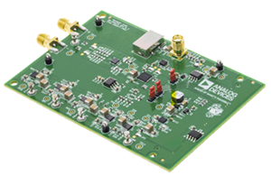
EVAL-AD5360EBZ
Analog Devices Inc.The AD5360 / AD5361?contain sixteen, 16-/14-bit DACs in a single 52-lead LQFP or 56-lead LFCSP package. They provide buffered voltage outputs with a span four times the reference voltage. The gain and offset of each DAC can be independently trimmed to remove errors. For even greater flexibility, the device is divided into two groups of eight DACs, and the output range of each group can be independently adjusted by an offset DAC.The AD5360 / AD5361 offer guaranteed operation over a wide supply range with VSS from ?4.5 V to ?16.5 V and VDD from +8 V to +16.5 V. The output amplifier headroom requirement is 1.4 V.The AD5360 / AD5361 have a high speed 4-wire serial interface, which is compatible with SPI, QSPI?, MICROWIRE?, and DSP interface standards and can handle clock speeds of up to 50 MHz. All the outputs can be updated simultaneously by taking the LDAC input low. Each channel has a programmable gain register and an offset adjust register.Each DAC output is amplified and buffered on-chip with respect to an external SIGGNDx input. The DAC outputs can also be switched to SIGGNDx via the CLR pin.APPLICATIONS Instrumentation Industrial control systems Level setting in automatic test equipment (ATE) Variable optical attenuators (VOA) Optical line cards
EVAL-AD5363EBZ
Analog Devices Inc.The AD5362?/ AD5363 contains 8, 16/14-bit DACs in a single, 56-lead, LFCSP or 52-lead LQFP package. It provides buffered voltage outputs with a span 4 times the reference voltage. The gain and offset of each DAC can be independently trimmed to remove errors. For even greater flexibility, the device is divided into two groups of 4 DACs, and the output range of each group can be independently adjusted by an offset DAC.The AD5362 / AD5363 offers guaranteed operation over a wide supply range with VSS from ?4.5 V to ?16.5 V and VDD from +8 V to +16.5 V. The output amplifier headroom requirement is 1.4 V operating with a load current of 1 mA.The AD5362 / AD5363 has a high-speed serial interface, which is compatible with SPI?, QSPI?, MICROWIRE?, and DSP interface standards and can handle clock speeds of up to 50 MHz. All the outputs can be updated simultaneously by taking the LDAC input low. Each channel has a programmable gain and an offset adjust register.Each DAC output is amplified and buffered on-chip with respect to an external SIGGND input. The DAC outputs can also be switched to SIGGND via the CLR pin.APPLICATIONS Instrumentation Industrial Control System Level setting in automatic test equipment (ATE) Variable optical attenuators (VOA) Optical line cards
EVAL-AD5370EBZ
Analog Devices Inc.The AD5370* contains forty 16-bit DACs in a single 64-lead LFCSP and a 64-lead LQFP. The device provides buffered voltage outputs with a span that is 4? the reference voltage. The gain and offset of each DAC channel can be independently trimmed to remove errors. For even greater flexibility, the device is divided into five groups of eight DACs. Three offset DAC channels allow the output range of blocks to be adjusted. Group 0 can be adjusted by Offset DAC 0, Group 1 can be adjusted by Offset DAC 1, and Group 2 to Group 4 can be adjusted by Offset DAC 2.The AD5370 offers guaranteed operation over a wide supply range, with VSS from ?16.5 V to ?4.5 V and VDD from +9 V to +16.5 V. The output amplifier headroom requirement is 1.4 V operating with a load current of 1 mA.The AD5370 has a high speed serial interface that is compatible with SPI, QSPI?, MICROWIRE?, and DSP interface standards and can handle clock speeds of up to 50 MHz.The DAC registers are updated on receipt of new data. All the outputs can be updated simultaneously by taking the LDAC input low. Each channel has a programmable gain and an offset adjust register to allow removal of gain and offset errors.Each DAC output is gained and buffered on chip with respect to an external SIGGNDx input. The DAC outputs can also be switched to SIGGNDx via the CLR pin.Applications Level setting in automatic test equipment (ATE) Variable optical attenuators (VOA) Optical switches Industrial control systems Instrumentation * Protected by U.S. Patent No. 5,969,657; other patents pending. ?
EVAL-AD5373EBZ
Analog Devices Inc.The AD5372?/ AD5373 contain 32, 16-bit or 14-bit digital-to-analog converters (DACs) in a single 64-lead LQFP. The devices provide buffered voltage outputs with a nominal span of 4? the reference voltage. The gain and offset of each DAC can be independently trimmed to remove errors. For even greater flexibility, the device is divided into four groups of eight DACs. Two offset DACs allow the output range of the groups to be altered. Group 0 can be adjusted by Offset DAC 0, and Group 1 to Group 3 can be adjusted by Offset DAC 1.The AD5372 / AD5373 offer guaranteed operation over a wide supply range: VSS from ?16.5 V to ?4.5 V and VDD from 9 V to 16.5 V. The output amplifier headroom requirement is 1.4 V operating with a load current of 1 mA.The ADAD5372 / AD5373 have a high-speed serial inter- face, which is compatible with SPI, QSPI?, MICROWIRE?, and DSP interface standards and can handle clock speeds of up to 50 MHz.The DAC registers are updated on reception of new data. All the outputs can be updated simultaneously by taking the LDAC input low. Each channel has a programmable gain and an offset adjust register.Each DAC output is gained and buffered on-chip with respect to an external SIGGNDx input. The DAC outputs can also be switched to SIGGNDx via the CLR pin.APPLICATIONS Level setting in automatic test equipment (ATE) Variable optical attenuators (VOA) Optical switches Industrial control systems Instrumentation
EVAL-AD5382SDZ
Analog Devices Inc.The AD5382 is a 32-channel, 14-Bit DAC and is available in a 14 mm?? 14 mm 100-lead LQFP package. It operates from a single 3 V or 5 V supply. Programmable gain (m) and offset (c) are provided per channel to facilitate system calibration. Each DAC channel is double-buffered which allows all DAC outputs to be updated simultaneously via an?LDAC pin. Each channel has an on-chip output amplifier which allows rail-to-rail operation. The AD5382 includes an internal 1.25 V/2.5 V low-drift reference. The AD5382 contains a parallel interface with a WR pulse width of 20 ns, a 30 MHz SPI interface and a 400 kHz I2C-compatible interface.This device is pin-to-pin compatible with the AD5380 (40-ch 14-bit DAC), the AD5381 (40-ch 12-bit DAC) and the AD5383 (32-ch 12-bit DAC).APPLICATIONS Variable optical attenuators (VOAs) Level setting (ATE) Optical micro-electro-mechanical systems (MEMS) Control systems Instrumentation
113758-HMC904LC5
Analog Devices Inc.The HMC904LC5 is a compact GaAs MMIC I/Q downconverter in a leadless RoHS compliant SMT package. This device provides a small signal conversion gain of 12 dB with a noise figure of 3 dB and 30 dB of image rejection across the frequency band. The HMC904LC5 utilizes an LNA followed by an image reject mixer which is driven by an active x2 multiplier.The image reject mixer eliminates the need for a filter following the LNA, and removes thermal noise at the image frequency. I and Q mixer outputs are provided and an external 90? hybrid is needed to select the required sideband. The HMC904LC5 is a much smaller alternative to hybrid style image reject mixer downconverter assemblies, and is compatible with surface mount manufacturing techniques.APPLICATIONS Point-to-Point and Point-to-Multi-Point Radio Military Radar, EW & ELINT Satellite Communications
115739-HMC573LC3B
Analog Devices Inc.The HMC573LC3B is a x2 active broadband frequency multiplier utilizing GaAs PHEMT technology in a leadless RoHS compliant SMT package. When driven by a +5 dBm signal, the multiplier provides +12 dBm typical output power from 8 to 22 GHz. The Fo and 3Fo isolations are >20 dBc and >25 dBc respectively at 16 GHz.The HMC573LC3B is ideal for use in LO multiplier chains for Pt to Pt & VSAT Radios yielding reduced parts count vs. traditional approaches. The low additive SSB Phase Noise of -134 dBc/Hz at 100 kHz offset helps maintain good system noise performance. The RoHS packaged HMC573LC3B eliminates the need for wire bonding, and allows the use of surface mount manufacturing techniques.APPLICATIONS Clock Generation Applications: SONET OC-192 & SDH STM-64 Point-to-Point & VSAT Radios Test Instrumentation Military & Space
116108-HMC699LP5
Analog Devices Inc.The HMC699LP5(E) is a frequency synthesizer with a wideband reversible polarity digital PFD and lock detect output. The divider operates from 160 - 7000 MHz with a continuous integer division ratio N = 56 to 519 and non-continuous division ratio N = 16 to 54. The HMC699LP5(E) high frequency operation along with ultra low phase noise floor make possible synthesizers with wide loop bandwidth and low N resulting in fast settling and very low phase noise. When used in conjunction with a differential loop filter, the HMC699LP5(E) can be used to phase lock a VCO to a reference oscillator. For continuous division ratio, the A counter and S counter must satisfy the condition: A + 1 ?? S.APPLICATIONS Satellite Communication Systems Point-to-Point Radios Military Applications Sonet Clock Generation
116960-HMC625BLP5
Analog Devices Inc.The HMC625BLP5E is a digitally controlled variablegain amplifier which operates from DC to 5 GHz, andcan be programmed to provide anywhere from 13.5dB attenuation, to 18 dB of gain, in 0.5 dB steps. TheHMC625BLP5E delivers noise figure of 6 dB in itsmaximum gain state, with output IP3 of up to +32 dBmin any state. The dual mode control interface is CMOS/TTL compatible, and accepts either a three wire serialinput or a 6 bit parallel word. The HMC625BLP5E alsofeatures a user selectable power up state and a serialoutput port for cascading other Hittite serial controlledcomponents. The HMC625BLP5E is housed in aRoHS compliant 5x5 mm QFN leadless package, andrequires no external matching components.Applications Cellular/3G infrastructure WiBro / WiMAX / 4G Microwave radio & VSAT Test equipment and sensors IF & RF applications
116993-HMC705LP4
Analog Devices Inc.The HMC705LP4(E) is a low noise GaAs HBT programmable divider in a 4x4 mm leadless surface mount package. The divider can be programmed to divide by any number from N = 1 to N = 17 up to 6.5 GHz. The HMC705LP4E's high frequency operation along with low phase noise floor is very useful in high performance fast settling synthesizer architectures. The HMC705LP4E may be combined with Hittite's Phase Frequency Detectors, VCOs and PLL ICs to create low noise, fast settling phase locked loops.APPLICATIONS Satellite Communication Systems Point-to-Point Radios Military Applications Sonet Clock Generation Test Equipment
119681-HMC677LP5
Analog Devices Inc.The HMC677 devices are multifunction BiCMOS control interface integrated circuits (ICs), which are ideal for driving the gates of field effect transistor (FET) and pseudomorphic high electron mobility transistor (pHEMT) based monolithic microwave integrated circuit (MMIC) control devices. This unique IC can be used to simplify the control of microwave and millimeterwave transmit/receive modules, military subsystems, and multithrow/multiport test and measurement equipment. The HMC677 devices accept serial or parallel data and can drive up to six complementary sets of outputs.The HMC677 devices also provide additional functionality such as a power-up state selection, adjustable output voltage levels, and a latched parallel control mode which allows multiple control devices to share a common data bus. The HMC677 devices are ideal for controlling digital phase shifters, digital attenuators, digital variable gain amplifiers, and switching matrices embedded in complex microwave and millimeterwave assemblies.APPLICATIONS Microwave and millimeterwave control circuits Test and measurement equipment Complex multifunction assemblies Military and space subsystems Transmit/receive module controllers
119916-HMC689LP4
Analog Devices Inc.The HMC689LP4(E) is a high dynamic range passive MMIC mixer with integrated LO amplifier in a 4x4 SMT QFN package covering 2.0 - 2.7 GHz. Excellent input IP3 performance of +32 dBm for down conversion is provided for 3G & 4G GSM/CDMA applications at an LO drive of 0 dBm. With an input 1 dB compression of +23 dBm, the RF port will accept a wide range of input signal levels. Conversion loss is 7.5 dB typical. The DC to 800 MHz IF frequency response will satisfy GSM/CDMA transmit or receive frequency plans. The HMC689LP4(E) is pin for pin compatible with the?HMC688LP4(E)?which is a 2.0 - 2.7 MHz mixer with LO amplifier, amplifier is optimized for low side LO applications.APPLICATIONS Cellular/3G & LTE/WiMAX/4G Basestations & Repeaters GSM, CDMA & OFDM Transmitters and Receivers
122517-HMC744LC3
Analog Devices Inc.The HMC744LC3?is a 1:2 Fanout Buffer designed to support data transmission rates up to 14 Gbps, and clock frequencies as high as 14 GHz.All differential inputs to the HMC744LC3 are CML and terminated on-chip with 50 Ohms to the positive supply, Vcc, and may be AC or DC coupled. The differential CML outputs are source terminated to 50 Ohms and may also be AC or DC coupled. Outputs can be connected directly to a 50 Ohm Vcc-terminated system, while DC blocking capacitors may be used if the terminating system is 50 Ohms to ground. The HMC744LC3 also features an output level control pin, VR, which allows for loss compensation or signal-level optimization. the HMC744LC3 operates from a single 3.3 V supply and is available in ROHS-compliant 3?3 mm SMT package.APPLICATIONS RF ATE Applications Broadband Test & Measurement Serial Data Transmission up to 14 Gbps Clock Buffering up to 14 GHz
122517-HMC746LC3C
Analog Devices Inc.The HMC746LC3C is an AND/NAND/OR/NOR function designed to support data transmission rates of up to 14 Gbps, and clock frequencies as high as 14 GHz. The HMC746LC3C may be easily configured to provide any of the following logic functions: AND, NAND, OR and NOR.All differential inputs to the HMC746LC3C are CML and terminated on-chip with 50 Ohms to the positive supply, Vcc, and may be AC or DC coupled. The differential CML outputs are source terminated to 50 Ohms and may also be AC or DC coupled. Outputs can be connected directly to a 50 Ohm Vcc-terminated system, while DC blocking capacitors may be used if the terminating system is 50 Ohms to ground. The HMC746LC3C also features an output level control pin, VR, which allows for loss compensation or signal-level optimization. the HMC746LC3C operates from a single 3.3 V supply and is available in ROHS-compliant 3x3 mm SMT package.APPLICATIONS RF ATE Applications Broadband Test & Measurement Serial Data Transmission up to 13 Gbps Digital Logic Systems up to 13 GHz NRZ-to-RZ Conversion
123576-HMC729LC3C
Analog Devices Inc.The HMC729LC3C is a T Flip-Flop w/Reset designed to support clock frequencies as high as 26 GHz. During normal operation, with the reset pin not asserted, the output toggles from its prior state on the positive edge of the clock. This results in a divide-by-two function of the clock input. Asserting the reset pin forces the Q output low regardless of the clock edge state (asynchronous reset assertion). Reversing the clock inputs allows for negative-edge triggered applications.All input signals to the HMC729LC3C are terminated with 50 to ground on-chip, and may be either AC or DC coupled. Outputs can be connected directly to a 50 terminated system, while DC blocking capacitors may be used if the terminating system is 50 to a non-ground DC voltage. The HMC729LC3C operates from a single -3.3V DC supply and is available in a ceramic RoHS compliant 3x3 mm SMT package.APPLICATIONS Serial Data Transmission up to 26 Gbps High Speed Frequency Divider (up to 26 GHz) Broadband Test & Measurement RF ATE Applications
123815-HMC751LC4
Analog Devices Inc.The HMC751 is a high dynamic range GaAs PHEMT MMIC Low Noise Amplifier (LNA) housed in a leadless 'Pb free' RoHS compliant SMT package. The HMC751 provides 25 dB of small signal gain, 2.2 dB of noise figure and output IP3 of +25 dBm. The P1dB output power of +13 dBm also enables the LNA to function as a LO driver for balanced, I/Q or image reject mixers. The HMC751 allows the use of surface mount manufacturing techniques.Applications Point-to-Point Radios Point-to-Multi-Point Radios & VSAT Test Equipment and Sensors Military
124352-HMC860LP3E
Analog Devices Inc.The HMC860LP3E is a BiCMOS ultra low noise quad-output voltage regulator. It features a low noise band-gap reference externally decoupled for best in-close noise performance. High Power Supply Rejection Ratio (PSRR) in the 0.1 MHz to 10 MHz range provides excellent rejection of preceding switching regulator noise. The four voltage outputs are ideal for frequency generation subsystems including Hittite's broad line of PLLs with Integrated VCOs. Each output voltage can be adjusted higher or lower than the default value by using one external resistor.Each output can be set to 5V by grounding the corresponding HV pin. The regulator can be powered down by the TTL-compatible Enable input. The HMC860LP3E is housed in a 3 ? 3mm QFN SMT package.APPLICATIONS Test Instrumentation Military Radios, Radar and ECM Basestation Infrastructure Ultra Low Noise Frequency Generation Fractional-N Synthesizer Supply Mixed-Signal Circuit Supply
125228-HMC759LP3E
Analog Devices Inc.The HMC759LP3E is a 7-bit BiCMOS Digital Attenuator in a low cost leadless SMT package. This versatile digital attenuator incorporates off-chip AC ground capacitors for near DC operation, making it suitable for a wide variety of RF and IF applications. The control interface is CMOS/TTL compatible and accepts a three wire serial input. The HMC759LP3E features user selectable power up states and a serial output port for cascading other Hittite serial controlled components. The HMC759LP3E is housed in a RoHS compliant 3?3 mm QFN leadless package, and occupies only 9 mm2.APPLICATIONS Cellular/3G Infrastructure WiBro/WiMAX/4G Microwave Radio & VSAT Test Equipment and Sensors IF & RF Applications
125354-HMC785LP4E
Analog Devices Inc.The HMC785LP4E is a high dynamic range passive MMIC mixer with integrated LO amplifier in a 4x4 SMT QFN package covering 1.7 to 2.2 GHz. Excellent input IP3 performance of +38 dBm for down conversion is provided for 3G & 4G GSM/CDMA applications at an LO drive of 0 dBm. With an input 1 dB compression of +26 dBm, the RF port will accept a wide range of input signal levels. Conversion loss is 8 dB typical. Up to 300 MHz IF frequency response will satisfy GSM/CDMA transmit or receive frequency plans. The HMC785LP4E is optimized for low side LO frequency plans for 1.7 - 2.2 GHz RF Band and is pin for pin compatible with the HMC685LP4E.APPLICATIONS Cellular/3G & LTE/WiMAX/4G Basestations & Repeaters GSM, CDMA & OFDM Transmitters and Receivers
126223-HMC789ST89E
Analog Devices Inc.The HMC789ST89E is a high linearity GaAs InGaP HBT gain block MMIC operating from 0.7 to 2.8 GHz and packaged in an industry standard SOT89 package. Utilizing a minimum number of external components and a single +5V supply, the amplifier output IP3 can be optimized to +45 dBm. The high output IP3 and high gain make the HMC789ST89E ideal for use in PA driver & pre-driver applications in Cellular/4G and Fixed Wireless.Applications Cellular/4G Fixed Wireless & WLAN CATV, Cable Modem & DBS Microwave Radio & Test Equipment IF & RF Applications


