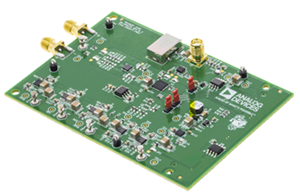
AD9522-4/PCBZ
Analog Devices Inc.The AD9522-41 provides a multioutput clock distributionfunction with subpicosecond jitter performance, along with an on-chip PLL and VCO. The on-chip VCO tunes from 1.4 GHz to 1.8 GHz. An external 3.3 V/5 V VCO/VCXO of up to 2.4 GHz can also be used.The AD9522 serial interface supports both SPI and I2C? ports. An in-package EEPROM can be programmed through the serial interface and store user-defined register settings for power-up and chip reset.The AD9522 features 12 LVDS outputs in four groups. Any of the 800 MHz LVDS outputs can be reconfigured as two 250 MHz CMOS outputs.Each group of outputs has a divider that allows both the divideratio (from 1 to 32) and the phase (coarse delay) to be set.The AD9522 is available in a 64-lead LFCSP and can be operatedfrom a single 3.3 V supply. The external VCO can have an operating voltage up to 5.5 V.The AD9522 is specified for operation over the standard industrialrange of ?40?C to +85?C.The AD9520-4 is an equivalent part to the AD9522-4 featuringLVPECL / CMOS drivers instead of LVDS / CMOS drivers.1The AD9522 is used throughout this data sheet to refer to all the members of the AD9522 family. However, when AD9522-4 is used, it is referring to that specificmember of the AD9522 family.ApplicationsLow jitter, low phase noise clock distributionClock generation and translation for SONET, 10Ge, 10G FC, and other 10 Gbps protocolsForward error correction (G.710)Clocking high speed ADCs, DACs, DDSs, DDCs, DUCs, MxFEsHigh performance wireless transceiversATE and high performance instrumentationBroadband infrastructuresData Sheet, Rev. 0, 10/08
AD9522-5/PCBZ
Analog Devices Inc.The AD9522-51 provides a multioutput clock distribution function with subpicosecond jitter performance, along with an on-chip PLL that can be used with an external VCO.???The AD9522 serial interface supports both SPI and I2C? ports. An in-package EEPROM can be programmed through the serial interface and store user-defined register settings for power-up and chip reset.The AD9522 features 12 LVDS outputs in four groups. Any of the 800 MHz LVDS outputs can be reconfigured as two 250 MHz CMOS outputs.Each group of outputs has a divider that allows both the divide ratio (from 1 to 32) and the phase (coarse delay) to be set.The AD9522 is available in a 64-lead LFCSP and can be operated from a single 3.3 V supply. The external VCO can have an operating voltage up to 5.5 V.The AD9522 is specified for operation over the standard industrial range of ?40?C to +85?C.The AD9520-5 is an equivalent part to the AD9522-5 featuring LVPECL/CMOS drivers instead of LVDS/CMOS drivers.1The AD9522 is used throughout this data sheet to refer to all the members of the AD9522 family. However, when AD9522-5 is used, it is referring to that specific member of the AD9522 family.ApplicationsLow jitter, low phase noise clock distributionClock generation and translation for SONET, 10Ge, 10G FC, and other 10 Gbps protocolsForward error correction (G.710)Clocking high speed ADCs, DACs, DDSs, DDCs, DUCs, MxFEsHigh performance wireless transceiversATE and high performance instrumentationBroadband infrastructures
AD9524/PCBZ
Analog Devices Inc.The AD9524 provides a low power, multi-output, clock distribution function with low jitter performance, along with an on-chip PLL and VCO. The on-chip VCO tunes from 3.6 GHz to 4.0 GHz.The AD9524 is designed to support the clock requirements for long term evolution (LTE) and multicarrier GSM base station designs. It relies on an external VCXO to provide the reference jitter cleanup to achieve the restrictive low phase noise requirements necessary for acceptable data converter SNR performance.The input receivers, oscillator, and zero delay receiver provide both single-ended and differential operation. When connected to a recovered system reference clock and a VCXO, the device generates six low noise outputs with a range of 1 MHz to 1 GHz, and one dedicated buffered output from the input PLL (PLL1). The frequency and phase of one clock output relative to another clock output can be varied by means of a divider phase select function that serves as a jitter-free coarse timing adjustment in increments that are equal to one-half the period of the signal coming out of the VCO.An in-package EEPROM can be programmed through the serial interface to store user-defined register settings for power-up and chip reset.APPLICATIONS LTE and multicarrier GSM base stations Wireless and broadband infrastructure Medical instrumentation Clocking high speed ADCs, DACs, DDSs, DDCs, DUCs, MxFEs Low jitter, low phase noise clock distribution Clock generation and translation for SONET, 10Ge, 10G FC, and other 10 Gbps protocols Forward error correction (G.710) High performance wireless transceivers ATE and high performance instrumentation
AD9525/PCBZ
Analog Devices Inc.The AD9525 is designed to support converter clock requirements for long-term evolution (LTE) and multicarrier GSM base station designs.The AD9525 provides a low power, multioutput, clock distribution function with low jitter performance, along with an on-chip PLL that can be used with an external VCO or VCXO. The VCO input and eight LVPECL outputs can operate up to a frequency of 3.6 GHz. All outputs share a common divider that can provide a division of 1 to 6.The AD9525 offers a dedicated output that can be used to provide a programmable signal for resetting or synchronizing a data converter. The output signal is activated by a SPI write.The AD9525 is available in a 48-lead LFCSP and can be operated from a single 3.3 V supply. The external VCXO or VCO can have an operating voltage of up to 5.5 V.The AD9525 operates over the extended industrial temperature range of ?40?C to +85?C.Applications LTE and multicarrier GSM base stations Clocking high speed ADCs, DACs ATE and high performance instrumentation 40/100Gb/s OTN Line Side Clocking Cable/DOCSIS CMTS Clocking Test and Measurement
AD9531/PCBZ
Analog Devices Inc.The AD9531 provides a multioutput clock generator function and three on-chip phase-locked loop (PLL) cores with SPI programmable output frequencies and formats.PLL1 provides two reference inputs and 10 outputs and includes four user selectable loop configurations. The PLL has a fully integrated loop filter requiring only a single external capacitor (or a series RC network). PLL1 provides a wide range of output frequencies up to 400 MHz and is capable of operating with an external voltage controlled crystal oscillator (VCXO) and loop filter, instead of the integrated voltage controlled oscillator (VCO) and loop filter.PLL2 is an integer-N PLL providing a single reference input and 12 outputs. PLL2 synthesizes output frequencies up to 400 MHz from the REF2_x source and synchronizes the output clocks to the input reference.PLL3 provides a single reference input and two outputs. PLL3 synthesizes output frequencies up to 400 MHz from the REF3_x source and synchronizes the output clocks to input reference.The AD9531 is available in an 88-lead LFCSP and is specified over the ?40?C to +85?C operating temperature range.Throughout this data sheet, multifunction pins, such as LOR/M4, are referred to either by the entire pin name or by a single function of the pin (for example, LOR, when only that function is relevant). In other cases, the text and figures of this data sheet contain references to a channel rather than a pin. For example, REF_A refers to the REF_A channel rather than the REF_AP and REF_AN pins. Likewise, OUT3_1 refers to Channel 1 of PLL3 rather than the OUT3_1P and OUT3_1N pins. Additionally, an abbreviated notation for a pin pair replaces an explicit reference to a each pin (for example, REF_Ax signifies the REF_AN and REF_AP pins.).Applications Radio equipment controller clocking Low jitter/phase noise clock generation and distribution Clock generation and translation for SONET, 10GE, 10G FC, and other 10 Gbps protocols 40 Gbps/100 Gbps networking line cards, including SONET, synchronous ethernet, OTU2/3/4 Forward error correction (G.710) High performance wireless transceivers ATE and high performance instrumentation Broadband infrastructures Ethernet line cards, switches, and routers SATA and PCI-express
AD9545/PCBZ
Analog Devices Inc.The AD9545 supports existing and emerging International Telecommunications Union (ITU) standards for the delivery of frequency, phase, and time of day over service provider packet networks, including ITU-G.8262, ITU-T G.812, ITU-T G.813, ITU-T G.823, ITU-T G.824, ITU-T G.825, and ITU-T G.8273.2.The 10 clock outputs of the AD9545 are synchronized to any one of up to four input references. The digital phase-locked loops (DPLLs) reduce timing jitter associated with the external references. The digitally controlled loop and holdover circuitry continuously generate a low jitter output signal, even when all reference inputs fail.The AD9545 is available in a 48-lead LFCSP (7 mm ? 7 mm) package and operates over the ?40?C to +85?C temperature range.Note that throughout the data sheet, multifunction pins, such as SDO/M5, are referred to either by the entire pin name or by a single function of the pin, for example, M5, when only that function is relevant.APPLICATIONS Global positioning system (GPS), PTP (IEEE 1588), and synchronous Ethernet (SyncE) jitter cleanup and synchronization Optical transport networks (OTN), synchronous digital hierarchy (SDH), and macro and small cell base stations Small base station clocking, including baseband and radio Stratum 2, Stratum 3e, and Stratum 3 holdover, jitter cleanup, and phase transient control JESD204B support for analog-to-digital converter (ADC) and digital-to-analog converter (DAC) clocking Cable infrastructures Carrier Ethernet
AD9548/PCBZ
Analog Devices Inc.The AD9548 provides synchronization for many systems, including synchronous optical networks (SONET/SDH). The AD9548 generates an output clock synchronized to one of up to four differential or eight single-ended external input references. The digital PLL allows for reduction of input time jitter or phase noise associated with the external references. The AD9548 continuously generates a clean (low jitter), valid output clockeven when all references have failed by means of a digitallycontrolled loop and holdover circuitry.The AD9548 operates over an industrial temperature range of?40?C to +85?C.ApplicationsNetwork synchronizationCleanup of reference clock jitterGPS 1 pulse per second synchronizationSONET/SDH clocks up to OC-192, including FECStratum 2 holdover, jitter cleanup, and phase transient controlStratum 3E and Stratum 3 reference clocksWireless base stations, controllersCable infrastructureData communications
AD9558/PCBZ
Analog Devices Inc.The AD9558 is a low loop bandwidth clock multiplier that providesjitter cleanup and synchronization for many systems, includingsynchronous optical networks (OTN/SONET/SDH). The AD9558generates an output clock synchronized to up to four external inputreferences. The digital phase-locked loop (PLL) allows reductionof input time jitter or phase noise associated with the externalreferences. The digitally controlled loop and holdover circuitryof the AD9558 continuously generates a low jitter output clockeven when all reference inputs have failed.The AD9558 operates over an industrial temperature range of?40?C to +85?C. If a smaller package is required, refer to theAD9557 for the two-input/two-output version of the same device.Applications Network synchronization, including synchronous Ethernet and SDH to OTN mapping/demapping Cleanup of reference clock jitter SONET/SDH/OTN clocks up to 100 Gbps, including FEC Stratum 3 holdover, jitter cleanup, and phase transient control Wireless base station controllers Cable infrastructure Data communications
AD9571-EVALZ-LVD
Analog Devices Inc.The AD9571 provides a multioutput clock generator function comprising a dedicated PLL core that is optimized for Ethernet line card applications. The integer-N PLL design is based on the Analog Devices, Inc., proven portfolio of high performance, low jitter frequency synthesizers to maximize network performance. Other applications with demanding phase noise and jitter requirements also benefit from this part.The PLL section consists of a low noise phase frequency detector (PFD), a precision charge pump (CP), a low phase noise voltage controlled oscillator (VCO), and a preprogrammed feedback divider and output divider. By connecting an external crystal or reference clock to the REFCLK pin, frequencies up to 156.25 MHz can be locked to the input reference.Each output divider and feedback divider ratio is preprogrammed for the required output rates. No external loop filter components are required, thus conserving valuable design time and board space.The AD9571 is available in a 40-lead 6 mm ? 6 mm lead frame chip scale package and can be operated from a single 3.3 V supply. The operating temperature range is ?40?C to +85?C.APPLICATIONS Ethernet line cards, switches, and routers SCSI, SATA, and PCI-express PCI support included Low jitter, low phase noise clock generation
AD9608-125EBZ
Analog Devices Inc.The AD9608 is a monolithic, dual-channel, 1.8 V supply, 10-bit, 105 MSPS/125 MSPS analog-to-digital converter (ADC) that features a high performance sample-and-hold circuit and an on-chip voltage reference.The product uses multistage differential pipeline architecture with output error correction logic to provide 10-bit accuracy at 125 MSPS data rates and to guarantee no missing codes over the full operating temperature range.The ADC contains several features designed to maximize flexibility and minimize system cost, such as programmable clock and data alignment and programmable digital test pattern generation. The available digital test patterns include built-in deterministic and pseudorandom patterns, along with custom user-defined test patterns entered via the serial port interface (SPI).A differential clock input controls all internal conversion cycles. An optional duty cycle stabilizer (DCS) compensates for wide variations in the clock duty cycle while maintaining excellent overall ADC performance.The digital output data is presented in offset binary, Gray code, or twos complement format. A data output clock (DCO) is provided for each ADC channel to ensure proper latch timing with receiving logic. Logic levels of 1.8 V CMOS and 1.8 V LVDS are supported. Output data can also be multiplexed onto a single output bus.The AD9608 is available in a 64-lead RoHS-compliant LFCSP and is specified over the industrial temperature range (?40?C to +85?C).PRODUCT HIGHLIGHTS Operates from a single 1.8 V analog power supply and features a separate digital output driver supply to accommodate 1.8 V CMOS or 1.8 V LVDS logic families. The patented sample-and-hold circuit maintains excellent performance for input frequencies up to 200 MHz and is designed for low cost, low power, and ease of use. Includes a standard serial port interface that supports various product features and functions, such as data output format-ting, internal clock divider, power-down, DCO/data timing, and offset adjustments. Packaged in a 64-lead, RoHS-compliant LFCSP that is pin compatible with the AD9650, AD9269 and AD9268 16-bit ADC?s, the AD9258 and AD9648 14-bit ADC, the AD9628 and AD9231 12-bit ADC?s, and the AD9204 10-bit ADC?s, enabling a simple migration path between 10-bit and 16-bit converters sampling from 20 MSPS to 125 MSPS.APPLICATIONS Communications Diversity radio systems I/Q demodulation systems Broadband data applications Battery-powered instruments Hand held scope meters Portable medical imaging Ultrasound
AD9613-250EBZ
Analog Devices Inc.The AD9613 is a dual 12-bit, analog-to-digital converter (ADC) with sampling speeds up to 250 MSPS. The AD9613 is designed to support communications applications where low cost, small size, wide bandwidth and versatility are desired.The dual ADC core features a multistage, differential pipelinedarchitecture with integrated output error correction logic. EachADC features wide bandwidth inputs supporting a variety of user-selectable input ranges. An integrated voltage reference eases design considerations. A duty cycle stabilizer is provided to compensate for variations in the ADC clock duty cycle, allowing the converters to maintain excellent performance.The ADC output data are routed directly to the two external 12-bit LVDS output ports and formatted either as interleaved or channel multiplexed.Flexible power-down options allow significant power savings,when desired.Programming for setup and control are accomplished using a 3-wire SPI-compatible serial interface.The AD9613 is available in a 64-lead LFCSP and is specified overthe industrial temperature range of ?40?C to +85?C.PRODUCT HIGHLIGHTS Integrated dual, 12-bit, 170 MSPS/210 MSPS/250 MSPS ADCs. Fast overrange and threshold detect. Proprietary differential input maintains excellent SNR performance for input frequencies up to 400 MHz. SYNC input allows synchronization of multiple devices. 3-pin, 1.8V SPI port for register programming and register readback. Pin compatibility with the AD9643, allowing a simple migration up to 14 bits, and with the AD6649 and the AD6643.APPLICATIONS Communications Diversity radio systems Multimode digital receivers (3G) TD-SCDMA, WiMax, WCDMA, CDMA2000, GSM, EDGE, LTE I/Q demodulation systems Smart antenna systems General-purpose software radios Ultrasound equipment Broadband data applications
104711-HMC401QS16G
Analog Devices Inc.The HMC401QS16G(E) is a GaAs InGaP Heterojunction Bipolar Transistor (HBT) MMIC VCO. The HMC401QS16G(E)?? ?integrates a resonator, negative resistance device, varactor diode and a divide-by-8 prescaler. The VCO?s phase noise performance is excellent over temperature, shock, and process due to the oscillator?s monolithic structure. Power output is -7 dBm typical from a 5V supply voltage. The voltage controlled oscillator is packaged in a low cost, surface mount 16 leaded QSOP package with an exposed base for improved RF and thermal performance.Applications Point-to-Point Radios Point-to-Multi-Point Radios / LMDS VSAT
104713-HMC358MS8G
Analog Devices Inc.The HMC358MS8G(E) is a GaAs InGaP Heterojunction Bipolar Transistor (HBT) MMIC VCO. The HMC358MS8G(E) integrates resonators, negative resistance devices, varactor diodes, and buffer amplifiers. The VCO?s phase noise performance is excellent over temperature, shock, and process due to the oscillator?s monolithic structure. Power output is 11 dBm typical from a 3V supply voltage. The voltage controlled oscillator is packaged in a low cost, surface mount 8 lead MSOP package with an exposed base for improved RF and thermal performance.APPLICATIONS UNII & Point-to-Point Radios 802.11a & HiperLAN WLAN VSAT Radios
105180-HMC408LP3
Analog Devices Inc.The HMC408LP3(E) is a 5.1 - 5.9 GHz high efficiency GaAs InGaP Heterojunction Bipolar Transistor (HBT) Power Amplifier MMIC which offers +30 dBm P1dB. The amplifier provides 20 dB of gain, +32.5 dBm of saturated power, and 27% PAE from a +5V supply voltage. The input is internally matched to 50 Ohms while the output requires a minimum of external components. Vpd can be used for full power down or RF output power/current control. The amplifier is packaged in a low cost, 3x3 mm leadless surface mount package with an exposed base for improved RF and thermal performance.Applications 802.11a & HiperLAN WLAN UNII & Pt-to-Pt / Multi-Point Radios Access Point Radios
105706-HMC416LP4
Analog Devices Inc.The HMC416LP4(E) is a GaAs InGaP Heterojunction Bipolar Transistor (HBT) MMIC VCO with integrated resonator, negative resistance device, varactor diode, and buffer amplifier. Covering 2.75 to 3.0 GHz, the VCO?s phase noise performance is excellent over temperature, shock, vibration and process due to the oscillator?s monolithic structure. Power output is 4.5 dBm typical from a single supply of 3V @ 37 mA. The voltage controlled oscillator is packaged in a low cost leadless QFN 4?4 mm surface mount package.APPLICATIONS Wireless Infrastructure Industrial Controls Test Equipment Military
105706-HMC430LP4
Analog Devices Inc.The HMC430LP4(E) is a GaAs InGaP Heterojunction Bipolar Transistor (HBT) MMIC VCO with an integrated resonator, negative resistance device, varactor diode, and buffer amplifier. The VCO?s phase noise performance is excellent over temperature, shock, vibration and process due to the oscillator?s monolithic structure. Power output is 2 dBm typical from a 3V supply voltage. The voltage controlled oscillator is packaged in a low cost leadless QFN 4x4 mm surface mount package.APPLICATIONS 802.11a & HiperLAN WLAN? VSAT Radios? UNII & Point-to-Point Radios
106058-HMC455LP3
Analog Devices Inc.The HMC455LP3(E) is a high output IP3 GaAs InGaP Heterojunction Bipolar Transistor (HBT) 1?2 watt MMIC amplifier operating between 1.7 and 2.5 GHz. Utilizing a minimum number of external components the amplifier provides 13 dB of gain and +28 dBm of saturated power at 56% PAE from a single +5 Vdc supply voltage. The high output IP3 of +42 dBm coupled with the low VSWR of 1.4:1 make the HMC455LP3(E) ideal driver amplifier for PCS/3G wireless infrastructures. A low cost, leadless 3x3 mm QFN surface mount package (LP3) houses the linear amplifier. The LP3 provides an exposed base for excellent RF and thermal performance.Applications Multi-Carrier Systems? GSM, GPRS & EDGE? CDMA & WCDMA? PHS
106137-HMC695LP4
Analog Devices Inc.The HMC695LP4(E) are active miniature x4 frequency multipliers utilizing InGaP GaAs HBT technology in 4x4 mm leadless surface mount packages. Power output is +7 dBm typical from a +5V supply voltage and varies little vs. input power, temperature and supply voltage. Suppression of undesired fundamental and sub-harmonics is >25 dBc typical with respect to output signal level. The low additive SSB phase noise of -140 dBc/Hz at 100 kHz offset helps the user maintain good system noise performance. The HMC695LP4(E) are ideal for use in LO multiplier chains allowing reduced parts count vs. traditional approaches.APPLICATIONS Fiber Optic Applications Point-to-Point Radios Military Radar
106651-HMC533LP4
Analog Devices Inc.The HMC533LP4(E) are GaAs InGaP Heterojunction Bipolar Transistor (HBT) MMIC VCOs. The HMC533LP4(E) integrate resonators, negative resistance devices, varactor diodes and feature a divide-by-16 output. T he VCO?s phase noise performance is excellent over temperature, shock, and process due to the oscillator?s monolithic structure. Power output is +12 dBm typical from a +5V supply voltage. Prescaler function can be disabled to conserve current if not required. The voltage controlled oscillator is packaged in a leadless QFN 4x4 mm surface mount package.APPLICATIONS VSAT Radio Point-to-Point/Multi-point Radio Test Equipment & Industrial Controls Military End-Use Automotive Radar
107220-HMC373LP3
Analog Devices Inc.The HMC373LP3 / HMC373LP3E are versatile, high?dynamic range GaAs MMIC Low Noise Amplifiers?that integrates a low loss LNA bypass mode on the?IC. The amplifier is ideal for GSM & CDMA cellular?basestation front-end receivers operating between?700 and 1000 MHz and provides 0.9 dB noise figure,?14 dB of gain and +35 dBm IP3 from a single supply of?+5V @ 90 mA. Input and output return losses are 28?and 12 dB respectively with the LNA requiring minimal?external components to optimize the RF input match,?RF ground and DC bias. By presenting an open or?short circuit to a single control line, the LNA can be?switched into a low 2.0 dB loss bypass mode reducing?the current consumption to 10 ?A. For applications?which require improved noise figure, please see the?HMC668LP3(E).Applications GSM, GPRS & EDGE CDMA & W-CDMA Private Land Mobile Radio


