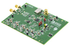
DC082B
Analog Devices Inc.The LT1182/LT1183 are dual current mode switching regulators that provide the control function for Cold Cathode Fluorescent Lighting (CCFL) and Liquid Crystal Display (LCD) Contrast. The LT1184/LT1184F provide only the CCFL function. The ICs include high current, high efficiency switches, an oscillator, a reference, output drive logic, control blocks and protection circuitry. The LT1182 permits positive or negative voltage LCD contrast operation. The LT1183 permits unipolar contrast operation and pins out an internal reference. The LT1182/LT1183 support grounded and floating lamp configurations. The LT1184F supports grounded and floating lamp configurations. The LT1184 supports only grounded lamp configurations.Applications Notebook and Palmtop Computers Portable Instruments Automotive Displays Retail Terminals
DC093A
Analog Devices Inc.The LT1371 is a monolithic high frequency current mode switching regulator. It can be operated in all standard switching configurations including boost, buck, flyback, forward, inverting and ?Cuk?. A 3A high efficiency switch is included on the die, along with all oscillator, control and protection circuitry.The LT1371 typically consumes only 4mA quiescent current and has higher efficiency than previous parts. High frequency switching allows for very small inductors to be used.New design techniques increase flexibility and maintain ease of use. Switching is easily synchronized to an external logic level source. A logic low on the Shutdown pin reduces supply current to 12?A. Unique error amplifier circuitry can regulate positive or negative output voltage while maintaining simple frequency compensation techniques. Nonlinear error amplifier transconductance reduces output overshoot on start-up or overload recovery. Oscillator frequency shifting protects external components during overload conditions.Applications Boost Regulators Laptop Computer Supplies Multiple Output Flyback Supplies Inverting Supplies
DC1009A-A
Analog Devices Inc.The LTC2492 is a 4-channel (2-channel differential), 24-bit, No Latency ??? ADC with Easy Drive technology. The patented sampling scheme eliminates dynamic input current errors and the shortcomings of on-chip buffering through automatic cancellation of differential input current. This allows large external source impedances and rail-to-rail input signals to be directly digitized while maintaining exceptional DC accuracy. The LTC2492 includes a high accuracy temperature sensor and an integrated oscillator. This device can be configured to measure an external signal (from combinations of 4 analog input channels operating in single-ended or differential modes) or its internal temperature sensor. It can be programmed to reject line frequencies of 50Hz, 60Hz, or simultaneous 50Hz/60Hz and configured to double its output rate. The integrated temperature sensor offers 1/30th?C resolution and 2?C absolute accuracy. The LTC2492 allows a wide common mode input range (0V to VCC), independent of the reference voltage. Any combination of single-ended or differential inputs can be selected and the first conversion after a new channel selection is valid.Applications Direct Sensor Digitizer Direct Temperature Measurement Instrumentation Industrial Process Control
LTC2487 | 16-bit 4/2-channel I2C Easy Drive ADC (Requires DC590B)
Analog Devices Inc.DC1010A-C: Demo Board for the LTC2487 16-Bit 2-/4-Channel ΔΣ ADC with PGA, Easy Drive and I2C Interface.
DC1011A-A
Analog Devices Inc.The LTC2498 is a 16-channel (8-differential) 24-bit No Latency ??? ADC with Easy Drive technology. The patented sampling scheme eliminates dynamic input current errors and the shortcomings of on-chip buffering through automatic cancellation of differential input current. This allows large external source impedances, and rail-to-rail input signals to be directly digitized while maintaining exceptional DC accuracy. The LTC2498 includes a high accuracy temperature sensor and an integrated oscillator. This device can be configured to measure an external signal (from combinations of 16 analog input channels operating in single ended or differential modes) or its internal temperature sensor. The integrated temperature sensor offers 1/30th ?C resolution and 2?C absolute accuracy. The LTC2498 allows a wide common mode input range (0V to VCC), independent of the reference voltage. Any combination of single-ended or differential inputs can be selected and the first conversion after a new channel is selected is valid. Access to the multiplexer output enables optional external amplifiers to be shared between all analog inputs and auto calibration continuously removes their associated offset and drift.Applications Direct Sensor Digitizer Direct Temperature Measurement Instrumentation Industrial Process Control
DC1012A-A
Analog Devices Inc.The LTC2499 is a 16-channel (eight differential), 24-bit, No Latency ??? ADC with Easy Drive technology and a 2-wire, I2C interface. The patented sampling scheme eliminates dynamic input current errors and the shortcomings of on-chip buffering through automatic cancellation of differential input current. This allows large external source impedances and rail-to-rail input signals to be directly digitized while maintaining exceptional DC accuracy. The LTC2499 includes a high accuracy, temperature sensor and an integrated oscillator. This device can be configured to measure an external signal (from combinations of 16 analog input channels operating in single-ended or differential modes) or its internal temperature sensor. The integrated temperature sensor offers 1/30th?C resolution and 2?C absolute accuracy. The LTC2499 allows a wide common mode input range (0V to VCC), independent of the reference voltage. Any combination of single-ended or differential inputs can be selected and the first conversion, after a new channel is selected, is valid. Access to the multiplexer output enables optional external amplifiers to be shared between all analog inputs and auto calibration continuously removes their associated offset and drift.Applications Direct Sensor Digitizer Direct Temperature Measurement Instrumentation Industrial Process Control
LT3494EDDB Demo Board | 3V-4.2VIN, 15VOUT @ 32mA
Analog Devices Inc.Demonstration circuits 1024A-A and 1024A-B are Micropower Low Noise Boost Converters With Output Disconnect featuring the LT3494 and LT3494A respectively. The demo circuits demonstrate small size and low component count in Boost configuration. Both demo versions are designed to convert a 3V-4.2V source to 15V. The only difference is in the load capability. The 1024A–A supplies 17mA at 3VIN while the 1024A–B supplies 27mA, also at 3VIN. The LT3494 features integrated Schottky diode, output disconnect function, dimming control, output sense resistor and non-audible switching frequency over the entire load range.
DC1033B
Analog Devices Inc.The LTC2952 is a power management device that features three main functions: pushbutton on/off control of system power, ideal diode PowerPath? controllers and system monitoring. The LTC2952?s pushbutton input, which provides on/off control of system power, has independently adjustable ON and OFF debounce times. A simple microprocessor interface involving an interrupt signal allows for proper system housekeeping prior to power-down. The ideal diode PowerPath controllers provide automatic low loss switchover between two DC sources by regulating two external P-channel MOSFETs to have a small 20mV forward drop. High reliability systems may utilize the LTC2952?s monitoring features to ensure system integrity. These features include: power-fail, voltage monitoring and ?P watchdog. The LTC2952 operates over a wide operating voltage range to accommodate a large variety of input power supplies. The part?s combination of low 20mV external MOSFET regulation and very low standby current matches battery powered and power conscious application requirements.Applications Desktop and Notebook Computers Portable Instrumentations Cell Phones, PDA and Handheld Computers Servers and Computer Peripherals Battery Backup Systems
LT3837EFE | 9V to 36V input to 3.3V at 10A Synchronous Flyback Converter
Analog Devices Inc.Demonstration circuit 1038A-A is a 33W isolated flyback converter with synchronous rectification and primary-side regulation featuring the LT3837. This circuit was designed to demonstrate the high levels of performance, efficiency, and small solution size attainable using the part in a flyback power supply. It operates at 200kHz and produces a regulated 3.3V, 10A output from an input voltage range of 9V to 36V. Isolation voltage is 1500VDC.
LT5575EUF | 800MHz to 2.7GHz Direct I/Q Demodulator
Analog Devices Inc.DC1048A: Demo Board for the LT5575 800MHz to 2.7GHz High Linearity Direct Conversion Quadrature Demodulator.
DC104B-B
Analog Devices Inc.The LTC1068 product family consists of four monolithic clock-tunable filter building blocks. Each product contains four matched, low noise, high accuracy 2nd order switched-capacitor filter sections. An external clock tunes the center frequency of each 2nd order filter section. The LTC1068 products differ only in their clock-to-center frequency ratio. The clock-to-center frequency ratio is set to 200:1 (LTC1068-200), 100:1 (LTC1068), 50:1 (LTC1068-50) or 25:1 (LTC1068-25). External resistors can modify the clock-to-center frequency ratio. High performance, quad 2nd order, dual 4th order or 8th order filters can be designed with an LTC1068 family product. Designing filters with an LTC1068 product is fully supported by FilterCAD? filter design software for Windows. The LTC1068 products are available in a 28-pin SSOP surface mount package. A customized version of an LTC1068 family product can be obtained in a 16-lead SO package with internal thin-film resistors. Please contact LTC Marketing for details.Applications Lowpass or Highpass Filters: LTC1068-200, 0.5Hz to 25kHz; LTC1068, 1Hz to 50kHz; LTC1068-50, 2Hz to 50kHz; LTC1068-25, 4Hz to 200kHz Bandpass or Bandreject (Notch) Filters: LTC1068-200, 0.5Hz to 15kHz; LTC1068, 1Hz to 30kHz; LTC1068-50, 2Hz to 30kHz; LTC1068-25, 4Hz to 140kHz
DC104B-D
Analog Devices Inc.The LTC1068 product family consists of four monolithic clock-tunable filter building blocks. Each product contains four matched, low noise, high accuracy 2nd order switched-capacitor filter sections. An external clock tunes the center frequency of each 2nd order filter section. The LTC1068 products differ only in their clock-to-center frequency ratio. The clock-to-center frequency ratio is set to 200:1 (LTC1068-200), 100:1 (LTC1068), 50:1 (LTC1068-50) or 25:1 (LTC1068-25). External resistors can modify the clock-to-center frequency ratio. High performance, quad 2nd order, dual 4th order or 8th order filters can be designed with an LTC1068 family product. Designing filters with an LTC1068 product is fully supported by FilterCAD? filter design software for Windows. The LTC1068 products are available in a 28-pin SSOP surface mount package. A customized version of an LTC1068 family product can be obtained in a 16-lead SO package with internal thin-film resistors. Please contact LTC Marketing for details.Applications Lowpass or Highpass Filters: LTC1068-200, 0.5Hz to 25kHz; LTC1068, 1Hz to 50kHz; LTC1068-50, 2Hz to 50kHz; LTC1068-25, 4Hz to 200kHz Bandpass or Bandreject (Notch) Filters: LTC1068-200, 0.5Hz to 15kHz; LTC1068, 1Hz to 30kHz; LTC1068-50, 2Hz to 30kHz; LTC1068-25, 4Hz to 140kHz
LT3503EDCB Demo Board | 4.5 ≤ VIN ≤ 20V, VOUT = 3.3V at 1.2A
Analog Devices Inc.Demonstration circuit 1050 is a monolithic step-down DC/DC switching regulator featuring the LT3503. The demo board is designed for a 3.3V/1.2A output from a 4.5V to 20V input. The 2.2MHz switching frequency allows the use of small, low cost external components and results in a low, predictable output ripple.
LTC3526LEDC Demo Board | 1MHz, 0.8V ≤ VIN ≤ 5.5V, VOUT = 1.8V/3.3V/5V @ 100mA
Analog Devices Inc.Demonstration circuits 1053A-E through 1053A-H exercise the LTC3526L family of high efficiency synchronous boost converters, and are capable of operating with an input voltage range from 0.8V to 5.5V. The 2 × 2 mm DFN thermally enhanced package, high switching frequency (1MHz or 2MHz) and 550mA internal power switches provide a very tiny solution. The LTC3526L family also features output disconnect, and the input voltage can be greater or less than the output voltage. DC1053A-E features the LTC3526L (Burst mode operation) and the DC1053A-F features the LTC3526LB (Burst mode defeated). Both have a 1MHz switching frequency and use a 4.7µH inductor.
LTC3526LEDC-2 Demo Board | 2MHz, 0.8V ≤ VIN ≤ 5.5V, VOUT = 1.8V/3.3V/5V @ 100mA
Analog Devices Inc.Demonstration circuits 1053A-E through 1053A-H exercise the LTC3526L family of high efficiency synchronous boost converters, and are capable of operating with an input voltage range from 0.8V to 5.5V. The 2 × 2 mm DFN thermally enhanced package, high switching frequency (1MHz or 2MHz) and 550mA internal power switches provide a very tiny solution. The LTC3526L family also features output disconnect, and the input voltage can be greater or less than the output voltage. DC1053A-G features the LTC3526L-2 (Burst mode operation) and the DC1053A-H features the LTC3526LB-2 (Burst mode defeated). Both have a 2MHz switching frequency and use a 2.2µH inductor.
LT6411 Driver and LTC2249 ADC Combo Board, Requires DC718
Analog Devices Inc.DC1057A: Demo Board for the LT6411 650MHz Differential ADC Driver/Dual Selectable Gain Amplifier and LTC2249 14-Bit, 80Msps Low Power 3V ADC.
LTC2450 | 16-bit 30Hz ΔΣ ADC in 2mm × 2mm DFN-6 Package (Requires DC590B)
Analog Devices Inc.DC1067A-A: Demo Board for the LTC2450 Easy-to-Use, Ultra-Tiny 16-Bit ΔΣ ADC.
LT3500EDD | 36V (40V Transient) 2.2MHz Step-Down Switching Regulator
Analog Devices Inc.Demo circuit 1069A is a monolithic step-down switching regulator with LDO featuring LT3500. The demo circuit is designed for 5.0V and 3.3V outputs from a 6V to 36V input. The LDO output is configured as a post-regulator of the switching regulator output. The total current capability is up to 2A. The switching regulator can be synchronized to an external clock input or be resistor-programmed to a 250kHz to 2.2MHz internal oscillator. Programmable frequency allows for optimization between efficiency and external component size.
Cycle-by-cycle current limit, frequency foldback and thermal shutdown provide protections against a shorted output. The soft-start feature controls the ramp rate of the output voltage, eliminates input current surge during startup, and also provides output tracking.
LTC3561AEDD Demo Board | 2.5V ≤ VIN ≤ 5.5V, VOUT = 1.2V/1.5V/1.8V/Adjustable @ 1A
Analog Devices Inc.Demonstration circuit 1072B is a step-down converter using the LTC3561A monolithic synchronous buck regulator. The DC1072B has an input voltage range of 2.5V to 5.5V, and is capable of delivering up to 1A of output current at a jumper-selectable output voltage of 1.2V, 1.5V, 1.8V or user-defined.
LT5570IDD | RMS Power Detector for 1.85GHz to 2.7GHz Frequency Range
Analog Devices Inc.DC1078A: Demo Board for the LT5570 Fast Responding with 40MHz to 2.7GHz Mean-Squared Power Detector.


