Manufacturer
Stock

Displaying 821 - 840 of 5422

Evaluation Kits from Analog Devices Inc.

AD9695-625EBZ

Analog Devices Inc.
The AD9695 is a dual, 14-bit, 1300 MSPS/625 MSPS analog-to-digital converter (ADC). The device has an on-chip buffer and a sample-and-hold circuit designed for low power, small size, and ease of use. This product is designed to support communications applications capable of direct sampling wide bandwidth analog signals of up to 2 GHz. The ?3 dB bandwidth of the ADC input is 2 GHz. The AD9695 is optimized for wide input bandwidth, high sampling rate, excellent linearity, and low power in a small package.The dual ADC cores feature a multistage, differential pipelined architecture with integrated output error correction logic. Each ADC features wide bandwidth inputs supporting a variety of user-selectable input ranges. An integrated voltage reference eases design considerations. The analog input and clock signals are differential inputs. The ADC data outputs are internally connected to four digital downconverters (DDCs) through a crossbar mux. Each DDC consists of multiple signal processing stages: a 48-bit frequency translator (numerically controlled oscillator (NCO)), and decimation filters. The NCO has the option to select up to 16 preset bands over the general-purpose input/output (GPIO) pins, or use a coherent fast frequency hopping mechanism for band selection. Operation of the AD9695 between the DDC modes is selectable via SPI-programmable profiles.In addition to the DDC blocks, the AD9695 has several functions that simplify the automatic gain control (AGC) function in a communications receiver. The programmable threshold detector allows monitoring of the incoming signal power using the fast detect control bits in Register 0x0245 of the ADC. If the input signal level exceeds the programmable threshold, the fast detect indicator goes high. Because this threshold indicator has low latency, the user can quickly turn down the system gain to avoid an overrange condition at the ADC input. In addition to the fast detect outputs, the AD9695 also offers signal monitoring capability. The signal monitoring block provides additional information about the signal being digitized by the ADC.The user can configure the Subclasss 1 JESD204B-based high speed serialized output using either one lane, two lanes, or four lanes, depending on the DDC configuration and the acceptable lane rate of the receiving logic device. Multidevice synchronization is supported through the SYSREF? and SYNCINB? input pins.The AD9695 has flexible power-down options that allow significant power savings when desired. All of these features can be programmed using a 3-wire serial port interface (SPI) and or PDWN/STBY pin.The AD9695 is available in a Pb-free, 64-lead LFCSP and is specified over the ?40?C to +105?C junction temperature range. This product may be protected by one or more U.S. or international patents.Note that, throughout this data sheet, multifunction pins, such as FD_A/GPIO_A0, are referred to either by the entire pin name or by a single function of the pin, for example, FD_A, when only that function is relevant.Product Highlights Low power consumption per channel. JESD204B lane rate support up to 16 Gbps. Wide, full power bandwidth supports intermediate frequency (IF) sampling of signals up to 2 GHz. Buffered inputs ease filter design and implementation. Four integrated wideband decimation filters and NCO blocks supporting multiband receivers. Programmable fast overrange detection. On-chip temperature diode for system thermal management.Applications Communications Diversity multiband, multimode digital receivers 3G/4G, TD-SCDMA, WCDMA, GSM, LTE General-purpose software radios Ultrawideband satellite receiver Instrumentation Oscilloscopes Spectrum analyzers Network analyzers Integrated RF test solutions Radars Electronic support measures, electronic counter measures, and electronic counter-counter measures High speed data acquisition systems DOCSIS 3.0 CMTS upstream receive paths Hybrid fiber coaxial digital reverse path receivers Wideband digital predistortion

AD9706-DPG2-EBZ

Analog Devices Inc.
The AD9704/AD9705/AD9706/AD9707 are the fourth-generation family in the TxDAC series of high performance, CMOS digital-to-analog converters (DACs). This pin-compatible, 8-/10-/12-/14-bit resolution family is optimized for low power operation, while maintaining excellent dynamic performance. The AD9704/AD9705/AD9706/AD9707 family is pin-compatible with the AD9748/AD9740/AD9742/AD9744 family of TxDAC converters and is specifically optimized for the transmit signal path of communication systems. All of the devices share the same interface, LFCSP package, and pinout, providing an upward or downward component selection path based on performance, resolution, and cost. The AD9704/AD9705/AD9706/AD9707 offers exceptional ac and dc performance, while supporting update rates up to 175 MSPS.The flexible power supply operating range of 1.7 V to 3.6 V and low power dissipation of the AD9704/AD9705/AD9706/AD9707 parts make them well suited for portable and low power applications.Power dissipation of the AD9704/AD9705/AD9706/AD9707 can be reduced to 15 mW, with a small trade-off in performance, by lowering the full-scale current output. In addition, a power-down mode reduces the standby power dissipation to approximately 2.2 mW.The AD9704/AD9705/AD9706/AD9707 has an optional serial peripheral interface (SPI?) that provides a higher level of programmability to enhance performance of the DAC. An adjustable output, common-mode feature allows for easy interfacing to other components that require common modes from 0 V to 1.2 V.Edge-triggered input latches and a 1.0 V temperature-compensated band gap reference have been integrated to provide a complete, monolithic DAC solution. The digital inputs support 1.8 V and 3.3 V CMOS logic families.PRODUCT HIGHLIGHTS Pin Compatible. The AD9704/AD9705/AD9706/AD9707 line of TxDAC?converters is pin-compatible with theAD9748/AD9740/AD9742/AD9744 TxDAC line (LFCSP package). Low Power. Complete CMOS DAC operates on a single supply of 3.6 V down to 1.7 V, consuming 50 mW (3.3 V) and 12 mW (1.8 V). The DAC full-scale current can be reduced for lower power operation. Sleep and power-down modes are provided for low power idle periods. Self-Calibration. Self-calibration enables true 14-bit INL and DNL performance in the AD9707. Twos Complement/Binary Data Coding Support. Data input supports twos complement or straight binary data coding. Flexible Clock Input. A selectable high speed, single-ended,and differential CMOS clock input supports 175 MSPS conversion rate. Device Configuration. Device can be configured through pin strapping, and SPI control offers a higher level of programmability. Easy Interfacing to Other Components. Adjustable common-mode output allows for easy interfacing to other signal chain components that accept common-mode levels from 0 V to 1.2 V. On-Chip Voltage Reference. The AD9704/AD9705/AD9706/AD9707 include a 1.0 V temperature-compensated band gap voltage reference. Industry-Standard 32-Lead LFCSP Package.

AD9736-DPG2-EBZ

Analog Devices Inc.
The AD9736, AD9735, and AD9734 are high performance, high frequency DACs that provide sample rates of up to 1200 MSPS, permitting multicarrier generation up to their Nyquist frequency. The AD9736 is the 14-bit member of the family, while the AD9735 and the AD9734 are the 12-bit and 10-bit members, respectively. They include a serial peripheral interface (SPI) port that provides for programming of many internal parameters and enables readback of status registers.A reduced-specification LVDS interface is utilized to achieve the high sample rate. The output current can be programmed over a range of 8.66 mA to 31.66 mA. The AD973x family is manufactured on a 0.18 ?m CMOS process and operates from 1.8 V and 3.3 V supplies for a total power consumption of 380 mW in bypass mode. It is supplied in a 160-lead chip scale ball grid array for reduced package parasitics.Product Highlights Low noise and intermodulation distortion (IMD) features enable high quality synthesis of wideband signals at intermediate frequencies up to 600 MHz. Double data rate (DDR) LVDS data receivers support the maximum conversion rate of 1200 MSPS. Direct pin programmability of basic functions or SPI port access offers complete control of all AD973x family functions. Manufactured on a CMOS process, the AD973x family uses a proprietary switching technique that enhances dynamic performance. The current output(s) of the AD9736 family are easily configured for single-ended or differential circuit topologies.Applications Broadband communications systems Cellular infrastructure(digital predistortion) Point-to-point wireless CMTS/VOD Instrumentation, automatic test equipment Radar, avionics

AD9913/PCBZ

Analog Devices Inc.
The AD9913 is a complete direct digital synthesizer (DDS) designed to meet the stringent power consumption limits of portable, handheld, and battery-powered equipment. The AD9913 features a 10-bit digital-to-analog converter (DAC) operating up to 250 MSPS. The AD9913 uses advanced DDS technology, coupled with an internal high speed, high performance DAC to form a complete, digitally-programmable, high frequency synthesizer capable of generating a frequency agile analog output sinusoidal waveform at up to 100 MHz.The AD9913 provides fast frequency hopping and fine tuning resolution. The AD9913 also offers fine resolution phase offset control. Control words are loaded into the AD9913 through the serial or parallel I/O port. The AD9913 also supports a user-defined linear sweep mode of operation for generating highly linearized swept waveforms of frequency. To support various methods of generating a system clock, the AD9913 includes an oscillator, allowing a simple crystal to be used as the frequency reference, as well as a high speed clock multiplier to convert the reference clock frequency up to the full system clock rate. For power saving considerations, many of the individual blocks of the AD9913 can be powered down when not in use.The AD9913 operates over the extended industrial temperature range of ?40?C to +85?C.APPLICATIONS Portable and handheld equipment Agile LO frequency synthesis Programmable clock generator FM chirp source for radar and scanning systems

AD9963-EBZ

Analog Devices Inc.
The AD9961/AD9963 are pin-compatible, 10-/12-bit, lowpower MxFE? converters that provide two ADC channels withsample rates of 100 MSPS and two DAC channels with samplerates to 170 MSPS. These converters are optimized for transmit and receive signal paths of communication systems requiring lowpower and low cost. The digital interfaces provide flexibleclocking options. The transmit is configurable for 1?, 2?, 4?,and 8? interpolation. The receive path has a bypassable 2?decimating low-pass filter.The AD9961 and AD9963 have five auxiliary analog channels.Three are inputs to a 12-bit ADC. Two of these inputs can beconfigured as outputs by enabling 10-bit DACs. The other two channels are dedicated outputs from two independent 12-bit DACs.The high level of integrated functionality, small size, and lowpower dissipation of the AD9961/AD9963 make them well-suited for portable and low power applications.APPLICATIONS Wireless infrastructure Picocell, femtocell basestations Medical instrumentation Ultrasound AFE Portable instrumentation Signal generators, signal analyzers

ADA4530-1R-EBZ-TIA

Analog Devices Inc.
The ADA4530-1 is a femtoampere (10?15 A) level input bias current operational amplifier suitable for use as an electrometer that also includes an integrated guard buffer. It has an operating voltage range of 4.5 V to 16 V, enabling it to operate in conventional 5 V and 10 V single supply systems as well as ?2.5 V and ?5 V dual supply systems.It provides ultralow input bias currents that are production tested at 25?C and at 125?C to ensure the device meets its performance goals in user systems. The integrated guard buffer isolates the input pins from leakage in the printed circuit board (PCB), minimizes board component count, and enables easy system design. The ADA4530-1 is available in an industry-standard surface-mount 8-lead SOIC package with a unique pinout optimized to prevent signals from coupling between the sensitive input pins, the power supplies, and the output pin while enabling easy routing of the guard ring traces.The ADA4530-1 also offers low offset voltage, low offset drift, and low voltage and current noise needed for the types of applications that require such low leakages.To maximize the dynamic range of the system, the ADA4530-1 has a rail-to-rail output stage that can typically drive to within 30 mV of the supply rails under a 10 k? load.The ADA4530-1 operates over the ?40?C to +125?C industrial temperature range and is available in an 8-lead SOIC package.Applications Laboratory and analytical instrumentation: spectrophotometers, chromatographs, mass spectrometers, and potentiostatic and amperostatic coulometry Instrumentation: picoammeters and coulombmeters Transimpedance amplifier (TIA) for photodiodes, ion chambers, and working electrode measurements High impedance buffering for chemical sensors and capacitive sensors

ADA4851-4YRU-EBZ

Analog Devices Inc.
The ADA4851-1 (single), ADA4851-2 (dual), and ADA4851-4 (quad) are low cost, high speed, voltage feedback rail-to-rail output op amps. Despite their low price, these parts provide excellent overall performance and versatility. The 130 MHz, ?3 dB bandwidth and high slew rate make these amplifiers well suited for many general-purpose, high speed applications.The ADA4851 family is designed to operate at supply voltages as low as +3 V and up to ?5 V. These parts provide true single-supply capability, allowing input signals to extend 200 mV below the negative rail and to within 2.2 V of the positive rail. On the output, the amplifiers can swing within 60 mV of either supply rail.With their combination of low price, excellent differential gain (0.08%), differential phase (0.09?), and 0.1 dB flatness out to 11 MHz, these amplifiers are ideal for consumer video applications.The ADA4851 family is designed to work over the extended temperature range (?40?C to +125?C). The ADA4851-4W and ADA4851-2W are automotive grade versions, qualified for ?40?C to +125?C operation per AEC-Q100. See the Automotive Products section for more details.Applications Automotive infotainment systems Automotive driver assistance systems Consumer video Professional video Video switchers Active filters Clock buffers

ADA4941-1YCP-EBZ

Analog Devices Inc.
The ADA4941-1 is a low power, low noise differential driver foranalog-to-digital converters (ADCs) up to 18 bits in systemsthat are sensitive to power. The ADA4941-1 is configured in aneasy-to-use, single-ended-to-differential configuration andrequires no external components for a gain of 2 configuration.A resistive feedback network can be added to achieve gains greaterthan 2. The ADA4941-1 provides essential benefits, such as lowdistortion and high SNR that are required for driving highresolution ADCs.With a wide input voltage range (0 V to 3.9 V on a single 5 Vsupply), rail-to-rail output, high input impedance, and a user-adjustablegain, the ADA4941-1 is designed to drive single-supplyADCs with differential inputs found in a variety of low powerapplications, including battery-operated devices and singlesupplydata acquisition systems.The ADA4941-1 is ideal for driving the 16-bit and 18-bitPulSAR? ADCs, such as the AD7687, AD7690, and AD7691.The ADA4941-1 is manufactured on Analog Devices, Inc.,proprietary, second-generation, eXtra fast complementarybipolar (XFCB) process, which enables the amplifier to achieve18-bit performance on low supply currents.The ADA4941-1 is available in a small 8-lead LFCSP as well as astandard 8-lead SOIC and is rated to work over the extendedindustrial temperature range, ?40?C to +125?C. Applications Single-supply data acquisition systems Instrumentation Process control Battery-power systems Medical instrumentation

ADA8282CP-EBZ

Analog Devices Inc.
The ADA8282 is designed for applications that require low cost, low power, compact size, and flexibility. The ADA8282 has four parallel channels, each including a low noise preamplifier (LNA) and a programmable gain amplifier (PGA). The LNA and PGA combine to form a signal chain that features a gain range of 18 dB to 36 dB in 6 dB increments with a guaranteed minimum bandwidth of 5 MHz.Using the highest power settings, the combined input referred voltage noise of the combined LNA and PGA channel is 3.4 nV/?Hz at maximum gain. The ADA8282 can be configured in four power modes that trade off power and noise performance to optimize the performance according to the end application. Fabricated in an advanced complementary metal-oxide semiconductor (CMOS) process, the ADA8282 is available in a 5 mm ? 5 mm, RoHS-compliant, 32-lead LFCSP. It is specified over the automotive temperature range of ?40?C to +125?C. Applications Automotive radar Adaptive cruise control Collision avoidance Blind spot detection Self parking Electronic bumper

ADCLK907/PCBZ

Analog Devices Inc.
The ADCLK905 (one input, one output), ADCLK907 (dual oneinput, one output), and ADCLK925 (one input, two outputs) areultrafast clock/data buffers fabricated on the Analog Devices, Inc.,proprietary XFCB3 silicon germanium (SiGe) bipolar process.The ADCLK905/ADCLK907/ADCLK925 feature full-swing emitter coupled logic (ECL) output drivers. For PECL (positive ECL) operation, bias VCC to the positive supply and VEE to ground. For NECL (negative ECL) operation, bias VCC to ground and VEE to the negative supply.The buffers offer 95 ps propagation delay, 7.5 GHz toggle rate, 10 Gbps data rate, and 60 fs random jitter (RJ).The inputs have center tapped, 100 ?, on-chip termination resistors. A VREF pin is available for biasing ac-coupled inputs.The ECL output stages are designed to directly drive 800 mV each side into 50 ? terminated to VCC ? 2 V for a total differential output swing of 1.6 V.The ADCLK905/ADCLK907/ADCLK925 are available in 16-lead LFCSP packages.Applications Clock and data signal restoration and level shifting Automated test equipment (ATE) High speed instrumentation High speed line receivers Threshold detection Converter clocking

ADCLK946/PCBZ

Analog Devices Inc.
The ADCLK946 is an ultrafast clock fanout buffer fabricated on the Analog Devices, Inc., proprietary XFCB3 silicon germanium (SiGe) bipolar process. This device is designed for high speed applications requiring low jitter.The device has a differential input equipped with center-tapped, differential, 100 ? on-chip termination resistors. The input accepts dc-coupled LVPECL, CML, 3.3 V CMOS (single ended), and ac-coupled 1.8 V CMOS, LVDS, and LVPECL inputs. A VREF pin is available for biasing ac-coupled inputs.The ADCLK946 features six full-swing emitter-coupled logic (ECL) output drivers. For LVPECL (positive ECL) operation, bias VCC to the positive supply and VEE to ground. For ECL operation, bias VCC to ground and VEE to the negative supply.The ECL output stages are designed to directly drive 800 mV each side into 50 ? terminated to VCC ? 2 V for a total differen-tial output swing of 1.6 V.The ADCLK946 is available in a 24-lead LFCSP and is specified for operation over the standard industrial temperature range of ?40?C to +85?C.ApplicationsLow jitter clock distributionClock and data signal restorationLevel translationWireless communicationsWired communicationsMedical and industrial imagingATE and high performance instrumentation

ADF70301-433EZKIT

Analog Devices Inc.
The ADF7030-1 is a fully integrated, radio transceiver achieving high performance at very low power. The ADF7030-1 is ideally suited for applications that require long range, network robustness, and long battery life. It is suitable for applications that operate in the ISM, SRD, and licensed frequency bands at 169.4 MHz to 169.6 MHz, 426 MHz to 470 MHz, and 863 MHz to 960 MHz. It provides extensive support for standards-based protocols like IEEE802.15.4g while also providing flexibility to support a wide range of proprietary protocols.The highly configurable low intermediate frequency (IF) receiver supports a large range of receiver channel bandwidths from 2.6 kHz to 406 kHz. This range of receiver channel bandwidths allows the ADF7030-1 to support ultranarrow-band, narrow-band, and wideband channel spacing.The ADF7030-1 features two independent PAs supporting output power ranges of ?20 dBm to +13 dBm and ?20 dBm to +17 dBm. The PAs support ultrafine adjustment of the power with a step resolution of 0.1 dB. The PA output power is exceptionally robust over temperature and voltage. The PAs have an automatic power ramp control to limit spectral splatter to meet regulatory standards.The ADF7030-1 features an on-chip ARM??Cortex?-M0 processor that performs radio control, radio calibration, and packet management. Cortex-M0 eases the processing burden of the host processor because the ADF7030-1 integrates the lower layers of a typical communication protocol stack. This internal processor also permits the download and execution of Analog Devices, Inc., provided firmware modules that can extend the functionality of the ADF7030-1.The ADF7030-1 has two packet modes: generic packet mode and IEEE802.15.4g mode. In generic packet mode, the packet format is highly flexible and fully programmable, thereby ensuring its compatibility with proprietary packet formats. In IEEE802.15.4g packet mode, the packet format conforms to the?IEEE802.15.4g standard. FEC, as per the IEEE802.15.4g standard, is also supported.The ADF7030-1 operates with a power supply range of 2.2 V to 3.6 V and has very low power consumption in both Tx and Rx modes, enabling long lifetimes in battery-operated systems. An ultralow power deep sleep mode achieves a typical current of 10 nA with the configuration memory retained.A complete wireless solution can be built using a small number of external discrete components and a host processor (typically a microcontroller). The host processor can configure the ADF7030-1 using a simple command-based protocol over a standard 4-wire SPI interface. A single-byte command transitions the radio between states or performs a radio function.The ADF7030-1 is available in two package types: a 6 mm ? 6 mm, 40-lead LFCSP and a 7 mm ? 7 mm, 48-lead LQFP. Both package types use NiPdAu plating to mitigate against silver migration in high humidity applications. The ADF7030-1 operating temperature range is ?40?C to +85?C.For Figure 13 to Figure 19, Figure 30, Figure 42, Figure 60, Figure 61, and Figure 75 in the Typical Performance Characteristics section, PA_COARSE is a programmable value that provides a coarse adjustment of the PA output power. This value can be programmed in the range of 1 to 6 for PA1, and from 1 to 10 for PA2. PA_FINE is a programmable value that provides a fine adjustment of the PA output power. This value can be programmed in the range of 3 to 127 for both PA1 and PA2. PA_MICRO is a programmable value that provides a microadjustment (typically

ADIS16265/PCBZ

Analog Devices Inc.
The ADIS16260?and ADIS16265 are programmable digital gyroscopes that combine industry-leading MEMS and signal processing technology in a single compact package. They provide accuracy performance that would require full motion calibration with any other MEMS gyroscope in their class. When power is applied, the ADIS16260 and ADIS16265 automatically start up and begin sampling sensor data, without requiring configuration commands from a system processor. An addressable register structure and a common serial peripheral interface (SPI) provide simple access to sensor data and configuration settings. Many digital processor platforms support the SPI with simple firmware-level instructions.The ADIS16260 and ADIS16265 provide several programmable features for in-system optimization. The sensor bandwidth switch (50 Hz and 330 Hz), Bartlett window FIR filter length, and sample rate settings provide users with controls that enable noise vs. bandwidth optimization. The digital input/output lines offer options for a data ready signal that helps the master processor efficiently manage data coherency, an alarm indicator signal for triggering master processor interrupts, and a general-purpose function for setting and monitoring system-level digital controls/ conditions.The ADIS16260 and ADIS16265 are drop-in replacements for the ADIS1625x family and come in LGA packages (11.2 mm ? 11.2 mm ? 5.5 mm) that meet Pb-free solder reflow profile requirements, per JEDEC J-STD-020. They have an extended operating temperature range of ?40?C to +105?C.APPLICATIONS Platform control and stabilization Navigation Medical instrumentation Robotics

ADIS16475-1/PCBZ

Analog Devices Inc.
The ADIS16475 is a precision, miniature MEMS inertial measurement unit (IMU) that includes a triaxial gyroscope and a triaxial accelerometer. Each inertial sensor in the ADIS16475 combines with signal conditioning that optimizes dynamic performance. The factory calibration characterizes each sensor for sensitivity, bias, alignment, linear acceleration (gyroscope bias), and point of percussion (accelerometer location). As a result, each sensor has dynamic compensation formulas that provide accurate sensor measurements over a broad set of conditions.The ADIS16475 provides a simple, cost effective method for integrating accurate, multiaxis inertial sensing into industrial systems, especially when compared with the complexity and investment associated with discrete designs. All necessary motion testing and calibration are part of the production process at the factory, greatly reducing system integration time. Tight orthogonal alignment simplifies inertial frame alignment in navigation systems. The serial peripheral interface (SPI) and register structure provide a simple interface for data collection andconfiguration control.The ADIS16475 is available in a 44-ball, ball grid array (BGA) package that is approximately 11 mm ? 15 mm ? 11 mm.Applications Navigation, stabilization, and instrumentation Unmanned and autonomous vehicles Smart agriculture and construction machinery Factory/industrial automation, robotics Virtual/augmented reality Internet of Moving Things

ADIS16475-2/PCBZ

Analog Devices Inc.
The ADIS16475 is a precision, miniature MEMS inertial measurement unit (IMU) that includes a triaxial gyroscope and a triaxial accelerometer. Each inertial sensor in the ADIS16475 combines with signal conditioning that optimizes dynamic performance. The factory calibration characterizes each sensor for sensitivity, bias, alignment, linear acceleration (gyroscope bias), and point of percussion (accelerometer location). As a result, each sensor has dynamic compensation formulas that provide accurate sensor measurements over a broad set of conditions.The ADIS16475 provides a simple, cost effective method for integrating accurate, multiaxis inertial sensing into industrial systems, especially when compared with the complexity and investment associated with discrete designs. All necessary motion testing and calibration are part of the production process at the factory, greatly reducing system integration time. Tight orthogonal alignment simplifies inertial frame alignment in navigation systems. The serial peripheral interface (SPI) and register structure provide a simple interface for data collection andconfiguration control.The ADIS16475 is available in a 44-ball, ball grid array (BGA) package that is approximately 11 mm ? 15 mm ? 11 mm.Applications Navigation, stabilization, and instrumentation Unmanned and autonomous vehicles Smart agriculture and construction machinery Factory/industrial automation, robotics Virtual/augmented reality Internet of Moving Things

ADIS16477-3/PCBZ

Analog Devices Inc.
The ADIS16477 is a precision, miniature MEMS inertial measurement unit (IMU) that includes a triaxial gyroscope and a triaxial accelerometer. Each inertial sensor in the ADIS16477 combines with signal conditioning that optimizes dynamic performance. The factory calibration characterizes each sensor for sensitivity, bias, alignment, linear acceleration (gyroscope bias), and point of percussion (accelerometer location). As a result, each sensor has dynamic compensation formulas that provide accurate sensor measurements over a broad set of conditions.The ADIS16477 provides a simple, cost effective method for integrating accurate, multiaxis inertial sensing into industrial systems, especially when compared with the complexity and investment associated with discrete designs. All necessary motion testing and calibration are part of the production process at the factory, greatly reducing system integration time. Tight orthogonal alignment simplifies inertial frame alignment in navigation systems. The serial peripheral interface (SPI) and register structure provide a simple interface for data collection and configuration control.The ADIS16477 is available in a 44-ball, ball grid array (BGA) package that is approximately 11 mm ? 15 mm ? 11 mm.Applications Navigation, stabilization, and instrumentation Unmanned and autonomous vehicles Smart agriculture/construction machinery Factory/industrial automation, robotics Virtual/augmented reality Internet of Moving Things

ADIS16500/PCBZ

Analog Devices Inc.
The ADIS16500 is a precision, miniature microelectromechanical system (MEMS) inertial measurement unit (IMU) that includes a triaxial gyroscope and a triaxial accelerometer. Each inertial sensor in the ADIS16500 combines with signal conditioning that optimizes dynamic performance. The factory calibration characterizes each sensor for sensitivity, bias, alignment, linear acceleration (gyroscope bias), and point of percussion (accelerometer location). As a result, each sensor has dynamic compensation formulas that provide accurate sensor measurements over a broad set of conditions.?The ADIS16500 provides a simplified, cost effective method for integrating accurate, multi-axis inertial sensing into industrial systems, especially when compared with the complexity and investment associated with discrete designs. All necessary motion testing and calibration are part of the production process at the factory, greatly reducing system integration time. Tight orthogonal alignment simplifies inertial frame alignment in navigation systems. The serial peripheral interface (SPI) and register structure provide a simple interface for data collection and configuration control.?The ADIS16500 is available in a 100-ball, ball grid array (BGA) package that is approximately 15 mm ? 15 mm ? 5 mm.Applications? Navigation, stabilization, and instrumentation Unmanned and autonomous vehicles Smart agriculture and construction machinery Factory/industrial automation, robotics Virtual/augmented reality Internet of Moving Things

ADL5206-EVALZ

Analog Devices Inc.
The ADL5206 is a wide bandwidth, variable gain amplifier (VGA) with digital control (also known as a digital gain amplifier (DGA)) that provides precise gain control, high output third-order intercept (OIP3), and low noise figure over the entire gain range. The excellent OIP3 performance of 39.4 dBm (at 300MHz, 5 V supply, and maximum gain) makes the ADL5206 an excellent gain control device for a variety of receiver applications. For wide input dynamic range applications, the ADL5206 provides a broad 2 dB to 32 dB gain range with a 1 dB step size. The gain is adjustable through multiple gain control and interface options: parallel, serial peripheral interface (SPI), or gain step-up and step-down controls. The ADL5206 can be powered up independently by applying the appropriate logic level to the PWUP pin. The quiescent current of the ADL5206 is typically 112 mA with a 5 V supply. When disabled, the ADL5206 consumes only 8 mA and offers excellent input to output isolation. The gain setting is preserved when the device is disabled. Fabricated on the Analog Devices, Inc., high speed, silicon germanium (SiGe), bipolar complementary metal-oxide semiconductor (BiCMOS) process, the ADL5206 provides precise gain adjustment capabilities with good distortion performance. The ADL5206 amplifier comes in a compact, thermally enhanced, 4 mm ? 4 mm, 20-lead LFCSP and operates over the temperature range of ?40?C to +85?C. Note that throughout the data sheet, multifunction pins, such as CS/GS1/D3, are referred to by the entire pin name or by a single function of the pin. APPLICATIONSDifferential ADC drivers High intermediate frequency (IF) sampling receivers High output power IF amplification DOCSIS FDx upstream amplifier Instrumentation

ADL5303-EVALZ

Analog Devices Inc.
The ADL5303 is a monolithic logarithmic detector optimized for the measurement of low frequency signal power in fiberoptic systems and offers a large dynamic range in a versatile andeasily used form. Wide measurement range and accuracy are achieved using proprietary design and precise laser trimming.The ADL5303 requires only a single positive supply, VPS, of 5 V. When using low supply voltages, the log slope can be altered tofit the available span. Low quiescent current and chip disablefacilitate use in battery-operated applications.The input current, IPD, flows in the collector of an optimally scaled NPN transistor, connected in a feedback path around alow offset JFET amplifier. The current summing input nodeoperates at a constant voltage, independent of current, with a default value of 0.5 V; this may be adjusted over a wide range. An adaptive biasing scheme is provided for reducing photo-diode dark current at very low light input levels. The VPDB pin applies approximately 0.1 V reverse bias across the photodiode for IPD = 100 pA, rising linearly to 2.0 V of reverse bias at IPD = 10 mA to improve response time at higher power levels. The input pin INPT is flanked by the VSUM guard pins that track the voltage at the summing node. Connecting the exposed pad of the device to the VSUM pins provides a continuous guard to minimize leakage into the INPT pin.The default value of the logarithmic slope at the VLOG output is set by an internal 5 k? resistor. Logarithmic slope can belowered with an external shunt resistor or increased using the buffer and a pair of external feedback resistors. The addition of a capacitor at the VLOG pin provides a simple low-pass filter.The intermediate voltage, VLOG, is buffered in an output stage that can swing to within about 100 mV of ground and the positive supply, VPS, and provides a peak current drive capacity of ?20 mA. An on-board 2 V reference is provided to facilitate the repositioning of the intercept. The incremental bandwidth of a translinear logarithmic amplifier inherently diminishes for small input currents. At IPD =1 nA, the bandwidth of the ADL5303 is approximately 2 kHz increasing in proportion to IPD up to a maximum value of 10 MHz.APPLICATIONS High accuracy optical power measurement Wide range baseband log compression Versatile detector for APC loops

ADL5304-EVALZ

Analog Devices Inc.
The ADL5304 is a high speed logarithmic converter with fast response and low noise over a 200 dB (1 pA to 10 mA) measurement range. The ADL5304 provides a nominal logarithmic slope of 10 mV/dB (200 mV/decade); other values are easily configured. Logarithmic intercept can be programmed over a wide range with the internal 100 nA current source or externally for log ratio applications.The default intercept value of 3.162 fA places the midpoint of the measurement range of 100 nA at VLOG = 1.5 V.A single positive supply of 5 V is all that is required for operation over a specified 1 pA to 3 mA input range. Dual-supply operation extends the specified input current range to 10 mA.The ADL5304 accepts two current inputs to the logarithmic argument. The numerator input, INUM, flows in the collector of an NPN transistor, connected in a feedback path around a low offset JFET amplifier. The denominator current, IDEN, is treated in the same way, which allows for log ratio operation. The input summing nodes (INUM and IDEN) operate at a constant default voltage of 1.5 V. The VSM1 to VSM4 pins flank the INUM and IDEN inputs to provide a guard voltage to minimize leakage currents.Adaptive photodiode biasing is provided for optical measurements. A monitor current 1.1 times INUM is output at the IMON pin, and an external resistor, RMNTR, at 10 times the photodiode series resistance (RS) applies a voltage across the photodiode that 1st order keeps the internal PD junction at 0 V to minimize dark current.The VLOG output is buffered and can be rescaled through internal gain setting resistors. The internal ILOG varies from ?400 ?A to +400 ?A as INUM changes over 10 decades from 1 pA to 10 mA. This corresponds to 0.5 V to 2.5 V at the VLOG pin in the default configuration shown in Figure 1.Accurate 1.5 V (Pin 1P5V) and 2.0 V (Pin 2VLT) reference outputs allow precise repositioning of the intercept using external resistors.The ADL5304 is available in a 32-lead, 5 mm ? 5 mm LFCSP and specified for operation from ?40?C to +85?C.Applications High accuracy optical power measurement Wide range baseband log compression Versatile detector for high speed APC loops

Displaying 821 - 840 of 5422

Latest Parts

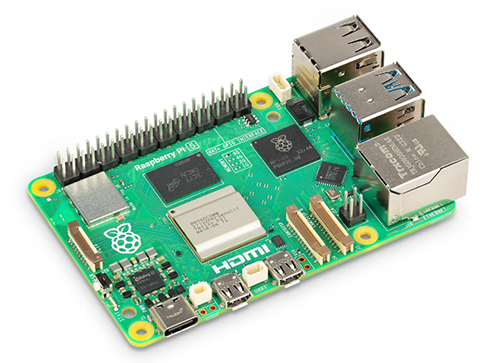
SC1112

Raspberry Pi

$79.61 - $86.40

IN STOCK 10266
Buy

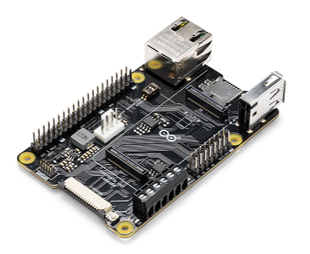
ASX00049

Arduino

* $39.41 - * $44.41

IN STOCK 3132
Buy

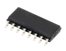
AD96685BRZ

Analog Devices Inc.

$1.72 - * $11.79

IN STOCK 4921
Buy

Reference Designs

RD006

Wurth Elektronik

RD006 - 3 W Dual-output isolated auxiliary supply for communication interfaces and measurement systems

CN0583

Analog Devices Inc.

Multistandard Micropower Verified Smoke Detection System-on-Module

Technical Resources

EVALUATION KITS

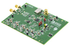
EVAL-AD7124-8SDZ

Analog Devices Inc.

$71.02 - * $75.98

IN STOCK 808
Buy
View All