Top Manufacturers
Stock

Displaying 1141 - 1160 of 5439

Evaluation Kits from Analog Devices Inc.

108355-HMC409LP4

Analog Devices Inc.
The HMC409LP4(E) is a high efficiency GaAs InGaP HBT MMIC Power amplifier operating from 3.3 to 3.8 GHz. The amplifier is packaged in a low cost, leadless SMT package. Utilizing a minimum of external components the amplifier provides 31 dB of gain and +32.5 dBm of saturated power from a +5V supply voltage. The power control (Vpd) can be used for full power down or RF output power/current control. For +22 dBm OFDM output power (64 QAM, 54 Mbps), the HMC409LP4(E) achieves an error vector magnitude (EVM) of 2%, meeting WiMAX 802.16 linearity requirements.Applications WiMAX 802.16 Fixed Wireless Access Wireless Local Loop

110227-HMC510LP5

Analog Devices Inc.
The HMC510LP5(E) is a GaAs InGaP Heterojunction Bipolar Transistor (HBT) MMIC VCO. The HMC510LP5(E) integrates resonators, negative resistance devices, varactor diodes and feature half frequency and divide-by-4 outputs. The VCO?s phase noise performance is excellent over temperature, shock, and process due to the oscillator?s monolithic structure. Power output is +13 dBm typical from a +5V supply voltage. The prescaler and RF/2 functions can be disabled to conserve current if not required. The voltage controlled oscillator is packaged in a leadless QFN 5?5 mm surface mount package, and requires no external matching components.APPLICATIONS Point-to-Point/Multi-Point Radio? Test Equipment & Industrial Controls? SATCOM? Military End-Use

110227-HMC512LP5

Analog Devices Inc.
The HMC512LP5(E) is a GaAs InGaP Herterojunction Bipolar Transistor (HBT) MMIC VCOs. The HMC512LP5(E) integrates resonators, negative resistance devices, varactor diodes and feature half frequency and divide-by-4 outputs. The VCO's phase noise performance is excellent over temperature, shock and process due to the oscillator's monolithic structure. Power output is +9 dBm typical from a +5V supply voltage. The prescaler and RF/2 functions can be disabled to conserve current if not required. The voltage cont-rolled oscillator is packaged in a leadless QFN 5x5 mm surface mount package, and requires no external matching components.APPLICATIONS Point-to-Point Radios? Point-to-Multi-Point Radios Test Equipment & Industrial Controls? SATCOM Military End-Use

110227-HMC584LP5

Analog Devices Inc.
The HMC584LP5(E) is a GaAs InGaP Heterojunction Bipolar Transistor (HBT) MMIC VCO. The HMC584LP5(E) integrates resonators, negative resistance devices, varactor diodes and feature half frequency and divide-by-4 outputs. The VCO?s phase noise performance is excellent over temperature, shock, and process due to the oscillator?s monolithic structure. Power output is +10 dBm typical from a +5V supply voltage. The prescaler and RF/2 functions can be disabled to conserve current if not required. The voltage controlled oscillator is packaged in a leadless QFN 5x5 mm surface mount package, and requires no external matching components.APPLICATIONS Point to Point/Multipoint Radio Test Equipment & Industrial Controls SATCOM Military End-Use

112585-HMC376LP3

Analog Devices Inc.
The HMC376LP3 & HMC376LP3E are GaAs PHEMT MMIC Low Noise Amplifiers that are ideal for GSM & CDMA cellular basestation front-end receivers operating between 700 and 1000 MHz. The amplifier has been optimized to provide 0.7 dB noise figure, 15 dB gain and +36 dBm output IP3 from a single supply of +5V. The HMC376LP3(E) feature an externally adjustable supply current which allows the designer to tailor the linearity performance of the LNA for each application. For applications which require improved noise figure, please see the HMC617LP3(E).Applications Cellular/3G Infrastructure Base Stations & Repeaters CDMA, W-CDMA, & TD-SCDMA Private Land Mobile Radio GSM/GPRS & EDGE UHF Reallocation Applications

113589-HMC3587LP3B

Analog Devices Inc.
The HMC3587LP 3BE is a HBT Gain Block MMI C amplifier covering 4 GHz to 10 GHz and packaged in a 3x3 mm plastic QFN SM T package. This versatile amplifier can be used as a cascadable IF or RF gain stage in 50 Ohm applications. The HMC3587LP 3BE delivers 14.5 dB gain, and +13 dBm output P1dB with only 3.5 dB noise figure.Applications Cellular / PCS / 3G Fixed Wireless & WLAN CATV, Cable Modem & DBS Microwave Radio & Test Equipment IF & RF Applications

115556-HMC561LP3

Analog Devices Inc.
The HMC561LP3(E) is a x2 active broadband frequency multiplier utilizing GaAs PHEMT technology in a leadless RoHS compliant SMT package. When driven by a +5 dBm signal, the multiplier provides +14 dBm typical output power from 8 to 21 GHz and the Fo and 3Fo isolations are 15 dBc at 16 GHz. The HMC561LP3(E) is ideal for use in LO multiplier chains for Pt to Pt & VSAT Radios yielding reduced parts count vs. traditional approaches.The low additive SSB Phase Noise of -139 dBc/Hz at 100 kHz offset helps maintain good system noise performance. The RoHS packaged HMC561LP3(E) eliminates the need for wire bonding, and allows the use of surface mount manufacturing techniques.APPLICATIONS Clock Generation Applications:? SONET OC-192 & SDH STM-64? Point-to-Point & VSAT Radios? Test Instrumentation? Military & Space

115585-HMC680LP4

Analog Devices Inc.
The HMC680LP4(E) is a digitally controlled variable gain amplifier which operates from 30 to 400 MHz, and can be programmed to provide -4 dB to +19 dB of gain, in 1 dB steps. The HMC680LP4(E) delivers noise figure of 5 dB in its maximum gain state, with output IP3 of up to +40 dBm in any state. This high linearity DVGA also provides a differential RF output which can be used to interface directly with SAW filters in Tx and Rx applications, and with digital to analog converters in Rx chains. The HMC680LP4(E) is housed in a RoHS compliant 4x4 mm QFN leadless package, and is CMOS/ TTL compatible.Applications Cellular/3G Infrastructure WiBro / WiMAX / 4G Microwave Radio & VSAT Test Equipment and Sensors IF & RF Applications?

AD9645-125EBZ

Analog Devices Inc.
The AD9645 is a dual, 14-bit, 80 MSPS/125 MSPS analog-to-digital converter (ADC) with an on-chip sample-and-hold circuit designed for low cost, low power, small size, and ease of use. The product operates at a conversion rate of up to 125 MSPS and is optimized for outstanding dynamic performance and low power in applications where a small package size is critical.The ADC requires a single 1.8 V power supply and LVPECL-/ CMOS-/LVDS-compatible sample rate clock for full performanceoperation. No external reference or driver components arerequired for many applications. The ADC automatically multiplies the sample rate clock for theappropriate LVDS serial data rate. A data clock output (DCO) for capturing data on the output and a frame clock output (FCO) forsignaling a new output byte are provided. Individual channelpower-down is supported; the AD9645 typically consumes lessthan 2 mW in the full power-down state. The ADC providesseveral features designed to maximize flexibility and minimize system cost, such as programmable output clock and data alignment and digital test pattern generation. The available digital test patterns include built-in deterministic and pseudorandom patterns, along with custom user-defined test patterns entered via the serial port interface (SPI). The AD9645 is available in a RoHS-compliant, 32-lead LFCSP. It is specified over the industrial temperature range of ?40?C to +85?C. This product is protected by a U.S. patent.PRODUCT HIGHLIGHTS Small Footprint. Two ADCs are contained in a small, spacesaving package. Low Power. The AD9645 uses 122 mW/channel at 125 MSPS with scalable power options. Pin Compatibility with the AD9635, a 12-Bit Dual ADC. Ease of Use. A data clock output (DCO) operates at frequencies of up to 500 MHz and supports double data rate (DDR) operation. User Flexibility. The SPI control offers a wide range of flexible features to meet specific system requirements.APPLICATIONS Communications Diversity radio systems Multimode digital receivers GSM, EDGE, W-CDMA, LTE, CDMA2000, WiMAX, TD-SCDMA I/Q demodulation systems Smart antenna systems Broadband data applications Battery-powered instruments Hand held scope meters Portable medical imaging and ultrasound Radar/LIDAR

AD9695-625EBZ

Analog Devices Inc.
The AD9695 is a dual, 14-bit, 1300 MSPS/625 MSPS analog-to-digital converter (ADC). The device has an on-chip buffer and a sample-and-hold circuit designed for low power, small size, and ease of use. This product is designed to support communications applications capable of direct sampling wide bandwidth analog signals of up to 2 GHz. The ?3 dB bandwidth of the ADC input is 2 GHz. The AD9695 is optimized for wide input bandwidth, high sampling rate, excellent linearity, and low power in a small package.The dual ADC cores feature a multistage, differential pipelined architecture with integrated output error correction logic. Each ADC features wide bandwidth inputs supporting a variety of user-selectable input ranges. An integrated voltage reference eases design considerations. The analog input and clock signals are differential inputs. The ADC data outputs are internally connected to four digital downconverters (DDCs) through a crossbar mux. Each DDC consists of multiple signal processing stages: a 48-bit frequency translator (numerically controlled oscillator (NCO)), and decimation filters. The NCO has the option to select up to 16 preset bands over the general-purpose input/output (GPIO) pins, or use a coherent fast frequency hopping mechanism for band selection. Operation of the AD9695 between the DDC modes is selectable via SPI-programmable profiles.In addition to the DDC blocks, the AD9695 has several functions that simplify the automatic gain control (AGC) function in a communications receiver. The programmable threshold detector allows monitoring of the incoming signal power using the fast detect control bits in Register 0x0245 of the ADC. If the input signal level exceeds the programmable threshold, the fast detect indicator goes high. Because this threshold indicator has low latency, the user can quickly turn down the system gain to avoid an overrange condition at the ADC input. In addition to the fast detect outputs, the AD9695 also offers signal monitoring capability. The signal monitoring block provides additional information about the signal being digitized by the ADC.The user can configure the Subclasss 1 JESD204B-based high speed serialized output using either one lane, two lanes, or four lanes, depending on the DDC configuration and the acceptable lane rate of the receiving logic device. Multidevice synchronization is supported through the SYSREF? and SYNCINB? input pins.The AD9695 has flexible power-down options that allow significant power savings when desired. All of these features can be programmed using a 3-wire serial port interface (SPI) and or PDWN/STBY pin.The AD9695 is available in a Pb-free, 64-lead LFCSP and is specified over the ?40?C to +105?C junction temperature range. This product may be protected by one or more U.S. or international patents.Note that, throughout this data sheet, multifunction pins, such as FD_A/GPIO_A0, are referred to either by the entire pin name or by a single function of the pin, for example, FD_A, when only that function is relevant.Product Highlights Low power consumption per channel. JESD204B lane rate support up to 16 Gbps. Wide, full power bandwidth supports intermediate frequency (IF) sampling of signals up to 2 GHz. Buffered inputs ease filter design and implementation. Four integrated wideband decimation filters and NCO blocks supporting multiband receivers. Programmable fast overrange detection. On-chip temperature diode for system thermal management.Applications Communications Diversity multiband, multimode digital receivers 3G/4G, TD-SCDMA, WCDMA, GSM, LTE General-purpose software radios Ultrawideband satellite receiver Instrumentation Oscilloscopes Spectrum analyzers Network analyzers Integrated RF test solutions Radars Electronic support measures, electronic counter measures, and electronic counter-counter measures High speed data acquisition systems DOCSIS 3.0 CMTS upstream receive paths Hybrid fiber coaxial digital reverse path receivers Wideband digital predistortion

AD9706-DPG2-EBZ

Analog Devices Inc.
The AD9704/AD9705/AD9706/AD9707 are the fourth-generation family in the TxDAC series of high performance, CMOS digital-to-analog converters (DACs). This pin-compatible, 8-/10-/12-/14-bit resolution family is optimized for low power operation, while maintaining excellent dynamic performance. The AD9704/AD9705/AD9706/AD9707 family is pin-compatible with the AD9748/AD9740/AD9742/AD9744 family of TxDAC converters and is specifically optimized for the transmit signal path of communication systems. All of the devices share the same interface, LFCSP package, and pinout, providing an upward or downward component selection path based on performance, resolution, and cost. The AD9704/AD9705/AD9706/AD9707 offers exceptional ac and dc performance, while supporting update rates up to 175 MSPS.The flexible power supply operating range of 1.7 V to 3.6 V and low power dissipation of the AD9704/AD9705/AD9706/AD9707 parts make them well suited for portable and low power applications.Power dissipation of the AD9704/AD9705/AD9706/AD9707 can be reduced to 15 mW, with a small trade-off in performance, by lowering the full-scale current output. In addition, a power-down mode reduces the standby power dissipation to approximately 2.2 mW.The AD9704/AD9705/AD9706/AD9707 has an optional serial peripheral interface (SPI?) that provides a higher level of programmability to enhance performance of the DAC. An adjustable output, common-mode feature allows for easy interfacing to other components that require common modes from 0 V to 1.2 V.Edge-triggered input latches and a 1.0 V temperature-compensated band gap reference have been integrated to provide a complete, monolithic DAC solution. The digital inputs support 1.8 V and 3.3 V CMOS logic families.PRODUCT HIGHLIGHTS Pin Compatible. The AD9704/AD9705/AD9706/AD9707 line of TxDAC?converters is pin-compatible with theAD9748/AD9740/AD9742/AD9744 TxDAC line (LFCSP package). Low Power. Complete CMOS DAC operates on a single supply of 3.6 V down to 1.7 V, consuming 50 mW (3.3 V) and 12 mW (1.8 V). The DAC full-scale current can be reduced for lower power operation. Sleep and power-down modes are provided for low power idle periods. Self-Calibration. Self-calibration enables true 14-bit INL and DNL performance in the AD9707. Twos Complement/Binary Data Coding Support. Data input supports twos complement or straight binary data coding. Flexible Clock Input. A selectable high speed, single-ended,and differential CMOS clock input supports 175 MSPS conversion rate. Device Configuration. Device can be configured through pin strapping, and SPI control offers a higher level of programmability. Easy Interfacing to Other Components. Adjustable common-mode output allows for easy interfacing to other signal chain components that accept common-mode levels from 0 V to 1.2 V. On-Chip Voltage Reference. The AD9704/AD9705/AD9706/AD9707 include a 1.0 V temperature-compensated band gap voltage reference. Industry-Standard 32-Lead LFCSP Package.

AD9708-EBZ

Analog Devices Inc.
The AD9708 is the 8-bit resolution member of the TxDAC? series of high performance, low power CMOS digital-to-analog converters (DACs). The TxDAC? family, which consists of pin compatible 8-, 10-, 12-, and 14-bit DACs, was specifically optimized for the transmit signal path of communication systems. All of the devices share the same interface options, small outline package and pinout, thus providing an upward or downward component selection path based on performance, resolution and cost. The AD9708 offers exceptional ac and dc performance while supporting update rates up to 125 MSPS.The AD9708's flexible single-supply operating range of 2.7 V to 5.5 V and low power dissipation are well suited for portable and low power applications. Its power dissipation can be further reduced to 45 mW, without a significant degradation in performance, by lowering the full-scale current output. In addition, a power-down mode reduces the standby power dissipation to approximately 20 mW.The AD9708 is manufactured on an advanced CMOS process. A segmented current source architecture is combined with a proprietary switching technique to reduce spurious components and enhance dynamic performance. Edge-triggered input latches and a temperature compensated bandgap reference have been integrated to provide a complete monolithic DAC solution. Flexible supply options support +3 V and +5 V CMOS logic families.The AD9708 is a current-output DAC with a nominal full-scale output current of 20 mA and > 100 k Ohms output impedance.Differential current outputs are provided to support single-ended or differential applications. The current outputs may be directly tied to an output resistor to provide two complementary, single-ended voltage outputs. The output voltage compliance range is 1.25 V.The AD9708 contains a 1.2 V on-chip reference and reference control amplifier, which allows the full-scale output current to be simply set by a single resistor. The AD9708 can be driven by a variety of external reference voltages. The AD9708's full-scale current can be adjusted over a 2 mA to 20 mA range without any degradation in dynamic performance. Thus, the AD9708 may operate at reduced power levels or be adjusted over a 20 dB range to provide additional gain ranging capabilities.The AD9708 is available in a 28-pin SOIC package. It is specified for operation over the industrial temperature range.

AD9735-DPG2-EBZ

Analog Devices Inc.
The AD9736, AD9735, and AD9734 are high performance, high frequency DACs that provide sample rates of up to 1200 MSPS, permitting multicarrier generation up to their Nyquist frequency. The AD9736 is the 14-bit member of the family, while the AD9735 and the AD9734 are the 12-bit and 10-bit members, respectively. They include a serial peripheral interface (SPI) port that provides for programming of many internal parameters and enables readback of status registers.A reduced-specification LVDS interface is utilized to achieve the high sample rate. The output current can be programmed over a range of 8.66 mA to 31.66 mA. The AD973x family is manufactured on a 0.18 ?m CMOS process and operates from 1.8 V and 3.3 V supplies for a total power consumption of 380 mW in bypass mode. It is supplied in a 160-lead chip scale ball grid array for reduced package parasitics.Product Highlights Low noise and intermodulation distortion (IMD) features enable high quality synthesis of wideband signals at intermediate frequencies up to 600 MHz. Double data rate (DDR) LVDS data receivers support the maximum conversion rate of 1200 MSPS. Direct pin programmability of basic functions or SPI port access offers complete control of all AD973x family functions. Manufactured on a CMOS process, the AD973x family uses a proprietary switching technique that enhances dynamic performance. The current output(s) of the AD9736 family are easily configured for single-ended or differential circuit topologies.Applications Broadband communications systems Cellular infrastructure (digital predistortion) Point-to-point wireless CMTS/VOD Instrumentation, automatic test equipment Radar, avionics

AD9736-DPG2-EBZ

Analog Devices Inc.
The AD9736, AD9735, and AD9734 are high performance, high frequency DACs that provide sample rates of up to 1200 MSPS, permitting multicarrier generation up to their Nyquist frequency. The AD9736 is the 14-bit member of the family, while the AD9735 and the AD9734 are the 12-bit and 10-bit members, respectively. They include a serial peripheral interface (SPI) port that provides for programming of many internal parameters and enables readback of status registers.A reduced-specification LVDS interface is utilized to achieve the high sample rate. The output current can be programmed over a range of 8.66 mA to 31.66 mA. The AD973x family is manufactured on a 0.18 ?m CMOS process and operates from 1.8 V and 3.3 V supplies for a total power consumption of 380 mW in bypass mode. It is supplied in a 160-lead chip scale ball grid array for reduced package parasitics.Product Highlights Low noise and intermodulation distortion (IMD) features enable high quality synthesis of wideband signals at intermediate frequencies up to 600 MHz. Double data rate (DDR) LVDS data receivers support the maximum conversion rate of 1200 MSPS. Direct pin programmability of basic functions or SPI port access offers complete control of all AD973x family functions. Manufactured on a CMOS process, the AD973x family uses a proprietary switching technique that enhances dynamic performance. The current output(s) of the AD9736 family are easily configured for single-ended or differential circuit topologies.Applications Broadband communications systems Cellular infrastructure(digital predistortion) Point-to-point wireless CMTS/VOD Instrumentation, automatic test equipment Radar, avionics

AD9748-FMC-EBZ

Analog Devices Inc.
The AD97481 is an 8-bit resolution, wideband, third generation member of the TxDAC series of high performance, low power CMOS digital-to-analog converters (DACs). The TxDAC family, consisting of pin-compatible 8-, 10-, 12-, and 14-bit DACs, is specifically optimized for the transmit signal path of communication systems. All of the devices share the same interface options, small outline package, and pinout, providing an upward or downward component selection path based on performance, resolution, and cost. The AD9748 offers exceptional ac and dc performance while supporting update rates up to 210 MSPS. The AD9748?s low power dissipation makes it well suited for portable and low power applications. Its power dissipation can be further reduced to 60 mW with a slight degradation in performance by lowering the full-scale current output. In addition, a power-down mode reduces the standby power dissipation to approximately 15 mW. A segmented current source architecture is combined with a proprietary switching technique to reduce spurious components and enhance dynamic performance. Edge-triggered input latches and a 1.2 V temperature-compensated band gap reference have been integrated to provide a complete monolithic DAC solution. The digital inputs support 3 V CMOS logic families. PRODUCT HIGHLIGHTS 32-lead LFCSP. The AD9748 is the 8-bit member of the pin-compatible TxDAC family, which offers excellent INL and DNL performance. Differential or single-ended clock input (LVPECL or CMOS), supports 210 MSPS conversion rate. Data input supports twos complement or straight binary data coding. Low power: Complete CMOS DAC function operates on 135 mW from a 2.7 V to 3.6 V single supply. The DAC full-scale current can be reduced for lower power operation, and a sleep mode is provided for low power idle periods. On-chip voltage reference: The AD9748 includes a 1.2 V temperature-compensated band gap voltage reference.?APPLICATIONS Communications Direct digital synthesis (DSS) Instrumentation

AD9761-EBZ

Analog Devices Inc.
The AD9761 is a complete dual channel, high speed, 10-bitCMOS DAC. The AD9761 has been developed specifically foruse in wide bandwidth communication applications (e.g., spreadspectrum) where digital I and Q information is being processedduring transmit operations. It integrates two 10-bit, 40 MSPSDACs, dual 2x interpolation filters, a voltage reference, anddigital input interface circuitry. The AD9761 supports a20 MSPS per channel input data rate that is then interpolatedby 2x up to 40 MSPS before simultaneously updating eachDAC.The interleaved I and Q input data stream is presented to thedigital interface circuitry, which consists of I and Q latches as wellas some additional control logic. The data is de-interleaved backinto its original I and Q data. An on-chip state machine ensures theproper pairing of I and Q data. The data output from each latch isthen processed by a 2x digital interpolation filter that eases thereconstruction filter requirements. The interpolated output of eachfilter serves as the input of their respective 10-bit DAC.The DACs utilize a segmented current source architecture combinedwith a proprietary switching technique to reduce glitchenergy and to maximize dynamic accuracy. Each DAC providesdifferential current output thus supporting single-ended ordifferential applications. Both DACs are simultaneously updatedand provide a nominal full-scale current of 10 mA. Also,the full-scale currents between each DAC are matched to within0.07 dB (i.e., 0.75%), thus eliminating the need for additionalgain calibration circuitry.The AD9761 is manufactured on an advanced low cost CMOSprocess. It operates from a single supply of 2.7 V to 5.5 V andconsumes 200 mW of power. To make the AD9761 complete italso offers an internal 1.20 V temperature-compensated bandgapreference.PRODUCT HIGHLIGHTS Dual 10-Bit, 40 MSPS DACs A pair of high performance 40 MSPS DACs optimized for low distortion performance provide for flexible transmission of I and Q information. 2x Digital Interpolation Filters Dual matching FIR interpolation filters with 62.5 dB stopband rejection precede each DAC input, thus reducing the DACs? reconstruction filter requirements. Low Power Complete CMOS dual DAC function operates on a low 200 mW on a single supply from 3 V to 5.5 V. The DAC full-scale current can be reduced for lower power operation, and a sleep mode is provided for power reduction during idle periods. On-Chip Voltage Reference The AD9761 includes a 1.20 V temperature-compensated band gap voltage reference. Single 10-Bit Digital Input Bus The AD9761 features a flexible digital interface that allows each DAC to be addressed in a variety of ways including different update rates. Small Package The AD9761 offers the complete integrated function in a compact 28-lead SSOP package. Product Family The AD9761 Dual Transmit DAC has a pair of Dual Receive ADC companion products, the AD9281 (8 bits) and AD9201 (10 bits).

AD9767-KIT-EBZ

Analog Devices Inc.
The AD9763/AD9765/AD9767 are dual-port, high speed, 2-channel, 10-/12-/14-bit CMOS DACs. Each part integratestwo high quality TxDAC+? cores, a voltage reference, and digital interface circuitry into a small 48-lead LQFP. The AD9763/AD9765/AD9767 offer exceptional ac and dc performancewhile supporting update rates of up to 125 MSPS.The AD9763/AD9765/AD9767 have been optimized forprocessing I and Q data in communications applications. Thedigital interface consists of two double-buffered latches as well as control logic. Separate write inputs allow data to be written to the two DAC ports independent of one another. Separate clocks control the update rate of the DACs.A mode control pin allows the AD9763/AD9765/AD9767 to interface to two separate data ports, or to a single interleavedhigh speed data port. In interleaving mode, the input datastream is demuxed into its original I and Q data and then latched. The I and Q data is then converted by the two DACsand updated at half the input data rate.The GAINCTRL pin allows two modes for setting the full-scale current (IOUTFS) of the two DACs. IOUTFS for each DAC can be set independently using two external resistors, or IOUTFS for both DACs can be set by using a single external resistor. See theGain Control Mode section for important date codeinformation on this feature.The DACs utilize a segmented current source architecturecombined with a proprietary switching technique to reduce glitch energy and maximize dynamic accuracy. Each DAC providesdifferential current output, thus supporting single-ended or differential applications. Both DACs of the AD9763, AD9765, or AD9767 can be simultaneously updated and can provide anominal full-scale current of 20 mA. The full-scale currentsbetween each DAC are matched to within 0.1%.The AD9763/AD9765/AD9767 are manufactured on anadvanced, low cost CMOS process. They operate from a singlesupply of 3.3 V to 5 V and consume 380 mW of power.Product HighlightsThe AD9763/AD9765/AD9767 are members of a pin-compatible family of dual TxDACs providing 8-, 10-, 12-, and 14-bit resolution.Dual 10-/12-/14-Bit, 125 MSPS DACs. A pair of high performance DACs for each part is optimized for low distortion performance and provides flexible transmission of I and Q information.Matching. Gain matching is typically 0.1% of full scale, and offset error is better than 0.02%.Low Power. Complete CMOS dual DAC function operates on 380 mW from a 3.3 V to 5 V single supply. The DAC full-scalecurrent can be reduced for lower power operation, and a sleepmode is provided for low power idle periods.On-Chip Voltage Reference. The AD9763/AD9765/AD9767each include a 1.20 V temperature-compensated band gapvoltage reference.Dual 10-/12-/14-Bit Inputs. The AD9763/AD9765/AD9767each feature a flexible dual-port interface, allowing dual orinterleaved input data.ApplicationsCommunicationsBase stationsDigital synthesisQuadrature modulation3D ultrasound

AD9913/PCBZ

Analog Devices Inc.
The AD9913 is a complete direct digital synthesizer (DDS) designed to meet the stringent power consumption limits of portable, handheld, and battery-powered equipment. The AD9913 features a 10-bit digital-to-analog converter (DAC) operating up to 250 MSPS. The AD9913 uses advanced DDS technology, coupled with an internal high speed, high performance DAC to form a complete, digitally-programmable, high frequency synthesizer capable of generating a frequency agile analog output sinusoidal waveform at up to 100 MHz.The AD9913 provides fast frequency hopping and fine tuning resolution. The AD9913 also offers fine resolution phase offset control. Control words are loaded into the AD9913 through the serial or parallel I/O port. The AD9913 also supports a user-defined linear sweep mode of operation for generating highly linearized swept waveforms of frequency. To support various methods of generating a system clock, the AD9913 includes an oscillator, allowing a simple crystal to be used as the frequency reference, as well as a high speed clock multiplier to convert the reference clock frequency up to the full system clock rate. For power saving considerations, many of the individual blocks of the AD9913 can be powered down when not in use.The AD9913 operates over the extended industrial temperature range of ?40?C to +85?C.APPLICATIONS Portable and handheld equipment Agile LO frequency synthesis Programmable clock generator FM chirp source for radar and scanning systems

AD9963-EBZ

Analog Devices Inc.
The AD9961/AD9963 are pin-compatible, 10-/12-bit, lowpower MxFE? converters that provide two ADC channels withsample rates of 100 MSPS and two DAC channels with samplerates to 170 MSPS. These converters are optimized for transmit and receive signal paths of communication systems requiring lowpower and low cost. The digital interfaces provide flexibleclocking options. The transmit is configurable for 1?, 2?, 4?,and 8? interpolation. The receive path has a bypassable 2?decimating low-pass filter.The AD9961 and AD9963 have five auxiliary analog channels.Three are inputs to a 12-bit ADC. Two of these inputs can beconfigured as outputs by enabling 10-bit DACs. The other two channels are dedicated outputs from two independent 12-bit DACs.The high level of integrated functionality, small size, and lowpower dissipation of the AD9961/AD9963 make them well-suited for portable and low power applications.APPLICATIONS Wireless infrastructure Picocell, femtocell basestations Medical instrumentation Ultrasound AFE Portable instrumentation Signal generators, signal analyzers

ADA4432-1BCP-EBZ

Analog Devices Inc.
The ADA4432-1 is a single-ended output fully integrated video reconstruction filter that combines overvoltage protection (short-to-battery [STB] protection) and short-to-ground (STG) protection on the outputs, with excellent video specifications and low power consumption. The combination of STB protection and robust ESD tolerance allows the ADA4432-1 to provide superior protection in the hostile automotive environment.The ADA4432-1 is a single-ended input/single-ended output video filter capable of driving long back-terminated cables.The short-to-battery protection integrated into the ADA4432-1 protects against both dc and transient overvoltage events, caused by an accidental short to a battery voltage up to 18 V. The Analog Devices, Inc., short-to-battery protection eliminates the need for large output coupling capacitors and other complicated circuits used to protect standard video amplifiers, saving space and cost.The ADA4432-1 features a high-order filter with ?3 dB cutoff frequency response at 10 MHz and 45 dB of rejection at 27 MHz. The ADA4432-1 features an internally fixed gain of 2 V/V. This makes the ADA4432-1 ideal for SD video applications, including NTSC and PAL.The ADA4432-1 operatea on single supplies as low as 2.6 V and as high as 3.6 V while providing the dynamic range required by the most demanding video systems.The ADA4432-1 is offered in an 8-lead, 3 mm ? 3 mm LFCSP package and a 6-lead SOT-23 package. It is rated for operation over the wide automotive temperature range of ?40?C to +125?C.Appplications Automotive rearview cameras Automotive video electronic control units (ECUs) Surveillance video systems

Displaying 1141 - 1160 of 5439

Latest Parts

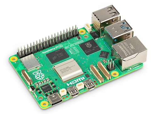
SC1112

Raspberry Pi

$80.00 - $80.01

IN STOCK 4959
Buy

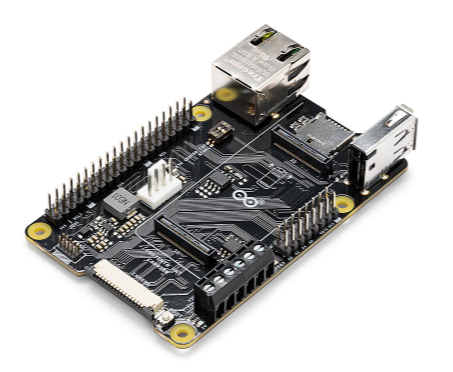
ASX00049

Arduino

* $33.69 - * $42.25

IN STOCK 3008
Buy
IN STOCK 4682
Buy

Reference Designs

RD006

Wurth Elektronik

RD006 - 3 W Dual-output isolated auxiliary supply for communication interfaces and measurement systems

CN0583

Analog Devices Inc.

Multistandard Micropower Verified Smoke Detection System-on-Module

Technical Resources

EVALUATION KITS

EVAL-AD7124-8SDZ

Analog Devices Inc.

$63.71 - * $75.43

IN STOCK 794
Buy
View All