
EV1HMC7911LP5
Analog Devices Inc.The HMC7911 is a compact gallium arsenide (GaAs), pseudomorphic(pHEMT), monolithic microwave integrated circuit(MMIC) upconverter in a RoHS compliant, low stress, injectionmolded plastic LFCSP package that operates from 17 GHz to20 GHz. This device provides a small signal conversion gain of18 dB with 30 dBc of sideband rejection. The HMC7911 uses avariable gain amplifier preceded by an in-phase/quadrature (I/Q)mixer that is driven by an active 2? local oscillator (LO) multiplier.IF1 and IF2 mixer inputs are provided, and an external 90? hybridis needed to select the required sideband. The I/Q mixer topologyreduces the need for filtering of the unwanted sideband. TheHMC7911 is a much smaller alternative to hybrid style singlesideband (SSB) upconverter assemblies, and it eliminates theneed for wire bonding by allowing the use of surface-mountmanufacturing techniques.Applications Point to point and point to multipoint radios Military radars, electronic warfare (EW), and electronic intelligence (ELINT) Satellite communications Sensors

EV1HMC7912LP5
Analog Devices Inc.The HMC7912 is a compact, gallium arsenide (GaAs), pseudomorphic(pHEMT), monolithic microwave integrated circuit(MMIC) upconverter in a RoHS compliant, low stress, injectionmolded plastic LFCSP package that operates from 21 GHz to24 GHz. This device provides a small signal conversion gain of15 dB with 22 dBc of sideband rejection. The HMC7912 uses avariable gain amplifier preceded by an in-phase/quadrature (I/Q)mixer that is driven by an active 2? LO multiplier. IF1 and IF2mixer inputs are provided, and an external 90? hybrid is needed toselect the required sideband. The I/Q mixer topology reducesthe need for filtering of the unwanted sideband. The HMC7912is a much smaller alternative to hybrid style single sideband (SSB)upconverter assemblies, and it eliminates the need for wirebonding by allowing the use of surface-mount manufacturingtechniques.Applications Point to point and point to multipoint radios Military radars, electronic warfare (EW), and electronic intelligence (ELINT) Satellite communications Sensors

EV1HMC8412LP2F
Analog Devices Inc.The HMC8412 is a gallium arsenide (GaAs), monolithic microwave integrated circuit (MMIC), pseudomorphic high electron mobility transistor (pHEMT), low noise wideband amplifier that operates from 0.4 GHz to 11 GHz. The HMC8412 provides a typical gain of 15.5 dB, a 1.4 dB typical noise figure, and a typical output third-order intercept (OIP3) of ?33 dBm, requiring only 60 mA from a 5 V drain supply voltage. The saturated output power (PSAT) of ?20.5 dBm typical enables the low noise amplifier (LNA) to function as a local oscillator (LO) driver for many Analog Devices, Inc., balanced, inphase and quadrature (I/Q) or image rejection mixers. The HMC8412 also features inputs and outputs that are internally matched to 50 ?, making the device ideal for surface-mount technology (SMT)-based, high capacity microwave radio applications. The HMC8412 is housed in an RoHS-compliant, 2 mm ? 2 mm, 6-lead LFCSP.APPLICATIONS Test instrumentation Telecommunications Military radar and communication Electronic warfare Aerospace

EV1HMC936ALP6
Analog Devices Inc.The HMC936ALP6E is a 6-bit digital phase shifterwhich is rated from 1.2 to 1.4 GHz, providing 360degrees of phase coverage, with a LSB of 5.625degrees. The HMC936ALP6E features very low RMSphase error of 1.2 degrees and extremely low inser-tionloss variation of ?0.5 dB across all phase states. Thishigh accuracy phase shifter is controlled with positivecontrol logic of 0/+5V and requires no negative supplyvoltage. The HMC936ALP6E is housed in a compact6x6 mm plastic leadless SMT package and is internallymatched to 50 Ohms with no external components.Applications EW receivers? Weather and military radar Satellite communications Beamforming modules Phase cancellation

EV-21564L-SOM
Analog Devices Inc.Reaching speeds of up to 1 GHz, the ADSP-2159x processors are members of the SHARC? family of products. The ADSP-2159x processor is a dual-SHARC+? core DSP that doubles the audio performance of its single-SHARC+ core ADSP-2156x predecessor while maintaining pin-compatibility to it in the BGA package, providing design scalability from 400 MHz (ADSP-21566) to 2 GHz (ADSP-21593).The ADSP-2159x SHARC processors are members of the SIMD SHARC family of digital signal processors (DSPs) that feature Analog Devices, Inc., Super Harvard Architecture. These 32-bit/40-bit/64-bit floating-point processors are optimized for high performance audio/floating-point applications with large on-chip static random-access memory (SRAM), multiple internal buses that eliminate input/output (I/O) bottlenecks, and innovative digital audio interfaces (DAI). New additions to the SHARC+ core include cache enhancements and branch prediction, while maintaining instruction set compatibility to previous SHARC products.By integrating a rich set of industry-leading system peripherals and memory (see Table 1 in the data sheet), the SHARC+ processor is the platform of choice for applications that require programmability similar to reduced instruction set computing (RISC), multimedia support, and leading edge signal processing in one integrated package. These applications span a wide array of markets, including automotive, professional audio, and industrial-based applications that require high floating-point performance.APPLICATIONS Automotive: audio amplifier, head unit, ANC/RNC, rear seat entertainment, digital cockpit, ADAS Consumer & Professional Audio: speakers, sound bars, AVRs, conferencing systems, mixing consoles, microphone arrays, headphones
EV-21564-SOM
Analog Devices Inc.Reaching speeds of up to 1 GHz, the ADSP-2159x processors are members of the SHARC? family of products. The ADSP-2159x processor is a dual-SHARC+? core DSP that doubles the audio performance of its single-SHARC+ core ADSP-2156x predecessor while maintaining pin-compatibility to it in the BGA package, providing design scalability from 400 MHz (ADSP-21566) to 2 GHz (ADSP-21593).The ADSP-2159x SHARC processors are members of the SIMD SHARC family of digital signal processors (DSPs) that feature Analog Devices, Inc., Super Harvard Architecture. These 32-bit/40-bit/64-bit floating-point processors are optimized for high performance audio/floating-point applications with large on-chip static random-access memory (SRAM), multiple internal buses that eliminate input/output (I/O) bottlenecks, and innovative digital audio interfaces (DAI). New additions to the SHARC+ core include cache enhancements and branch prediction, while maintaining instruction set compatibility to previous SHARC products.By integrating a rich set of industry-leading system peripherals and memory (see Table 1 in the data sheet), the SHARC+ processor is the platform of choice for applications that require programmability similar to reduced instruction set computing (RISC), multimedia support, and leading edge signal processing in one integrated package. These applications span a wide array of markets, including automotive, professional audio, and industrial-based applications that require high floating-point performance.APPLICATIONS Automotive: audio amplifier, head unit, ANC/RNC, rear seat entertainment, digital cockpit, ADAS Consumer & Professional Audio: speakers, sound bars, AVRs, conferencing systems, mixing consoles, microphone arrays, headphones

EV-AD5544/45SDZ
Analog Devices Inc.The AD5544/AD5554 quad, 16-/14-bit, current output, digital-to-analog converters (DACs) are designed to operate from 2.7 V to 5.5 V supply range.The applied external reference input voltage (VREFX) determines the full-scale output current. Integrated feedback resistors (RFB) provide temperature-tracking, full-scale voltage outputs when combined with an external I-to-V precision amplifier.A double-buffered serial data interface offers high speed, 3-wire, SPI- and microcontroller-compatible inputs using serial data in (SDI), a chip select (CS), and clock (CLK) signals. In addition, a serial data out pin (SDO) allows for daisy-chaining when multiple packages are used. A common, level-sensitive, load DAC strobe (LDAC) input allows the simultaneous update of all DAC outputs from previously loaded input registers. Additionally, an internal power-on reset forces the output voltage to 0 at system turn-on. An MSB pin allows system reset assertion (RS) to force all registers to zero code when MSB = 0, or to half-scale code when MSB = 1.The AD5544 is packaged in the compact 28-lead SSOP and 32-lead LFCSP. ?The AD5554 is ?packaged in the compact 28-lead SSOP.Applications Automatic test equipment Instrumentation Digitally controlled calibration

EV-ADF4001SD1Z
Analog Devices Inc.The ADF4001 frequency synthesizer can be used to implement clock sources for PLLs that require very low noise, stable reference signals. It consists of a low-noise digital PFD (Phase Frequency Detector), a precision charge pump, a programmable reference divider, and a programmable 13-bit N counter. In addition, the 14-bit reference counter (R Counter), allows selectable REFIN frequencies at the PFD input. A complete PLL (Phase-Locked Loop) can be implemented if the synthesizer is used with an external loop filter and VCO (Voltage Controlled Oscillator) or VCXO (Voltage Controlled Crystal Oscillator). The N min value of 1 allows flexibility in clock generation.?

EV-ADF4155EB1Z
Analog Devices Inc.The ADF4155 allows implementation of fractional-N or integer-N phase-locked loop (PLL) frequency synthesizers when used with an external loop filter, external voltage controlled oscillator (VCO), and external reference frequency.The ADF4155 is for use with external VCO parts up to an 8 GHz operating frequency. The high resolution programmable modulus allows synthesis of exact frequencies with 0 Hz error.The VCO frequency can be divided by 1, 2, 4, 8, 16, 32, or 64 to allow the user to generate RF output frequencies as low as 7.8125 MHz.Control of all on-chip registers is through a simple 3-wire interface. The device operates with a nominal power supply of 3.3 V ? 5% and can be powered down when not in use.The ADF4155 is available in a 24-lead, 4 mm ? 4 mm LFCSP package.APPLICATIONS Wireless infrastructure (W-CDMA, TD-SCDMA, WiMAX, GSM, PCS, DCS, DECT) Point to point/point to multipoint microwave links Test equipment Wireless LANs, CATV equipment Clock generation

EV-ADF4159EB1Z
Analog Devices Inc.The ADF4159 is a 13 GHz, fractional-N frequency synthesizer with modulation and both fast and slow waveform generation capability. The part uses a 25-bit fixed modulus, allowing subhertz frequency resolution.The ADF4159 consists of a low noise digital phase frequency detector (PFD), a precision charge pump, and a programmable reference divider. The ?-?-based fractional interpolator allows programmable fractional-N division. The INT and FRAC registers define an overall N divider as N = INT + (FRAC/225).The ADF4159 can be used to implement frequency shift keying (FSK) and phase shift keying (PSK) modulation. Frequency sweep modes are also available to generate various waveforms in the frequency domain, for example, sawtooth and triangular waveforms. Sweeps can be set to run automatically, or each step manually triggered by an external pulse. The ADF4159 features cycle slip reduction circuitry, which enables faster lock times without the need for modifications to the loop filter.Control of all on-chip registers is via a simple 3-wire interface. The ADF4159 operates with an analog power supply in the range of 2.7 V to 3.45 V and a digital power supply in the range of 1.62 V to 1.98 V. The device can be powered down when not in use.ApplicationsCommunications infrastructureCommunications test equipmentInstrumentationFMCW radars
EV-ADF4159EB3Z
Analog Devices Inc.The ADF4159 is a 13 GHz, fractional-N frequency synthesizer with modulation and both fast and slow waveform generation capability. The part uses a 25-bit fixed modulus, allowing subhertz frequency resolution.The ADF4159 consists of a low noise digital phase frequency detector (PFD), a precision charge pump, and a programmable reference divider. The ?-?-based fractional interpolator allows programmable fractional-N division. The INT and FRAC registers define an overall N divider as N = INT + (FRAC/225).The ADF4159 can be used to implement frequency shift keying (FSK) and phase shift keying (PSK) modulation. Frequency sweep modes are also available to generate various waveforms in the frequency domain, for example, sawtooth and triangular waveforms. Sweeps can be set to run automatically, or each step manually triggered by an external pulse. The ADF4159 features cycle slip reduction circuitry, which enables faster lock times without the need for modifications to the loop filter.Control of all on-chip registers is via a simple 3-wire interface. The ADF4159 operates with an analog power supply in the range of 2.7 V to 3.45 V and a digital power supply in the range of 1.62 V to 1.98 V. The device can be powered down when not in use.ApplicationsCommunications infrastructureCommunications test equipmentInstrumentationFMCW radars
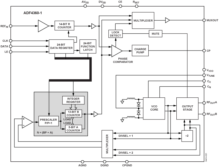
EV-ADF4360-1EB1Z
Analog Devices Inc.The ADF4360-1 is a fully integrated integer-N synthesizer andvoltage controlled oscillator (VCO). The ADF4360-1 is designed for a center frequency of 2250 MHz. In addition, there is a divide-by-2 option available, whereby the user gets an RF output of between 1025 MHz and 1225 MHz. Control of all the on-chip registers is through a simple 3-wire interface. The device operates with a power supply ranging from 3.0 V to 3.6 V and can be powered down when not in use.?
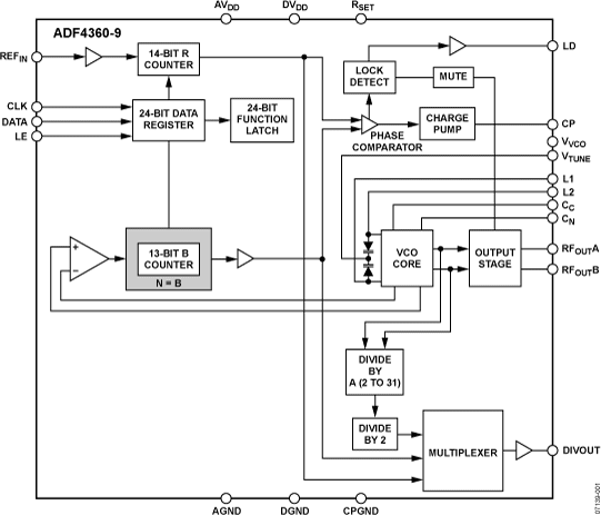
EV-ADF4360-9EB1Z
Analog Devices Inc.The ADF4360-9 is an integrated integer-N synthesizer and voltage controlled oscillator (VCO). The ADF4360-9 center frequency is set by external inductors. This allows a VCO frequency range of between65 MHz and 400 MHz. An additional divider stage allows division of the VCO signal. The CMOS level output is equivalent to the VCO signal divided by integer value between 2 and 31. This divided signal can be further divided by two if desired. Control of all the on-chip registers is through a simple 3-wire interface. The device operates with a power supply ranging from 3.0 V to 3.6 V and can be powered down when not in use.Applications System clock generation Test equipment Wireless LANs CATV equipment Data Sheet, Rev. A, 3/08

EV-ADF4377SD1Z
Analog Devices Inc.The ADF4377 is a high performance, ultralow jitter, dual output integer-N phased locked loop (PLL) with integrated voltage controlled oscillator (VCO) ideally suited for data converter and mixed signal front end (MxFE) clock applications. The high performance PLL has a figure of merit of -239 dBc/Hz, ultralow 1/f Noise and a high phase frequency detector (PFD) frequency that can achieve ultralow in-band noise and integrated jitter. The ADF4377?s fundamental VCO and output divider generate frequencies from 800 MHz to 12.8 GHz. The ADF4377 integrates all necessary power supply bypass capacitors, saving board space on compact boards.For multiple data converter and MxFE clock applications, the ADF4377 simplifies clock alignment and calibration routines required with other clock solutions, by implementing:automatic reference to output synchronization,extremely well match reference to output delays across process, voltage, and temperature, andsub-ps, jitter free reference to output delay adjustment capability.These features allow for predictable and precise multi-chip clock and SYSREF alignment. JESD204B and JESD204C subclass 1 solutions are supported by pairing the ADF4377 with an integrated circuit(IC) that distributes pairs of reference and SYSREF signals.APPLICATIONSHigh Performance Data Converter and MxFE ClockingWireless infrastructure (MC-GSM, 5G)Test and Measurement

EV-ADF4401ASD2Z
Analog Devices Inc.The ADF4401A is a fully integrated, system in package (SiP) translation loop (also known as an offset loop) module that includes a voltage controlled oscillator (VCO) and calibration phase-locked loop (PLL) circuit. Designed for highly jitter sensitive applications, this solution reduces board space and complexity compared to traditional discrete translation loop solutions designed on a printed circuit board (PCB). The time to market is significantly reduced by taking advantage of this highly integrated solution with in package circuitry and enhanced isolation that attenuates spurious components. The ADF4401A provides a frequency synthesis solution for engineers designing highly competitive systems. The ADF4401A requires an external phase detector or phase frequency detector (PFD) and an external local oscillator (LO) to form a frequency synthesis solution. The ADF4401A implements an integrated downconversion mixing stage in the feedback loop that sets the loop gain to 1 and minimizes the in band phase noise. By combining the frequency downconversion stage and low noise, integrated, wideband, VCO technology from Analog Devices, Inc., the ADF4401A offers a wideband jitter performance of 9 fs rms at 8 GHz output. The output jitter performance is largely dependent on the performance of the external offset LO. The ADF4401A module uses an internal PFD and VCO calibration circuitry to select the appropriate VCO band. The user can disable the calibration circuitry and close the loop using the external PFD. All on-chip registers are controlled via a serial port interface (SPI). APPLICATIONSInstrumentation and measurement Automated test equipment Aerospace and defense

EV-ADF5901SD2Z
Analog Devices Inc.The ADF5901 is a 24 GHz Tx monolithic microwave integrated circuit (MMIC) with an on-chip, 24 GHz VCO with PGA and dual Tx channels for radar systems. The on-chip, 24 GHz VCO generates the 24 GHz signal for the two Tx channels and the LO output. Each Tx channel contains a power control circuit. There is also an on-chip temperature sensor.Control of all the on-chip registers is through a simple 4-wire interface.The ADF5901 comes in a compact 32-lead, 5 mm ? 5 mm LFCSP package.Applications Automotive radars Industrial radars Microwave radar sensors Industrial sensors Precision instrumentation Tank level sensors Smart sensors Door opening Energy saving Commercial sensors: object detection and tracking Cars, boats, aircraft, and UAVs (drones): collision avoidance Intelligent transportation systems: intelligent traffic monitoring and control Surveillance and security

EV-ADF702X-ADAPTZ
Analog Devices Inc.The ADF7021 is a low power, highly integrated 2FSK/3FSK/4FSK transceiver. It is designed to operate in the narrowband, license-free ISM bands and licensed bands in the 80 MHz to 650 MHz and 862 MHz to 940 MHz frequency ranges. It has both Gaussian and raised cosine data filtering options to improve spectral efficiency for narrowband applications.It is suitable for circuit applications targeted at European ETSI-EN 300-220, the Japanese ARIB STD-T67, the Chinese Short Range Device regulations, and the North American FCC Part 15, Part 90, and Part 95 regulatory standards. A complete transceiver can be built using a small number of external discrete components, making the ADF7021 very suitable for price-sensitive and area-sensitive applications.The transmit section contains a voltage controlled oscillator (VCO) and a low noise fractional-N PLL with output resolution of

EV-ADGS1414DSDZ
Analog Devices Inc.The ADGS1414D contains eight independent SPST switches. A serial peripheral interface (SPI) controls the switches. The SPI has robust error detection features, such as cyclic redundancy check (CRC) error detection, invalid read and write address detection, and SCLK count error detection. It is possible to daisy-chain multiple ADGS1414D devices together. Daisy-chain mode enables the configuration of multiple devices with a minimal amount of digital lines. The route of digital signals and supplies through the ADGS1414D allows for a further increase in channel density. Integrated passive components eliminate the need for external passive components. FUNCTIONAL BLOCK DIAGRAM Figure 1. The ADGS1414D is suited to high density switching applications, such as large switching matrices and fanout applications. Each switch conducts equally well in both directions when on, and each switch has an input signal range that extends to the supplies. In the off condition, signal levels up to the supplies are blocked. Multifunction pin names may be referenced by their relevant function only.Applications? Automated test equipment Data acquisition systems Sample-and-hold systems Audio and video signal routing Communications systems Relay replacement

EV-ADUCM320QSPZ
Analog Devices Inc.The ADuCM320 is a fully integrated single package device that incorporates high performance analog peripherals together with digital peripherals controlled by an 80 MHz ARM Cortex-M3 processor and integral flash for code and data.The ADC on the ADuCM320 provides 14-bit, 1 MSPS data acquisition on up to 16 input pins that can be programmed for single-ended or differential operation. The voltage at the IDAC output pins can also be measured by the ADC, which is useful for controlling the power consumption of the current DACs. Additionally, chip temperature and supply voltages can be measured.The ADC input voltage is 0 V to VREF. A sequencer is provided, which allows a user to select a set of ADC channels to be measured in sequence without software involvement during the sequence. The sequence can optionally repeat automatically at a user selectable rate.Up to eight VDACs are provided with output ranges that are programmable to one of two voltage ranges.Four IDAC sources are provided. The output currents are programmable with ranges of 0 mA to 150 mA. A low drift band gap reference and voltage comparator completes the analog input peripheral set.The ADuCM320 can be configured so that the digital and analog outputs will retain their output voltages and currents through a watchdog or software reset sequence. Thus, a product can remain functional even while the ADuCM320 is resetting itself.The ADuCM320 has a low power ARM Cortex-M3 processor and a 32-bit RISC machine that offers up to 100 MIPS peak performance. Also integrated on chip are 2 ? 128 kB Flash/EE memory and 32 kB of SRAM. The flash comprises two separate 128 kB blocks supporting execution from one flash block and simultaneous writing/erasing of the other flash block.The ADuCM320 operates from an on-chip oscillator or a 16 MHz external crystal and a PLL at 80 MHz. This clock can optionally be divided down to reduce current consumption. Additional low power modes can be set via software. In normal operating mode, the ADuCM320 digital core consumes about 300 ?A per MHz.The device includes an MDIO interface capable of operating at up to 4 MHz. The capability to simultaneously execute from one flash block and write/erase the other flash block makes the ADuCM320 ideal for 10G, 40G, and 100G optical applications. User programming is eased by incorporating PHYADR and DEVADD hardware comparators. In addition, the nonerasable kernel code plus flags in user flash provide assistance by allowing user code to robustly switch between the two blocks of user flash code and data spaces.The ADuCM320 integrates a range of on-chip peripherals that can be configured under software control, as required in the appli-cation. These peripherals include 1 ? UART, 2 ? I2C, and 2 ? SPI serial input/output communication controllers, GPIO, 32-element programmable logic array, 3 general-purpose timers, plus a wake-up timer and system watchdog timer. A 16-bit PWM with seven output channels is also provided.GPIO pins on the device power up in high impedance input mode. In output mode, the software chooses between open-drain mode and push-pull mode. The pull-up resistors can be disabled and enabled in software. In GPIO output mode, the inputs can remain enabled to monitor the pins. The GPIO pins can also be programmed to handle digital or analog peripheral signals, in which case the pin characteristics are matched to the specific requirement.A large support ecosystem is available for the ARM Cortex-M3 processor to ease product development of the ADuCM320. Access is via the ARM serial wire debug port (SW-DP). On-chip factory firmware supports in-circuit serial download via MDIO. These features are incorporated into a low cost QuickStart development system supporting this precision analog microcontroller family. APPLICATIONS Optical networking

EV-ADUCM350-4WBCZ
Analog Devices Inc.The ADuCM350 is a configurable Impedance Converter and Potentiostat with current and voltage measurement capability for both Electrochemical sensors and Biosensors. It is a complete, coin cell powered, high precision, MCU integrated solution for portable device applications such as point-of-care diagnostics and body-worn devices for monitoring vital signs.The ADuCM350 analog front end (AFE) features a 16-bit, precision, 160 kSPS analog-to-digital converter (ADC); 0.17% precision voltage reference; 12-bit, no missing codes digital-to-analog converter (DAC); and a reconfigurable ultralow leakage switch matrix. It has 4 voltage measurement channels, up to 8 current measurement channels and an impedance measurement DFT engine. The ADuCM350 also includes an ARM Cortex-M3-based processor, memory, and all I/O connectivity to support portable meters with display, USB communication, and active sensors. The ADuCM350 is available in a 120-lead, 8 mm ? 8 mm CSP_BGA and operates from ?40?C to +85?C. To support extremely low dynamic and hibernate power management, the ADuCM350 provides a collection of power modes and features, such as dynamic and software controlled clock gating and power gating.The AFE is connected to the ARM Cortex-M3 via an advanced high performance bus (AHPB) slave interface on the advanced microcontroller bus architecture (AMBA) matrix, as well as direct memory access (DMA) and interrupt connections.APPLICATIONS Point-of-care diagnostics Body-worn devices for monitoring vital signs Amperometric, voltametric, and impedometric measurements


