EVAL-ADAU1966Z
Analog Devices Inc.The ADAU1966 is a high performance, single-chip DAC thatprovides 16 digital-to-analog converters (DACs) with differentialoutput using the Analog Devices, Inc., patented multibitsigma-delta (?-?) architecture. An SPI/I2C port is included,allowing a microcontroller to adjust volume and many otherparameters. The ADAU1966 operates from 2.5 V digital, 5 Vanalog and 3.3 V or 5 V input/output supplies. A linear regulatoris included to generate the digital supply voltage from the analogsupply voltage. The ADAU1966 is available in an 80-lead LQFPpackage.The ADAU1966 is designed for low EMI. This consideration isapparent in both the system and circuit design architectures.By using the on-board PLL to derive the internal master clockfrom an external LRCLK, the ADAU1966 can eliminate theneed for a separate high frequency master clock and can beused with or without a bit clock. The DACs are designed usingthe latest Analog Devices continuous time architectures tofurther minimize EMI. By using 2.5 V digital supplies, powerconsumption is minimized, and the digital waveforms are asmaller amplitude, further reducing emissions. Applications Automotive audio systems Home theater systems Digital audio effects processors
EVAL-ADAU1978Z
Analog Devices Inc.The ADAU1978 incorporates four high performance, analog-to-digital converters (ADCs) with 2 V rms capable ac-coupled inputs. The ADCs use a multibit sigma-delta (?-?) architecture with continuous time front end for low EMI. An I2C/serial peripheral interface (SPI) control port is included that allows a microcontroller to adjust volume and many other parameters. The ADAU1978 uses only a single 3.3 V supply. The part internally generates the required digital DVDD supply. The low power architecture reduces the power consumption. The ADAU1978 is available in a 40-lead LFCSP package. The on-chip PLL can derive the master clock from an external clock input or frame clock (sample rate clock). When fed with the frame clock, it eliminates the need for a separate high frequency master clock in the system.Note that throughout this data sheet, multifunction pins, such as SCL/CCLK, are referred to either by the entire pin name or by a single function of the pin, for example, CCLK, when only that function is relevant. APPLICATIONS Automotive audio systems Active noise cancellation system
EVAL-ADAU1979Z
Analog Devices Inc.The ADAU1979 incorporates four high performance, analog-to-digital converters (ADCs) with 4.5 V rms capable ac-coupled inputs. The ADCs use a multibit sigma-delta (?-?) architecture with continuous time front end for low EMI. An I2C/serial peripheral interface (SPI) control port is included that allows a microcontroller to adjust volume and many other parameters. The ADAU1979 uses only a single 3.3 V supply. The device internally generates the required digital DVDD supply. The low power architecture reduces the power consumption. The on-chip PLL can derive the master clock from an external clock input or frame clock (sample rate clock). When fed with the frame clock, it eliminates the need for a separate high frequency master clock in the system. The ADAU1979 is available in a 40-lead LFCSP package.Note that throughout the data sheet, multifunction pins, such as SCL/CCLK, are referred to either by the entire pin name or by a single function of the pin, for example, CCLK, when only that function is relevant.APPLICATIONS Automotive audio systems Active noise cancellation systems
EVAL-ADCM-1
Analog Devices Inc.The ADcmXL1021-1 is a complete vibration sensing system that combines high performance vibration sensing (using a microelectromechanical systems (MEMS) accelerometer) with a variety of signal processing functions to simplify the development of smart sensor nodes in condition-based monitoring (CBM) systems. The typical ultralow noise density (26 ?g/?Hz) in the MEMS accelerometers supports excellent resolution. The wide bandwidth (dc to 10 kHz within 3 dB flatness) enables tracking of key vibration signatures on many machine platforms.The signal processing includes high speed data sampling (220 kSPS), 4096 time sample record lengths, filtering, windowing, fast Fourier transform (FFT), user configurable spectral or time statistic alarms, and error flags. The serial peripheral interface (SPI) provides access to a register structure that contains the vibration data and a wide range of user configurable functions.The ADcmXL1021-1 is available in a 23.7 mm ? 27.0 mm ? 12.4 mm aluminum package with four mounting flanges to support installation with standard machine screws. This lightweight package (13 g) provides consistent mechanical coupling to the core sensors over a broad frequency range. The electrical interface is through a 14-lead connector on a 36 mm flexible cable, which enables a wide range of location and orientation options for system mating connectors.The ADcmXL1021-1 requires only a single, 3.3 V power supply and supports an operating temperature range of ?40?C to +105?C. Multifunction pin names may be referenced by their relevant function only.Applications Vibration analysis Condition-based monitoring (CbM) systems Machine health Instrumentation and diagnostics Safety shutoff sensing
EVAL-ADCMP562BRQZ
Analog Devices Inc.The ADCMP561/ADCMP562 are high speed comparators fabricated on Analog Devices, Inc., proprietary XFCB process. The devices feature a 700 ps propagation delay with less than 75 ps overdrive dispersion. Dispersion, a measure of the difference in propagation delay under differing overdrive conditions, is a particularly important characteristic of comparators. A separate programmable hysteresis pin is available on the ADCMP562.A differential input stage permits consistent propagation delay with a wide variety of signals in the common-mode range from ?2.0 Vto +3.0 V. Outputs are complementary digital signals that are fully compatible with PECL 10 K and 10 KH logic families. The outputs provide sufficient drive current to directly drive transmission lines terminated in 50 ? to VDD ? 2 V. A latch input, which is included, permits tracking, track-and-hold, or sample-and-hold modes of operation. The latch input pins contain internal pull-ups that set the latch in tracking mode when left open.The ADCMP561/ADCMP562 are specified over the industrial temperature range (?40?C to +85?C).Applications Automatic test equipment High speed instrumentation Scope and logic analyzer front ends Window comparators High speed line receivers Threshold detection Peak detection High speed triggers Patient diagnostics Disk drive read channel detection Hand-held test instruments Zero-crossing detectors Line receivers and signal restoration Clock drivers
EVAL-ADCMP572BCPZ
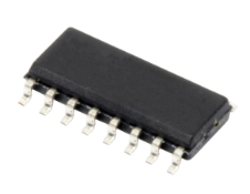
Analog Devices Inc.The ADCMP572 and ADCMP573?are ultrafast comparators fabricated on Analog Devices? proprietary XFCB3 Silicon Germanium (SiGe) bipolar process. The ADCMP572 features CML output drivers and latch inputs, and the ADCMP573 features reduced swing PECL (RSPECL) output drivers and latch inputs.Both devices offer 150 ps propagation delay and 80 ps minimum pulse width for 10 Gbps operation with 200 fs rms random jitter (RJ). Overdrive and slew rate dispersion are typically less than 15 ps.A flexible power supply scheme allows both devices to operate with a single 3.3 V positive supply and a ?0.2 V to +1.2 V input signal range or with split input/output supplies to support a wider ?0.2 V to +3.2 V input signal range and an independent range of output levels. 50 ? on-chip termination resistors are provided at both inputs with the optional capability to be left open (on an individual pin basis) for applications requiring high impedance inputs.The CML output stage is designed to directly drive 400 mV into 50 ? transmission lines terminated to between 3.3 V to 5.2 V. The RSPECL output stage is designed to drive 400 mV into 50 ? terminated to VCCO ? 2 V and is compatible with several commonly used PECL logic families. The comparator input stage offers robust protection against large input overdrive, and the outputs do not phase reverse when the valid input signal range is exceeded. High speed latch and programmable hysteresis features are also provided.The ADCMP572 and ADCMP573 are available in a 16-lead LFCSP package and have been characterized over an extended industrial temperature range of ?40?C to +125?C.APPLICATIONS Clock and data signal restoration and level shifting Automatic test equipment (ATE) High speed instrumentation Pulse spectroscopy Medical imaging and diagnostics High speed line receivers Threshold detection Peak and zero-crossing detectors High speed trigger circuitry
EVAL-ADCMP602BRMZ
Analog Devices Inc.The ADCMP600, ADCMP601, and ADCMP602 are very fast comparators fabricated on Analog Devices? proprietary XFCB2 process. These comparators are exceptionally versatile and easy to use. Features include an input range from ? 0.5 V to VCC + 0.2 V, low noise TTL-/CMOS-compatible output drivers, and latch inputs with adjustable hysteresis and/or shutdown inputs.The devices offer 5 ns propagation delay with 10 mV overdrive on 3 mA typical supply current.A flexible power supply scheme allows the devices to operate with a single +2.5 V positive supply and a ?0.5 V to +2.8 V input signal range up to a +5.5 V positive supply with a ?0.5 V to +5.8 V input signal range. Split input/output supplies with no sequencing restrictions on the ADCMP602 support a wide input signal range while still allowing independent output swing control and power savings.The TTL-/CMOS-compatible output stage is designed to drive up to 5 pF with full timing specs and to degrade in a graceful and linear fashion as additional capacitance is added. The comparator input stage offers robust protection against large input overdrive, and the outputs do not phase reverse when the valid input signal range is exceeded. High speed latch and programmable hysteresis features are also provided with a unique single-pin control option.The ADCMP600 is available in both 5-lead SC70 and SOT-23 packages, the ADCMP601 is available in a 6-lead SC70 package, and the ADCMP602 is available in 8-lead MSOP and LSCFP packages.ApplicationsHigh Speed InstrumentationClock and Data Signal RestorationLogic Level Shifting or TranslationPulse SpectroscopyHigh Speed Line ReceiversThreshold DetectionPeak and Zero-crossing DetectorsHigh Speed Trigger CircuitryPulse-width ModulatorsCurrent-/voltage-controlled OscillatorsAutomatic Test Equipment (ATE)
EVAL-ADCMP608BKSZ
Analog Devices Inc.The ADCMP608 is a fast comparator fabricated on XFCB2, an Analog Devices, Inc. proprietary process. This comparator is exceptionally versatile and easy to use. Features include an input range from VEE ? 0.2 V to VCC + 0.2 V, low noise, TTL-/CMOS-compatible output drivers, and shutdown inputs. The device offers 40 ns propagation delays driving a 15 pF load with 10 mV overdrive on 500 ?A typical supply current.A flexible power supply scheme allows the device to operate with a single +2.5 V positive supply and a ?0.2 V to + 2.7 V input signal range up to a +5.5 V positive supply with a ?0.2 V to +5.7 V input signal range.The TTL-/CMOS-compatible output stage is designed to drive up to 15 pF with full rated timing specifications and to degrade in a graceful and linear fashion as additional capacitance is added. The input stage of the comparator offers robust protection against large input overdrive, and the outputs do not phase reverse when the valid input signal range is exceeded.The ADCMP608 is available in a tiny 6-lead SC70 package with a single-ended output and a shutdown pin.APPLICATIONS High speed instrumentation Clock and data signal restoration Logic level shifting or translation High speed line receivers Threshold detection Peak and zero-crossing detectors High speed trigger circuitry Pulse-width modulators Current-/voltage-controlled oscillators
EVAL-ADE9000EBZ
Analog Devices Inc.The ADE9000 is a highly accurate, fully integrated, multiphase energy and power quality monitoring device. Superior analog performance and a digital signal processing (DSP) core enable accurate energy monitoring over a wide dynamic range. An integrated high end reference ensures low drift over temperature with a combined drift of less than ?25 ppm/?C maximum for the entire channel including a programmable gain amplifier (PGA) and an analog-to-digital converter (ADC).The ADE9000 offers complete power monitoring capability by providing total as well as fundamental measurements on rms, active, reactive, and apparent powers and energies. Advanced features such as dip and swell monitoring, frequency, phase angle, voltage total harmonic distortion (VTHD), current total harmonic distortion (ITHD), and power factor measurements enable implementation of power quality measurements. The ? cycle rms and 10 cycle rms/12 cycle rms, calculated according to IEC 61000-4-30 Class S, provide instantaneous rms measurements for real-time monitoring.The ADE9000 offers an integrated flexible waveform buffer that stores samples at a fixed data rate of 32 kSPS or 8 kSPS, or a sampling rate that varies based on line frequency to ensure 128 points per line cycle. Resampling simplifies fast Fourier transform (FFT) calculation of at least 50 harmonics in an external processor.The ADE9000 simplifies the implementation of energy and power quality monitoring systems by providing tight integration of acquisition and calculation engines. The integrated ADCs and DSP engine calculate various parameters and provide data through user accessible registers or indicate events through interrupt pins. With seven dedicated ADC channels, the ADE9000 can be used on a 3-phase system or up to three single-phase systems. It supports current transformers (CTs) or Rogowski coils for current measurements. A digital integrator eliminates a discrete integrator required for Rogowski coils.The ADE9000 absorbs most complexity in calculations for a power monitoring system. With a simple host microcontroller, the ADE9000 enables the design of standalone monitoring or protection systems, or low cost nodes uploading data into the cloud.Note that throughout this data sheet, multifunction pins, such as CF4/EVENT/DREADY, are referred to either by the entire pin name or by a single function of the pin, for example, EVENT, when only that function is relevant.Applications Energy and power monitoring Power quality monitoring Protective devices Machine health Smart power distribution units Polyphase energy meters
EVAL-ADE9153BEVKZ
Analog Devices Inc.The ADE9153B1 is a highly accurate, single-phase, energy metering IC with sensor monitoring and self-calibration. Sensor monitoring with mSure? technology allows meter health monitoring and advanced tamper detection. The monitoring feature allows the user to check the overall accuracy of the sensor and signal path to identify accuracy drifts that occur over time on the current and voltage channels, independently. Similarly, mSure offers advanced tamper detection with the ability to detect unusual changes on the sensors. mSure runs in parallel to the metering measurements, allowing uninterrupted and unaffected metrology in the ADE9153B. Self-calibration with mSure enables a meter to automatically calibrate the current and voltage channels without accurate reference meters or accurate sources when a shunt resistor is used as the current sensor. The self-calibration feature supports Class 1 and Class 2 meters.The ADE9153B includes three high performance analog-to-digital converters (ADCs), providing an 88 dB signal-to-noise ratio (SNR). The ADE9153B offers accurate measurement of line voltage and current, and calculates active, fundamental reactive, and apparent energy, as well as rms. A wide range of power quality information is included, such as dip and swell detection. Current Channel A is ideal for shunts and has a flexible gain stage providing full-scale input ranges from 62.5 mV peak down to 26.04 mV peak. Current Channel B has gain stages of 1?, 2?, and 4? for use with current transformers (CTs). A high speed, 10 MHz, serial peripheral interface (SPI) port allows access to the ADE9153B registers.1 Protected by U.S. Patents 8,350,558; 8,010,304; WO2013038176 A3; 0113507 A1; 0253102 A1; 0354266 A1; and 0154029 A1.
EVAL-ADF4007EBZ1
Analog Devices Inc.The ADF4007 is a high frequency divider/PLL synthesizer that can be used in a variety of communications applications. It can operate to 7.5 GHz on the RF side and to 120 MHz at the PFD. It consists of a low noise digital PFD (phase frequency detec-tor), a precision charge pump, and a divider/prescaler. The divider/prescaler value can be set by two external control pins to one of four values (8, 16, 32, or 64). The reference divider is permanently set to 2, allowing an external REFIN frequency of up to 240 MHz.A complete PLL (phase-locked loop) can be implemented if the synthesizer is used with an external loop filter and a VCO (voltage controlled oscillator). Its very high bandwidth means that frequency doublers can be eliminated in many high frequency systems, simplifying system architecture and reducing cost.Applications Satellite communications Broadband wireless access CATV Instrumentation Wireless LANs
EVAL-ADF4252EBZ2
Analog Devices Inc.The ADF4252 is a dual fractional-N/integer-N frequencysynthesizer that can be used to implement local oscillators (LO)in the upconversion and downconversion sections of wirelessreceivers and transmitters. Both the RF and IF synthesizersconsist of a low noise digital phase frequency detector (PFD), aprecision charge pump, and a programmable reference divider.The RF synthesizer has a ?-?-based fractional interpolator thatallows programmable fractional-N division. The IF synthesizerhas programmable integer-N counters. A complete phase-lockedloop (PLL) can be implemented if the synthesizer is used withan external loop filter and voltage controlled oscillator (VCO).Control of all the on-chip registers is via a simple 3-wire interface.The device operates with a power supply ranging from 2.7 V to3.3 V and can be powered down when not in use.Applications Base stations for mobile radio (GSM, PCS, DCS, CDMA, WCDMA) Wireless handsets (GSM, PCS, DCS, CDMA, WCDMA) Wireless LANs Communications test equipment CATV equipment
EVAL-ADF7012DBZ2
Analog Devices Inc.The ADF7012 is a low power FSK/GFSK/OOK/GOOK/ASK UHF transmitter designed for short-range devices (SRDs). The output power, output channels, deviation frequency, and modulation type are programmable by using four, 32-bit registers.The fractional-N PLL and VCO with external inductor enable the user to select any frequency in the 75 MHz to 1 GHz band. The fast lock times of the fractional-N PLL make the ADF7012 suitable in fast frequency hopping systems. The fine frequency deviations available and PLL phase noise performance facilitates narrow-band operation.There are five selectable modulation schemes: binary frequency shift keying (FSK), Gaussian frequency shift keying (GFSK), binary on-off keying (OOK), Gaussian on-off keying (GOOK), and amplitude shift keying (ASK). In the compensation register, the output can be moved in
EVAL-ADF7020-1DBZ5
Analog Devices Inc.The ADF7020-1 is a low power, highly integrated FSK/ GFSK/ ASK/ OOK/ GOOK transceiver designed for operation in thelow UHF and VHF bands. The ADF7020-1 uses an externalVCO inductor that allows users to set the operating frequencyanywhere between 135 MHz and 650 MHz. Using the divide-by-2circuit allows users to operate the device as low as 80 MHz.The typical range of the VCO is about 10% of the operatingfrequency. A complete transceiver can be built using a smallnumber of external discrete components, making the ADF7020-1 very suitable for price-sensitive and area-sensitiveapplications.The transmit section contains a VCO and low noisefractional-N PLL with output resolution of
EVAL-ADF7020DBZ1
Analog Devices Inc.The ADF7020 is a low power, low-IF transceiver designed for operation in the license-free ISM bands at 433MHz, 868MHz and 915MHz. It is suitable for circuit applications that meet either the European ETSI EN-300-220 or the North American FCC, Part 15.247 and 15.249 regulatory standards. It operates from a 2.3 V to 3.6V power supply with programmable output power from -16 to +13dBm in 0.3dBm steps. Its receiver sensitivity is -117.5dBm at 1kbits/s in FSK mode or -110.5dBm at 9.6kbits/s. Power consumption is 20mA in receive mode and 30mA in transmit mode (+10dBm output).Other features include on-chip VCO (voltage controlled oscillator), Fractional-N PLL, on-chip 7-bit ADC (analog-to-digital converter), digital received signal strength indication (RSSI), temperature sensor and a patent pending fully automatic AFC loop. This allows the ADF7020 to be used with lower tolerance crystals. Its leakage current is < 1uA in power down mode.This device is suitable for circuit applications that meet the European ETSI-300-220, the North American FCC (Part 15), or the Chinese Short Range Device regulatory standards. A complete transceiver can be built using a small number of external discrete components, making the ADF7020 very suitable for price-sensitive and area-sensitive applications. The transmitter block on the ADF7020 contains a VCO and low noise fractional-N PLL with an output resolution of
EVAL-ADF7021DBJZ
Analog Devices Inc.The ADF7021 is a low power, highly integrated 2FSK/3FSK/4FSK transceiver. It is designed to operate in the narrowband, license-free ISM bands and licensed bands in the 80 MHz to 650 MHz and 862 MHz to 940 MHz frequency ranges. It has both Gaussian and raised cosine data filtering options to improve spectral efficiency for narrowband applications.It is suitable for circuit applications targeted at European ETSI-EN 300-220, the Japanese ARIB STD-T67, the Chinese Short Range Device regulations, and the North American FCC Part 15, Part 90, and Part 95 regulatory standards. A complete transceiver can be built using a small number of external discrete components, making the ADF7021 very suitable for price-sensitive and area-sensitive applications.The transmit section contains a voltage controlled oscillator (VCO) and a low noise fractional-N PLL with output resolution of
EVAL-ADF7021-NDBEZ
Analog Devices Inc.The ADF7021-N is a high performance, low power, narrow-band transceiver based on the ADF7021. The ADF7021-N has IF filter bandwidths of 9 kHz, 13.5 kHz, and 18.5 kHz, making it ideally suited to worldwide narrowband standards and particularly those that stipulate 12.5 kHz channel separation. It is designed to operate in the narrow-band, license-free ISM bands and in the licensed bands with frequency ranges of 80 MHz to 650 MHz and 842 MHz to 916 MHz. The part has both Gaussian and raised cosine transmit data filtering options to improve spectral efficiency for narrow-band applications. It is suitable for circuit applications targeted at the Japanese ARIB STD-T67, the European ETSI EN 300 220, the Korean short range device regulations, the Chinese short range device regulations, and the North American FCC Part 15, Part 90, and Part 95 regulatory standards. A complete transceiver can be built using a small number of external discrete components, making the ADF7021-N very suitable for price-sensitive and area-sensitive applications. The range of on-chip FSK modulation and data filtering options allows users greater flexibility in their choice of modulation schemes while meeting the tight spectral efficiency requirements. The ADF7021-N also supports protocols that dynamically switch among 2FSK, 3FSK, and 4FSK to maximize communica-tion range and data throughput. The transmit section contains two voltage controlled oscillators (VCOs) and a low noise fractional-N PLL with an output resolution of The frequency-agile PLL allows the ADF7021-N to be used in frequency-hopping, spread spectrum (FHSS) systems. Both VCOs operate at twice the fundamental frequency to reduce spurious emissions and frequency pulling problems. The transmitter output power is programmable in 63 steps from ?16 dBm to +13 dBm and has an automatic power ramp control to prevent spectral splatter and help meet regulatory standards. The transceiver RF frequency, channel spacing, and modulation are programmable using a simple 3-wire interface. The device operates with a power supply range of 2.3 V to 3.6 V and can be powered down when not in use. A low IF architecture is used in the receiver (100 kHz), which minimizes power consumption and the external component count yet avoids dc offset and flicker noise at low frequencies. The IF filter has programmable bandwidths of 9 kHz, 13.5 kHz, and 18.5 kHz. The ADF7021-N supports a wide variety of pro-grammable features including Rx linearity, sensitivity, and IF bandwidth, allowing the user to trade off receiver sensitivity and selectivity against current consumption, depending on the application. The receiver also features a patent-pending automatic frequency control (AFC) loop with programmable pull-in range that allows the PLL to track out the frequency error in the incoming signal. The receiver achieves an image rejection performance of 56 dB using a patent-pending IR calibration scheme that does not require the use of an external RF source. An on-chip ADC provides readback of the integrated tempera-ture sensor, external analog input, battery voltage, and RSSI signal, which provides savings on an ADC in some applications. The temperature sensor is accurate to ?10?C over the full oper-ating temperature range of ?40?C to +85?C. This accuracy can be improved by performing a 1-point calibration at room temperature and storing the result in memory.
EVAL-ADF7021-NDBIZ
Analog Devices Inc.The ADF7021-N is a high performance, low power, narrow-band transceiver based on the ADF7021. The ADF7021-N has IF filter bandwidths of 9 kHz, 13.5 kHz, and 18.5 kHz, making it ideally suited to worldwide narrowband standards and particularly those that stipulate 12.5 kHz channel separation. It is designed to operate in the narrow-band, license-free ISM bands and in the licensed bands with frequency ranges of 80 MHz to 650 MHz and 842 MHz to 916 MHz. The part has both Gaussian and raised cosine transmit data filtering options to improve spectral efficiency for narrow-band applications. It is suitable for circuit applications targeted at the Japanese ARIB STD-T67, the European ETSI EN 300 220, the Korean short range device regulations, the Chinese short range device regulations, and the North American FCC Part 15, Part 90, and Part 95 regulatory standards. A complete transceiver can be built using a small number of external discrete components, making the ADF7021-N very suitable for price-sensitive and area-sensitive applications. The range of on-chip FSK modulation and data filtering options allows users greater flexibility in their choice of modulation schemes while meeting the tight spectral efficiency requirements. The ADF7021-N also supports protocols that dynamically switch among 2FSK, 3FSK, and 4FSK to maximize communica-tion range and data throughput. The transmit section contains two voltage controlled oscillators (VCOs) and a low noise fractional-N PLL with an output resolution of The frequency-agile PLL allows the ADF7021-N to be used in frequency-hopping, spread spectrum (FHSS) systems. Both VCOs operate at twice the fundamental frequency to reduce spurious emissions and frequency pulling problems. The transmitter output power is programmable in 63 steps from ?16 dBm to +13 dBm and has an automatic power ramp control to prevent spectral splatter and help meet regulatory standards. The transceiver RF frequency, channel spacing, and modulation are programmable using a simple 3-wire interface. The device operates with a power supply range of 2.3 V to 3.6 V and can be powered down when not in use. A low IF architecture is used in the receiver (100 kHz), which minimizes power consumption and the external component count yet avoids dc offset and flicker noise at low frequencies. The IF filter has programmable bandwidths of 9 kHz, 13.5 kHz, and 18.5 kHz. The ADF7021-N supports a wide variety of pro-grammable features including Rx linearity, sensitivity, and IF bandwidth, allowing the user to trade off receiver sensitivity and selectivity against current consumption, depending on the application. The receiver also features a patent-pending automatic frequency control (AFC) loop with programmable pull-in range that allows the PLL to track out the frequency error in the incoming signal. The receiver achieves an image rejection performance of 56 dB using a patent-pending IR calibration scheme that does not require the use of an external RF source. An on-chip ADC provides readback of the integrated tempera-ture sensor, external analog input, battery voltage, and RSSI signal, which provides savings on an ADC in some applications. The temperature sensor is accurate to ?10?C over the full oper-ating temperature range of ?40?C to +85?C. This accuracy can be improved by performing a 1-point calibration at room temperature and storing the result in memory.
EVAL-ADF7022DB1Z
Analog Devices Inc.The ADF7022 is a very low power, high performance, highlyintegrated FSK/GFSK transceiver designed for operation at thethree io-homecontrol? channels at 868.25 MHz, 868.95 MHz and 869.85 MHz in the license-free ISM band. The ADF7022 is fully compliant to ETSI-300-220, and is based on the popular ADF7020 transceiver with enhanced digital baseband features specifically designed for the io-homecontrol? standard.APPLICATIONS Home automation Process and building control


