
LTC4370CDE Demo Board | Two-Supply Diode-OR Current Sharing Controller
Analog Devices Inc.DC1741B: Demo Board for the LTC4370 Two-Supply Diode-OR Current Balancing Controller.

LTM2881-3 Low EMI Test Board (For EMI Evaluation Purposes Only, No VL & No GPIO)
Analog Devices Inc.DC1746A-A: Demo Board for LTM2881 Complete Isolated RS485/RS422 µModule Transceiver + Power.

LTM2882-5 Low EMI Test Board (For EMI Evaluation Purposes Only, No VL & No GPIO)
Analog Devices Inc.DC1747A-B: Demo Board for LTM2882 Dual Isolated RS232 µModule Transceiver + Power.
MAX5391NEVMINIQU+
Analog Devices Inc.Digital Potentiometer Development Tools Eval Kit/System MAX5386M, MAX5388, MAX5391, and MAX5393 (Dual 256-Tap,Volatile, Low-Voltage Linear Taper Digital Potentiometers)

DC338B-B
Analog Devices Inc.The LTC1563-2/LTC1563-3 are a family of extremely easy-to-use, active RC lowpass filters with rail-to-rail inputs and outputs and low DC offset suitable for systems with a resolution of up to 16 bits. The LTC1563-2, with a single resistor value, gives a unity-gain Butterworth response. The LTC1563-3, with a single resistor value, gives a unity-gain Bessel response. The proprietary architecture of these parts allows for a simple resistor calculation:R = 10k (256kHz/fC); fC = Cutoff Frequencywhere fC is the desired cutoff frequency. For many applications,this formula is all that is needed to design a filter.By simply utilizing different valued resistors, gain andother responses are achieved.The LTC1563-X features a low power mode, for the lowerfrequency applications, where the supply current is reducedby an order of magnitude and a near zero powershutdown mode.The LTC1563-Xs are available in the narrow SSOP-16package (Same footprint as an SO-8 package).Applications Discrete RC Active Filters and Modules Antialiasing Filters Smoothing or Reconstruction Filters Linear Phase Filtering for Data Communication Phase Locked Loops
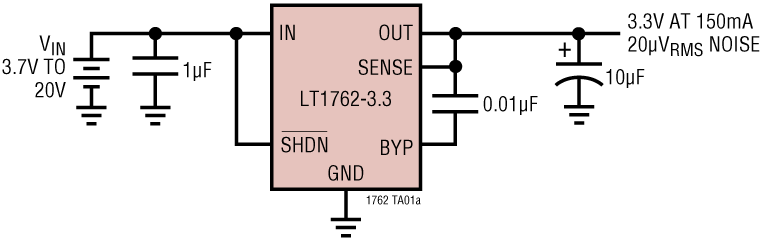
LT1762EMS8 Demo Board | Micropower Low Noise LDO Regulator, 2.3V ≤ VIN ≤ 20V, VOUT = 1.22V/2.5V/3V/3.3V/5V/Adjustable @ 150mA
Analog Devices Inc.Demonstration circuit DC339-A is a low noise micropower voltage regulator using the 150mA output current LT1762 linear regulator in an 8-lead MSOP package. The demo board has an input voltage range from 2.3V to 20V and a jumper-selectable output votlage that can be set to 1.22V, 2.5V, 3.0V, 3.3V, 5V or a user-defined value. The LT1762's low 20µVRMS (10Hz to 100kHz bandwidth) output noise and low 30µA quiescent current make the device ideal for voltage-controlled oscillators, RF power supplies and local regulators in larger systems.

DC342A-A
Analog Devices Inc.The LTC1911 is a switched capacitor step-down DC/DC converter that produces a 1.5V or 1.8V regulated output from a 2.7V to 5.5V input. The part uses switched capacitor fractional conversion to achieve high efficiency over the entire input range. No inductors are required. Internal circuitry controls the step-down conversion ratio to optimize efficiency as the input voltage and load conditions vary. Typical efficiency is over 25% higher than that of a linear regulator.A unique constant frequency architecture provides a low noise regulated output as well as lower input noise than conventional charge pump regulators. High frequency operation (fOSC = 1.5MHz) simplifies output filtering to further reduce conducted noise. To optimize efficiency,the part enters Burst Mode? operation under light load conditions.Low operating current (180?A with no load, 10?A in shutdown) and low external parts count (two 1?F flying capacitors and two 10?F bypass capacitors) make the LTC1911 ideally suited for space constrained battery powered applications. The part is short-circuit and over temperature protected, and is available in an 8-pin MSOP package.Applications Handheld Computers Cellular Phones Smart Card Readers Portable Electronic Equipment Handheld Medical Instruments Low Power DSP Supplies

DC354A
Analog Devices Inc.The LT1768 is designed to control single or multiple cold cathode fluorescent lamp (CCFL) displays. A unique Multimode Dimming scheme* combines both linear and PWM control functions to maximize lamp life, efficiency, and dimming range. Accurate maximum and minimum lamp currents can be easily set. The LT1768 can detect and protect against lamp failures and overvoltage start-up conditions. It is designed to provide maximum flexibility with a minimum number of external components.The LT1768 is a current mode PWM controller with a 1.5A MOSFET driver for high power applications. It contains a 350kHz oscillator, 5V reference, and a current sense comparator with a 100mV threshold. It operates from an 8V to 24V input voltage. The LT1768 also has undervoltage lockout, thermal limit, and a shutdown pin that reduces supply current to 65?A. It is available in a small 16-lead SSOP package.Applications Desktop Flat Panel Displays Multiple Lamp Displays Notebook LCD Displays Point of Sale Terminal Displays

LTC3200EMS8 Demo Board | Regulated Charge Pump White LED Driver, 2.7V ≤ VIN ≤ 4.5V, IOUT Drives 6 Parallel LEDs
Analog Devices Inc.Demonstration Circuit 366A is a low noise constant frequency regulated charge pump featuring the 100mA output current LTC3200. The demo board accepts a 2.7V to 4.5V input voltage and drives six white LEDs in parallel, resulting in 16.6mA per LED. Ballast resistors are employed to provide more uniform light intensity fromr the paralleled LEDs.

DC367A
Analog Devices Inc.The LT1963 series are low dropout regulators optimized for fast transient response. The devices are capable of supplying 1.5A of output current with a dropout voltage of 340mV. Operating quiescent current is 1mA, dropping to

LTC3714EG | Intel's Notebook Processor Power Supply, 7.5V to 24V Input, 0.6V to 1.75VOUT @ 20A
Analog Devices Inc.DC371A: Demo Board for the LTC3714 Intel Compatible, Wide Operating Range, Step-Down Controller with Internal Op Amp.

LTC3778EF | High Efficiency Notebook CPU Power Supply, Ultra Low Voltage Tualatin, VIN = 7.5V - 24V, VCORE = 1.1V/13Amax + VID
Analog Devices Inc.DC389A-C: Demo Board for LTC3778 Wide Operating Range, No RSENSE Step-Down Controller.

LTC1628CUH Demo Board | Dual Output, 5V to 24VIN, 5VOUT1 @ 4A, 3.3VOUT2 @ 5A
Analog Devices Inc.Demonstration circuit 392 is a dual output, step-down, synchronous buck converter featuring either the 150kHz to 300kHz LTC1628EUH controller (DC392A-A), the 250kHz to 550kHz LTC3728EUH (DC392A-B) or 250kHz to 550kHz LTC3728LUH (DC392A-C). It operates with an input voltage range of 7V to 24V and provides 3.3V @ 5A and 5V @ 4A at its output.
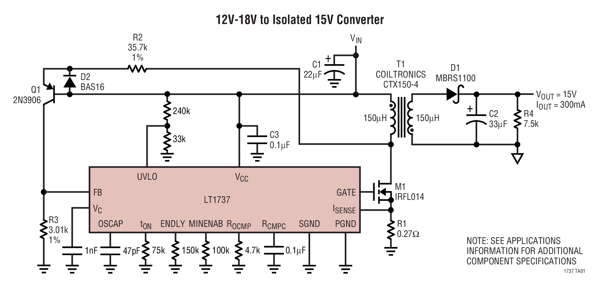
DC418A
Analog Devices Inc.The LT1737 is a monolithic switching regulator controller specifically designed for the isolated flyback topology. It drives the gate of an external MOSFET and is generally powered from a DC supply voltage. Output voltage feedback information may be supplied by a variety of methods including a third transformer winding, the primary winding or even direct DC feedback (see Applications Information). Its gate drive capability, coupled with a suitable external MOSFET and other power path components, can deliver load power up to tens of Watts.The LT1737 has a number of features not found on other isolated flyback controller ICs presently available. By utilizing current mode switching techniques, it provides excellent AC and DC line regulation. Its unique control circuitry can maintain regulation well into discontinuous mode in most applications. Optional load compensation circuitry allows for improved load regulation. An optional undervoltage lockout pin halts operation when the application input voltage is too low. An optional external capacitor implements a soft-start function.Applications Isolated Flyback Switching Regulators Medical Instruments Instrumentation Power Supplies

LTC3440EMS Demo Board (MSOP)| 1MHz, Synchronous Buck-Boost, VIN = 2.5V to 5.5V, VOUT = 3.3V @ 0.6A
Analog Devices Inc.Demonstration Circuit 425B is a constant-frequency synchronous Buck-Boost converter using the LTC3440. The input range is from 2.5V to 5.5V, making it ideal for single-cell lithium-ion or three-cell NiCd/NiMH battery applications. For 2.7V minimum input voltage, this converter can provide up to 600mA load current. The output voltage is set at 3.3V. A different output voltage in the range of 2.5V to 5.5V can be obtained by changing one of the feedback resistors.

LTC3731CG | 3-Phase, VIN = 9V to 14V, VOUT = 2.5V/1.8V @ 60A
Analog Devices Inc.Demonstration circuit 438 is a triple phase, single output synchronous buck converter featuring the LTC3731CG. This circuit can be used for desktop computers and servers, notebook computers and other high output current DC/DC converters. The output voltage can be configured for either 2.5V or 1.8V and the maximum load current is 60A. The input voltage range of DC438 is 9V to 14V.

LTC3728EUH | 2-Phase Dual Output Power Supply, VIN = 5V - 14V, VOUT1 = 2.5V @ 13A, VOUT2 = 1.8V @ 13A
Analog Devices Inc.Demonstration circuit 447 is a step-down converter featuring the LTC3728EUH regulator. The PolyPhase® dual output controller LTC3728EUH drives two high current synchronous buck converters. Input is 5V–14V, output 1 is 2.5V with loads up to 13A and output 2 is 1.8V with loads up to 13A. For applications with input voltage less than 5V, DC447 includes a circuit footprint on the bottom side to provide a 5V bias power supply.

LTC3717EGN | DDR, HSTL, STTL Termination Power Supply, 5V-20VIN, VREF/2 @ 12A
Analog Devices Inc.DC450A: Demo Board for LTC3717 Wide Operating Range, No RSENSE Step-Down Controller for DDR/QDR Memory Termination.


