ADRV9008-2W/PCBZ
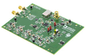
Analog Devices Inc.The ADRV9008-2 is a highly integrated, RF agile transmit subsystem offering dual channel transmitters, observation path receiver, integrated synthesizers, and digital signal processing functions. The IC delivers a versatile combination of high performance and low power consumption demanded by 2G, 3G and 4G macro-cell base stations, and active antenna, applications.The transmitters use an innovative direct conversion modulator that achieves multi-carrier macro-base-station quality performance and very low power. In 3G/4G mode, the maximum large-signal bandwidth is 200MHz. In MC-GSM mode, which has higher in-band SFDR, the maximum large-signal bandwidth is 75MHz.The observation path consists of a wide bandwidth direct-conversion receiver with state-of-the-art dynamic range. The complete receive subsystem includes dc offset correction, quadrature correction, and digital filtering thus eliminating the need for these functions in the digital baseband. Several auxiliary functions such as ADCs, DACs, and GPIOs for PA and RF-front-end control are also integrated. The fully integrated phase locked loops (PLLs) provide high performance, low power fractional-N RF frequency synthesis for the transmitter and receiver sections. An additional synthesizer is used to generate the clocks needed for the converters, digital circuits, and the serial interface. Special precautions have been taken to provide the isolation demanded in high performance base station applications. All VCO and loop filter components are integrated.The high-speed JESD204B interface supports up to 12.288 Gbps lane rates resulting in two lanes per transmitter in the widest bandwidth mode and two lanes for the observation path receiver in the widest bandwidth mode. The core of the ADRV9008-2 can be powered directly from 1.3 V and 1.8 V regulators and is controlled via a standard 4 wire serial port. Comprehensive power-down modes are included to minimize power consumption in normal use. The ADRV9008-2 is packaged in a 12mm ? 12 mm, 196-ball chip scale ball grid array (CSP_BGA).
ADRV9009-W/PCBZ
Analog Devices Inc.The ADRV9009 is a highly integrated, radio frequency (RF), agile transceiver offering dual transmitters and receivers, integrated synthesizers, and digital signal processing functions. The IC delivers a versatile combination of high performance and low power consumption demanded by 3G, 4G, and 5G macro cell time division duplex (TDD) base station applications.The receive path consists of two independent, wide bandwidth, direct conversion receivers with state-of-the-art dynamic range. The device also supports a wide bandwidth, time shared observation path receiver (ORx) for use in TDD applications. The complete receive subsystem includes automatic and manual attenuation control, dc offset correction, quadrature error correction (QEC), and digital filtering, thus eliminating the need?for these functions in the digital baseband. Several auxiliary functions, such as analog-to-digital converters (ADCs), digital-to-analog converters (DACs), and general-purpose inputs/outputs (GPIOs) for the power amplifier (PA), and RF front-end control are also integrated.In addition to automatic gain control (AGC), the ADRV9009 also features flexible external gain control modes, allowing significant flexibility in setting system level gain dynamically.The received signals are digitized with a set of four high dynamic range, continuous time ?-? ADCs that provide inherent antialiasing. The combination of the direct conversion architecture, which does not suffer from out of band image mixing, and the lack of aliasing, relaxes the requirements of the RF filters when compared to traditional intermediate frequency (IF) receivers.The transmitters use an innovative direct conversion modulator that achieves high modulation accuracy with exceptionally low noise.The observation receiver path consists of a wide bandwidth, direct conversion receiver with state-of-the-art dynamic range.The fully integrated phase-locked loop (PLL) provides high performance, low power, fractional-N RF frequency synthesis for the transmitter (Tx) and receiver (Rx) signal paths. An additional synthesizer generates the clocks needed for the converters, digital circuits, and the serial interface. A multichip synchronization mechanism synchronizes the phase of the RF local oscillator (LO) and baseband clocks between multiple ADRV9009 chips. Precautions are taken to provide the isolation required in high performance base station applications. All voltage controlled oscillators (VCOs) and loop filter components are integrated.The high speed JESD204B interface supports up to 12.288 Gbps lane rates, resulting in two lanes per transmitter and a single lane per receiver in the widest bandwidth mode. The interface also supports interleaved mode for lower bandwidths, thus reducing the total number of high speed data interface lanes to one. Both fixed and floating point data formats are supported. The floating point format allows internal AGC to be invisible to the demodulator device.The core of the ADRV9009 can be powered directly from 1.3 V regulators and 1.8 V regulators, and is controlled via a standard 4-wire serial port. Comprehensive power-down modes are included to minimize power consumption in normal use. The ADRV9009 is packaged in a 12 mm ? 12 mm, 196-ball chip scale ball grid array (CSP_BGA).Applications 3G, 4G, and 5G TDD macrocell base stations TDD active antenna systems Massive multiple input, multiple output (MIMO) Phased array radar Electronic warfare Military communications Portable test equipment
ADRV9029-LB/PCBZ
Analog Devices Inc.The ADRV9029 is a highly integrated, radio frequency (RF) agile transceiver offering four independently controlled transmitters, dedicated observation receiver inputs for monitoring each transmitter channel, four independently controlled receivers, integrated synthesizers, and digital signal processing functions providing a complete transceiver solution. The device provides the performance demanded by cellular infrastructure applications, such as small cell base station radios, macro 3G/4G/5G systems, and massive multiple in/multiple out (MIMO) base stations.The receiver subsystem consists of four independent, wide bandwidth, direct conversion receivers with wide dynamic range. The four independent transmitters use a direct conversion modulator resulting in low noise operation with low power consumption. The device also includes two wide bandwidth, time shared, observation path receivers with two inputs each for monitoring transmitter outputs.The complete transceiver subsystem includes automatic and manual attenuation control, dc offset correction, quadrature error correction (QEC), and digital filtering, eliminating the need for these functions in the digital baseband. Other auxiliary functions such as analog-to-digital converters (ADCs), digital-to-analog converters (DACs), and general-purpose input/ outputs (GPIOs) that provide an array of digital control options are also integrated.To achieve a high level of RF performance, the transceiver includes five fully integrated phase-locked loops (PLLs). Two PLLs provide low noise and low power fractional-N RF synthesis for the transmitter and receiver signal paths. A third fully integrated PLL supports an independent local oscillator (LO) mode for the observation receiver. The fourth PLL generates the clocks needed for the converters and digital circuits, and a fifth PLL provides the clock for the serial data interface.A multichip synchronization mechanism synchronizes the phase of all LOs and baseband clocks between multiple ADRV9029 chips. All voltage controlled oscillators (VCOs) and loop filter components are integrated and adjustable through the digital control interface.This device contains a fully integrated, low power digital predistortion (DPD) adaptation engine for use in power amplifier linearization. DPD enables use of high efficiency power amplifiers, reducing the power consumption of base station radios while also reducing the number of SERDES lanes necessary to interface with baseband processors.The low power crest factor reduction (CFR) engine of the ADRV9029 reduces the peak to average ratio (PAR) of the input signal, enabling higher efficiency transmit line ups while reducing the processing load on baseband processors.The serial data interface consists of four serializer lanes and four deserializer lanes. The interface supports both the JESD204B and JESD204C standards, operating at data rates up to 24.33 Gbps. The interface also supports interleaved mode for lower bandwidths, thus reducing the number of high speed data interface lanes to one. Both fixed and floating-point data formats are supported. The floating-point format allows internal automatic gain control (AGC) to be invisible to the demodulator device.The ADRV9029 is powered directly from 1.0 V, 1.3 V, and 1.8 V regulators and is controlled via a standard serial peripheral interface (SPI) serial port. Comprehensive power-down modes are included to minimize power consumption in normal use. The ADRV9029 is packaged in a 14 mm ? 14 mm, 289-ball chip scale ball grid array (CSP_BGA).APPLICATIONS3G/4G/5G TDD and FDD massive MIMO, macro and small cell base stations
ADRV9029-MB/PCBZ
Analog Devices Inc.The ADRV9029 is a highly integrated, radio frequency (RF) agile transceiver offering four independently controlled transmitters, dedicated observation receiver inputs for monitoring each transmitter channel, four independently controlled receivers, integrated synthesizers, and digital signal processing functions providing a complete transceiver solution. The device provides the performance demanded by cellular infrastructure applications, such as small cell base station radios, macro 3G/4G/5G systems, and massive multiple in/multiple out (MIMO) base stations.The receiver subsystem consists of four independent, wide bandwidth, direct conversion receivers with wide dynamic range. The four independent transmitters use a direct conversion modulator resulting in low noise operation with low power consumption. The device also includes two wide bandwidth, time shared, observation path receivers with two inputs each for monitoring transmitter outputs.The complete transceiver subsystem includes automatic and manual attenuation control, dc offset correction, quadrature error correction (QEC), and digital filtering, eliminating the need for these functions in the digital baseband. Other auxiliary functions such as analog-to-digital converters (ADCs), digital-to-analog converters (DACs), and general-purpose input/ outputs (GPIOs) that provide an array of digital control options are also integrated.To achieve a high level of RF performance, the transceiver includes five fully integrated phase-locked loops (PLLs). Two PLLs provide low noise and low power fractional-N RF synthesis for the transmitter and receiver signal paths. A third fully integrated PLL supports an independent local oscillator (LO) mode for the observation receiver. The fourth PLL generates the clocks needed for the converters and digital circuits, and a fifth PLL provides the clock for the serial data interface.A multichip synchronization mechanism synchronizes the phase of all LOs and baseband clocks between multiple ADRV9029 chips. All voltage controlled oscillators (VCOs) and loop filter components are integrated and adjustable through the digital control interface.This device contains a fully integrated, low power digital predistortion (DPD) adaptation engine for use in power amplifier linearization. DPD enables use of high efficiency power amplifiers, reducing the power consumption of base station radios while also reducing the number of SERDES lanes necessary to interface with baseband processors.The low power crest factor reduction (CFR) engine of the ADRV9029 reduces the peak to average ratio (PAR) of the input signal, enabling higher efficiency transmit line ups while reducing the processing load on baseband processors.The serial data interface consists of four serializer lanes and four deserializer lanes. The interface supports both the JESD204B and JESD204C standards, operating at data rates up to 24.33 Gbps. The interface also supports interleaved mode for lower bandwidths, thus reducing the number of high speed data interface lanes to one. Both fixed and floating-point data formats are supported. The floating-point format allows internal automatic gain control (AGC) to be invisible to the demodulator device.The ADRV9029 is powered directly from 1.0 V, 1.3 V, and 1.8 V regulators and is controlled via a standard serial peripheral interface (SPI) serial port. Comprehensive power-down modes are included to minimize power consumption in normal use. The ADRV9029 is packaged in a 14 mm ? 14 mm, 289-ball chip scale ball grid array (CSP_BGA).APPLICATIONS3G/4G/5G TDD and FDD massive MIMO, macro and small cell base stations
ADRV9371-W/PCBZ
Analog Devices Inc.The AD9371 is a highly integrated, wideband RF transceiveroffering dual channel transmitters and receivers, integrated synthesizers, and digital signal processing functions. The ICdelivers a versatile combination of high performance and low power consumption required by 3G/4G micro and macro BTSequipment in both FDD and TDD applications. The AD9371operates from 300 MHz to 6000 MHz, covering most of the licensed and unlicensed cellular bands. The IC supports receiver bandwidths up to 100 MHz. It also supports observation receiver and transmit synthesis bandwidths up to 250 MHz to accommodate digital correction algorithms.The transceiver consists of wideband direct conversion signalpaths with state-of-the-art noise figure and linearity. Each complete receiver and transmitter subsystem includes dc offset correction, quadrature error correction (QEC), and programmable digitalfilters, eliminating the need for these functions in the digitalbaseband. Several auxiliary functions such as an auxiliary analog-to-digital converter (ADC), auxiliary digital-to-analog converters (DACs), and general-purpose input/outputs (GPIOs) are integratedto provide additional monitoring and control capability.An observation receiver channel with two inputs is included to monitor each transmitter output and implement interference mitigation and calibration applications. This channel also connects to three sniffer receiver inputs that can monitor radio activity in different bands.The high speed JESD204B interface supports lane rates up to 6144 Mbps. Four lanes are dedicated to the transmitters and four lanes are dedicated to the receiver and observation receiver channels.The fully integrated phase-locked loops (PLLs) provide high performance, low power fractional-N frequency synthesis forthe transmitter, the receiver, the observation receiver, and theclock sections. Careful design and layout techniques provide theisolation demanded in high performance base station applications.All voltage controlled oscillator (VCO) and loop filter components are integrated to minimize the external component count. A 1.3 V supply is required to power the core of the AD9371, anda standard 4-wire serial port controls it. Other voltage supplies provide proper digital interface levels and optimize transmitterand auxiliary converter performance. The AD9371 is packaged in a12 mm ? 12 mm, 196-ball chip scale ball grid array (CSP_BGA).Applications 3G/4G micro and macro base stations (BTS) 3G/4G multicarrier picocells? FDD and TDD active antenna systems? Microwave, nonline of sight (NLOS) backhaul systems
ADV3205-EVALZ
Analog Devices Inc.The ADV3205 is a fully buffered crosspoint switch matrix that operates on ?5 V, making it ideal for video applications. It offers a ?3 dB signal bandwidth of 60 MHz and channel switch times of less than 60 ns with 0.1% settling. The ADV3205 has excellent crosstalk performance, and ground/power pins surround all inputs and outputs to provide extra shielding required for the most demanding applications. The differential gain and differential phase of better than 0.1% and 0.1?, respectively, along with 0.1 dB flatness out to 10 MHz, make the ADV3205 an excellent choice for many video applications.The ADV3205 includes 16 independent output buffers that can be placed into a disabled state for paralleling crosspoint outputs. The ADV3205 has a gain of +2 and operates on voltage supplies of ?5 V while consuming only 34 mA of current. Channel switching is performed via a serial digital control (which can accommodate daisy-chaining of several devices) or via a parallel control, allowing updating of an individual output without reprogramming the entire array.?The ADV3205 is packaged in a 100-lead LQFP and is available over the commercial temperature range of 0?C to 70?C.?ApplicationsCCTV surveillanceVideo routers (NTSC, PAL, S-Video, SECAM)Video conferencing
ADV3220-EVALZ
Analog Devices Inc.The ADV3219 and ADV3220 are high speed, high slew rate,buffered, 2:1 analog multiplexers. They offer a ?3 dB signalbandwidth greater than 800 MHz and channel switch times ofless than 20 ns with 1% settling. With ?82 dB of crosstalk and?88 dB isolation (at 5 MHz), the ADV3219 and ADV3220 areuseful in many high speed applications. The differential gain ofless than 0.02% and the differential phase of less than 0.02?,together with 0.1 dB flatness beyond 100 MHz while driving a75 ? back terminated load, make the ADV3219 and ADV3220ideal for all types of signal switching. The ADV3219/ADV3220 include an output buffer that can beplaced into a high impedance state to allow multiple outputs tobe connected together for cascading stages without the off channelsloading the output bus. The ADV3219 has a gain of +1, and theADV3220 has a gain of +2; they both operate on ?5 V supplieswhile consuming less than 7.5 mA of idle current.The ADV3219/ADV3220 are available in the 8-lead LFCSPpackage over the extended industrial temperature range of?40?C to +85?C. Applications Routing of high speed signals including ??Video (NTSC, PAL, S, SECAM, YUV, and RGB) ??Compressed video (MPEG, wavelet) ??3-level digital video (HDB3) Data communications Telecommunications
ADV3227-EVALZ
Analog Devices Inc.The ADV3226/ADV3227 are high speed 16 ? 16 analog crosspoint switch matrices. They offer a ?3 dB signal bandwidth greater than 750 MHz and channel switch times of less than 20 ns with 1% settling.The ADV3226/ADV3227 include 16 independent output buffers that can be placed into a high impedance state for paralleling crosspoint outputs to prevent off channels from loading the output bus. The ADV3226 has a gain of +1 and the ADV3227 has a gain of +2. They both operate on voltage supplies of ?5 V while consuming only 118 mA (ADV3226) and 133 mA (ADV3227) of idle current. Channel switching is performed via a serial digital control that can accommodate daisy chaining of several devices or via a parallel control to allow updating of an individual output without reprogramming the entire array.The ADV3226/ADV3227 are available in the 100-lead LFCSP package over the extended industrial temperature range of ?40?C to +85?C.Applications Routing of high speed signals including ? ? Video (NTSC, PAL, S, SECAM, YUV, RGB) ? ? Compressed video (MPEG, wavelet) ? ? 3-level digital video (HDB3) Data communications Telecommunications
ADV3228-EVALZ
Analog Devices Inc.The ADV3228/ADV3229 are high speed 8 ? 8 analog crosspoint switch matrices. They offer a ?3 dB large signal bandwidth of 750 MHz (ADV3228) and a slew rate of 2500 V/?s.The ADV3228/ADV3229 include eight independent output buffers that can be placed into a high impedance state for paralleling crosspoint outputs to prevent off channels from loading the output bus. The ADV3228 has a gain of +1, the ADV3229 has a gain of +2, and they both operate on voltage supplies of ?5 V. Channel switching is performed via a serial digital control that can accommodate daisy chaining of several devices or via a parallel control to allow updating of an individual output without reprogramming the entire array.The ADV3228/ADV3229 are available in the 72-lead LFCSP package over the extended industrial temperature range of ?40?C to +85?C.Applications Routing of high speed signals including: ? ? ? Video (NTSC, PAL, S, SECAM, YUV, RGB) ? ? ? Compressed video (MPEG, wavelet) ? ? ? 3-level digital video (HDB3) Data communications Telecommunications
ADXL213EB
Analog Devices Inc.The ADXL213 is a low cost, low power, complete dual axis accelerometer with signal conditioned, duty cycle modulated outputs, all on a single monolithic IC. The ADXL213 measures acceleration with a full-scale range of ?1.2 g (typical). The ADXL213 can measure both dynamic acceleration (e.g., vibration) and static acceleration (e.g., gravity).The outputs are digital signals whose duty cycles (ratio of pulse width to period) are proportional to acceleration (30%/g). The duty cycle outputs can be directly measured by a microcontroller without an A/D converter or glue logic.Innovative design techniques are used to ensure high zero g bias stability (typically better than 0.25 mg/?C), as well as tight sensitivity stability (typically better than 50 ppm/?C).The typical noise floor is 160 ?g/?, allowing signals below 1 mg (0.06? of inclination) to be resolved in tilt sensing applications using narrow bandwidths (The user selects the bandwidth of the accelerometer usingcapacitors CX and CYM at the XFILT and YFILT pins. Bandwidths of0.5 Hz to 250 Hz may be selected to suit the application.The ADXL213 is available in a 5mm x 5mm x 2mm, 8-pad hermetic LCC package.ApplicationsAutomotive tilt alarmData projectorsNavigationPlatform stabilization/levelingAlarms and motion detectorsHigh accuracy, 2-axis tilt sensing
Amplifier Mezzanine Card for ADA4500-2
Analog Devices Inc.The Analog Devices, Inc., amplifier mezzanine card (AMC) analog-to-digital converter (ADC) driver evaluates the performance of amplifiers in 8-lead, single and dual SOIC, 6-lead single SOT23, 8-lead dual MSOP, and 16-lead LFCSP
packages. This add on board can be inserted on ADC evaluation boards using its 7-pin header. Figure 1 shows the AMC mounted on an Analog Devices, Inc., ADC evaluation board.
The AMC can support any of Analog Devices operational amplifiers and ADC drivers in different packages. The user can configure the ADC driver as a Sallen-Key low-pass, high-pass, or band-pass filter, as a multiple feedback low-pass, high-pass, or band-pass filter, or as an inverting and noninverting operational amplifier. The user can also configure the AMC to drive a single-ended, fully differential, or a single-ended signal to a differential ADC.
Optimized power and ground planes ensure low noise and high speed operation. Component placement and power supply bypassing are optimized for maximum circuit flexibility and performance. The AMC evaluation board accepts 0402 or 0603 surface mount technology (SMT) components, 1206 bypass capacitors, and 2.54 mm headers.
All components are placed on the primary side. No components are placed on the secondary side.
Amplifier Mezzanine Card for ADA4805-2
Analog Devices Inc.The Analog Devices, Inc., amplifier mezzanine card (AMC) analog-to-digital converter (ADC) driver evaluates the performance of amplifiers in 8-lead, single and dual SOIC, 6-lead single SOT23, 8-lead dual MSOP, and 16-lead LFCSP
packages. This add on board can be inserted on ADC evaluation boards using its 7-pin header. Figure 1 shows the AMC mounted on an Analog Devices, Inc., ADC evaluation board.
The AMC can support any of Analog Devices operational amplifiers and ADC drivers in different packages. The user can configure the ADC driver as a Sallen-Key low-pass, high-pass, or band-pass filter, as a multiple feedback low-pass, high-pass, or band-pass filter, or as an inverting and noninverting operational amplifier. The user can also configure the AMC to drive a single-ended, fully differential, or a single-ended signal to a differential ADC.
Optimized power and ground planes ensure low noise and high speed operation. Component placement and power supply bypassing are optimized for maximum circuit flexibility and performance. The AMC evaluation board accepts 0402 or 0603 surface mount technology (SMT) components, 1206 bypass capacitors, and 2.54 mm headers.
All components are placed on the primary side. No components are placed on the secondary side.
Amplifier Mezzanine Card for ADA4807-2
Analog Devices Inc.The Analog Devices, Inc., amplifier mezzanine card (AMC) analog-to-digital converter (ADC) driver evaluates the performance of amplifiers in 8-lead, single and dual SOIC, 6-lead single SOT23, 8-lead dual MSOP, and 16-lead LFCSP
packages. This add on board can be inserted on ADC evaluation boards using its 7-pin header. Figure 1 shows the AMC mounted on an Analog Devices, Inc., ADC evaluation board.
The AMC can support any of Analog Devices operational amplifiers and ADC drivers in different packages. The user can configure the ADC driver as a Sallen-Key low-pass, high-pass, or band-pass filter, as a multiple feedback low-pass, high-pass, or band-pass filter, or as an inverting and noninverting operational amplifier. The user can also configure the AMC to drive a single-ended, fully differential, or a single-ended signal to a differential ADC.
Optimized power and ground planes ensure low noise and high speed operation. Component placement and power supply bypassing are optimized for maximum circuit flexibility and performance. The AMC evaluation board accepts 0402 or 0603 surface mount technology (SMT) components, 1206 bypass capacitors, and 2.54 mm headers.
All components are placed on the primary side. No components are placed on the secondary side.
Amplifier Mezzanine Card for ADA4841-2
Analog Devices Inc.The Analog Devices, Inc., amplifier mezzanine card (AMC) analog-to-digital converter (ADC) driver evaluates the performance of amplifiers in 8-lead, single and dual SOIC, 6-lead single SOT23, 8-lead dual MSOP, and 16-lead LFCSP
packages. This add on board can be inserted on ADC evaluation boards using its 7-pin header. Figure 1 shows the AMC mounted on an Analog Devices, Inc., ADC evaluation board.
The AMC can support any of Analog Devices operational amplifiers and ADC drivers in different packages. The user can configure the ADC driver as a Sallen-Key low-pass, high-pass, or band-pass filter, as a multiple feedback low-pass, high-pass, or band-pass filter, or as an inverting and noninverting operational amplifier. The user can also configure the AMC to drive a single-ended, fully differential, or a single-ended signal to a differential ADC.
Optimized power and ground planes ensure low noise and high speed operation. Component placement and power supply bypassing are optimized for maximum circuit flexibility and performance. The AMC evaluation board accepts 0402 or 0603 surface mount technology (SMT) components, 1206 bypass capacitors, and 2.54 mm headers.
All components are placed on the primary side. No components are placed on the secondary side.
Amplifier Mezzanine Card for ADA4896-2
Analog Devices Inc.The Analog Devices, Inc., amplifier mezzanine card (AMC) analog-to-digital converter (ADC) driver evaluates the performance of amplifiers in 8-lead, single and dual SOIC, 6-lead single SOT23, 8-lead dual MSOP, and 16-lead LFCSP
packages. This add on board can be inserted on ADC evaluation boards using its 7-pin header. Figure 1 shows the AMC mounted on an Analog Devices, Inc., ADC evaluation board.
The AMC can support any of Analog Devices operational amplifiers and ADC drivers in different packages. The user can configure the ADC driver as a Sallen-Key low-pass, high-pass, or band-pass filter, as a multiple feedback low-pass, high-pass, or band-pass filter, or as an inverting and noninverting operational amplifier. The user can also configure the AMC to drive a single-ended, fully differential, or a single-ended signal to a differential ADC.
Optimized power and ground planes ensure low noise and high speed operation. Component placement and power supply bypassing are optimized for maximum circuit flexibility and performance. The AMC evaluation board accepts 0402 or 0603 surface mount technology (SMT) components, 1206 bypass capacitors, and 2.54 mm headers.
All components are placed on the primary side. No components are placed on the secondary side.
AMC-ADA4945-1EBZ
Analog Devices Inc.The ADA4945-1 is a low noise, low distortion, fully differential amplifier with two selectable power modes. The device operates over a broad power supply range of 3 V to 10 V. The low dc offset, dc offset drift, and excellent dynamic performance of the ADA4945-1 makes it well suited for a variety of data acquisition and signal processing applications. The device is an ideal choice for driving high resolution, high performance successive approximation register (SAR) and ?-? analog-to-digital converters (ADCs) on 4 mA of quiescent current (full power mode). The device can also be selected to operate on 1.4 mA of quiescent current (low power mode) to scale the power consumption to the desired performance necessary for an ADC drive application. The adjustable common-mode voltage allows the ADA4945-1 to match the input common-mode voltage of multiple ADCs. The internal common-mode feedback loop provides exceptional output balance, as well as suppression of even order harmonic distortion products.With the ADA4945-1, differential gain configurations are achieved with a simple external feedback network of four resistors determining the closed-loop gain of the amplifier. The ADA4945-1 is fabricated using Analog Devices, Inc., proprietary, silicon germanium (SiGe), complementary bipolar process, enabling the device to achieve low levels of distortion with an input voltage noise of only 1.8 nV/?Hz (full power mode).The ADA4945-1 is available in a RoHS-complaint, 3 mm ? 3 mm, 16-lead LFCSP. The ADA4945-1 is specified to operate from ?40?C to +125?C.Applications Low power ?-?, PulSAR?, and SAR ADC drivers Single-ended to differential converters Differential buffers Medical imaging Process control Portable electronics
DC082B
Analog Devices Inc.The LT1182/LT1183 are dual current mode switching regulators that provide the control function for Cold Cathode Fluorescent Lighting (CCFL) and Liquid Crystal Display (LCD) Contrast. The LT1184/LT1184F provide only the CCFL function. The ICs include high current, high efficiency switches, an oscillator, a reference, output drive logic, control blocks and protection circuitry. The LT1182 permits positive or negative voltage LCD contrast operation. The LT1183 permits unipolar contrast operation and pins out an internal reference. The LT1182/LT1183 support grounded and floating lamp configurations. The LT1184F supports grounded and floating lamp configurations. The LT1184 supports only grounded lamp configurations.Applications Notebook and Palmtop Computers Portable Instruments Automotive Displays Retail Terminals
DC093A
Analog Devices Inc.The LT1371 is a monolithic high frequency current mode switching regulator. It can be operated in all standard switching configurations including boost, buck, flyback, forward, inverting and ?Cuk?. A 3A high efficiency switch is included on the die, along with all oscillator, control and protection circuitry.The LT1371 typically consumes only 4mA quiescent current and has higher efficiency than previous parts. High frequency switching allows for very small inductors to be used.New design techniques increase flexibility and maintain ease of use. Switching is easily synchronized to an external logic level source. A logic low on the Shutdown pin reduces supply current to 12?A. Unique error amplifier circuitry can regulate positive or negative output voltage while maintaining simple frequency compensation techniques. Nonlinear error amplifier transconductance reduces output overshoot on start-up or overload recovery. Oscillator frequency shifting protects external components during overload conditions.Applications Boost Regulators Laptop Computer Supplies Multiple Output Flyback Supplies Inverting Supplies
DC1009A-A
Analog Devices Inc.The LTC2492 is a 4-channel (2-channel differential), 24-bit, No Latency ??? ADC with Easy Drive technology. The patented sampling scheme eliminates dynamic input current errors and the shortcomings of on-chip buffering through automatic cancellation of differential input current. This allows large external source impedances and rail-to-rail input signals to be directly digitized while maintaining exceptional DC accuracy. The LTC2492 includes a high accuracy temperature sensor and an integrated oscillator. This device can be configured to measure an external signal (from combinations of 4 analog input channels operating in single-ended or differential modes) or its internal temperature sensor. It can be programmed to reject line frequencies of 50Hz, 60Hz, or simultaneous 50Hz/60Hz and configured to double its output rate. The integrated temperature sensor offers 1/30th?C resolution and 2?C absolute accuracy. The LTC2492 allows a wide common mode input range (0V to VCC), independent of the reference voltage. Any combination of single-ended or differential inputs can be selected and the first conversion after a new channel selection is valid.Applications Direct Sensor Digitizer Direct Temperature Measurement Instrumentation Industrial Process Control
LTC2487 | 16-bit 4/2-channel I2C Easy Drive ADC (Requires DC590B)
Analog Devices Inc.DC1010A-C: Demo Board for the LTC2487 16-Bit 2-/4-Channel ΔΣ ADC with PGA, Easy Drive and I2C Interface.


