Manufacturer
Stock

Displaying 1521 - 1540 of 5422

Evaluation Kits from Analog Devices Inc.

ADP197CP-EVALZ

Analog Devices Inc.
The ADP197 is a high-side load switch designed for operation between 1.8 V and 5.5 V. This load switch provides power domain isolation, helping extended power domain isolation. The device contains a low on-resistance, N-channel MOSFET that supports more than 3 A of continuous current and minimizes power loss. The low 18 ?A quiescent current and ultralow shutdown current make the ADP197 ideal for battery-operated portable equipment. The built-in level shifter for enable logic makes the ADP197 compatible with many processors and GPIO controllers.Overtemperature protection circuitry activates if the junction temperature exceeds 125?C, thereby protecting itself and downstream circuits from potential damage.In addition to operating performance, the ADP197 occupies minimal printed circuit board (PCB) space with an area of less than 1.5 mm2 and a height of 0.60 mm.The ADP197 is available in an ultrasmall, 1 mm ? 1.5 mm, 6-ball, 0.5 mm pitch WLCSP.

ADP5061CB-EVALZ

Analog Devices Inc.
The ADP5061 charger is fully compliant with USB 3.0 and the USB Battery Charging Specification 1.2 and enables charging via the mini USB VBUS pin from a wall charger, car charger, or USB host port.The ADP5061 operates from a 4 V to 6.7 V input voltage range but is tolerant of voltages up to 20 V. The 20 V voltage tolerance alleviates the concerns about the USB bus spiking during disconnect or connect scenarios.The ADP5061 features an internal FET between the linear charger output and the battery. This permits battery isolation and, hence, system powering under a dead battery or no batteryscenario, which allows for immediate system function on connection to a USB power supply.Based on the type of USB source, which is detected by an external USB detection chip, the ADP5061 can be set to apply the correct current limit for optimal charging and USB compliance.The ADP5061 has three factory programmable digital input/output pins that provide maximum flexibility for different systems. These digital input/output pins permit combinations of features such as, input current limits, charging enable and disable, charging current limits, and a dedicated interrupt output pin. APPLICATIONS Digital still cameras Digital video cameras Single cell Li-Ion portable equipment PDAs, audio, GPS devices Portable medical devices Mobile phones

ADP5310READJ-EVALZ

Analog Devices Inc.
The ADP5310 combines dual buck regulators and one load switchin a 16-lead TSSOP_EP package that meets demanding performanceand board space requirements. The device enables directconnection to a wide input voltage range of 2.7 V to 15.0 V, allowingthe use of multiple alkaline/NiMH or lithium cells and otherpower sources.The buck regulator in Channel 1 uses a current mode, constantfrequency pulse-width modulation (PWM) control scheme forexcellent stability and transient performance, which provides upto 800 mA of output current. The automatic PWM/pulse skippingmode (PSM) control scheme achieves excellent efficiency in lightoutput current. A power-good signal indicates that the outputof Channel 1 is within 92% of its nominal value.An ultralow power buck regulator is integrated in Channel 2 withthe SYNC/MODE pin to control its operation mode. WhenSYNC/MODE is set to low, the buck regulator operates in hysteresismode, which draws only 700 nA of quiescent current to regulatethe output under zero load and provides up to 50 mA of outputcurrent. Hysteresis mode helps achieve excellent efficiency at lessthan 1 mW and can work as a keep-alive power supply in a batterypoweredsystem. When the SYNC/MODE pin is set to high, thebuck regulator switches to a traditional constant frequency PWMcontrol scheme to provide low output ripple for noise sensitiveapplications, and the buck regulator provides up to 300 mA ofoutput current in PWM mode.Channel 3 integrates a high-side load switch that operates from1.65 V to 5.5 V with its input connected to the output of Channel 2.The load switch provides power domain isolation and extendsbattery operation time.Other key safety features of the ADP5310 include overcurrentprotection (OCP), thermal shutdown (TSD), and input undervoltagelockout (UVLO). The ADP5310 is rated for the ?40?Cto +125?C junction temperature range.Applications Energy (gas and water) metering Portable and battery-powered equipment Medical applications? Keep-alive power supplies

ADP7104RD-EVALZ

Analog Devices Inc.
The ADP7104 is a CMOS, low dropout linear regulator that operates from 3.3 V to 20 V and provides up to 500 mA of output current. This high input voltage LDO is ideal for regulation of high performance analog and mixed signal circuits operating from 19 V to 1.22 V rails. Using an advanced proprietary architecture, it provides high power supply rejection, low noise, and achieves excellent line and load transient response with just a small 1 ?F ceramic output capacitor.The ADP7104 is available in seven fixed output voltage options and an adjustable version, which allows output voltages that range from 1.22 V to VIN ? VDO via an external feedback divider.The ADP7104 output noise voltage is 15 ?V rms and is independent of the output voltage. A digital power-good output allows power system monitors to check the health of the output voltage. A user programmable precision undervoltage lockout function facilitates sequencing of multiple power supplies. The ADP7104 is available in 8-lead, 3 mm ? 3 mm LFCSP and 8-lead SOIC packages. The LFCSP offers a very compact solution and also provides excellent thermal performance for applications requiring up to 500 mA of output current in a small, low-profile footprint. APPLICATIONS Regulation to noise sensitive applications:?ADC, DAC circuits, precision amplifiers, high frequency oscillators, clocks, and PLLs Communications and infrastructure Medical and healthcare Industrial and instrumentation

ADP7104RDZ-REDYKIT

Analog Devices Inc.
The ADP7104 is a CMOS, low dropout linear regulator that operates from 3.3 V to 20 V and provides up to 500 mA of output current. This high input voltage LDO is ideal for regulation of high performance analog and mixed signal circuits operating from 19 V to 1.22 V rails. Using an advanced proprietary architecture, it provides high power supply rejection, low noise, and achieves excellent line and load transient response with just a small 1 ?F ceramic output capacitor.The ADP7104 is available in seven fixed output voltage options and an adjustable version, which allows output voltages that range from 1.22 V to VIN ? VDO via an external feedback divider.The ADP7104 output noise voltage is 15 ?V rms and is independent of the output voltage. A digital power-good output allows power system monitors to check the health of the output voltage. A user programmable precision undervoltage lockout function facilitates sequencing of multiple power supplies. The ADP7104 is available in 8-lead, 3 mm ? 3 mm LFCSP and 8-lead SOIC packages. The LFCSP offers a very compact solution and also provides excellent thermal performance for applications requiring up to 500 mA of output current in a small, low-profile footprint. APPLICATIONS Regulation to noise sensitive applications:?ADC, DAC circuits, precision amplifiers, high frequency oscillators, clocks, and PLLs Communications and infrastructure Medical and healthcare Industrial and instrumentation

ADP7112CB-EVALZ

Analog Devices Inc.
The ADP7112 is a CMOS, low dropout (LDO) linear regulator that operates from 2.7 V to 20 V and provides up to 200 mA of output current. This high input voltage LDO is ideal for the regulation of high performance analog and mixed signal circuits operating from 20 V down to 1.2 V rails. Using an advanced proprietary architecture, the device provides high power supply rejection, low noise, and achieves excellent line and load transient response with a small 2.2 ?F ceramic output capacitor. The ADP7112?regulator output noise is 11 ?V rms independent of the output voltage for the fixed options of 5 V or less.The ADP7112?is available in 16 fixed output voltage options. The following voltages are available from stock: 1.2 V (adjustable), 1.8 V, 2.5 V, 3.3 V, and 5.0 V. Additional voltages available by special order are 1.5 V, 1.85 V, 2.0 V, 2.2 V, 2.75 V, 2.8 V, 2.85 V, 3.8 V, 4.2 V, and 4.6 V.Each fixed output voltage can be adjusted above the initial set point with an external feedback divider. This allows the ADP7112?to provide an output voltage from 1.2 V to VIN ? VDO with high PSRR and low noise.User programmable soft start with an external capacitor is available in the?ADP7112. The ADP7112?is available in a 6-ball 1 mm ? 1.2mm WLCSP, making it a very compact solution.Applications Regulation to noise sensitive applications ADC, DAC circuits, precision amplifiers, power for VCO VTUNE control Communications and infrastructure Medical and healthcare Industrial and instrumentation

ADP7157CP-04-EVALZ

Analog Devices Inc.
The ADP7157 is an adjustable linear regulator that operates from 2.3 V to 5.5 V and provides up to 1.2 A of output current. Output voltages from 1.2 V to 3.3 V are possible depending on the model. Using an advanced proprietary architecture, the device provides high power supply rejection and ultralow noise, achieving excellent line and load transient response with only a 10 ?F ceramicoutput capacitor.The ADP7157 is available in four models that optimize powerdissipation and PSRR performance as a function of the inputand output voltage.The typical output noise the ADP7157 regulator is 0.9 ?V rms from 100 Hz to 100 kHz and 1.7 nV/?Hz for noise spectral density from 10 kHz to 1 MHz. The ADP7157 is available in 10-lead, 3 mm ?3 mm LFCSP and 8-lead SOIC packages, making it not only avery compact solution, but also providing excellent thermalperformance for applications requiring up to 1.2 A of outputcurrent in a small, low profile footprint.Applications Regulation to noise sensitive applications: phase-locked loops (PLLs), voltage controlled oscillators (VCOs), and PLLs with integrated VCOs Communications and infrastructure Backhaul and microwave links

ADP7158CP-3.3EVALZ

Analog Devices Inc.
The ADP7158 is a linear regulator that operates from 2.3 V to 5.5 V and provides up to 2 A of output current. Using an advanced proprietary architecture, it provides high power supply rejection and ultralow noise, achieving excellent line and load transient response with only a 10 ?F ceramic output capacitor.There are 16 standard output voltages for the ADP7158. The following voltages are available from stock: 1.2 V, 1.8 V, 2.0 V, 2.5 V, 2.8 V, 3.0 V, and 3.3 V. Additional voltages available by special order are 1.3 V, 1.5 V, 1.6 V, 2.2 V, 2.6 V, 2.7 V, 2.9 V, 3.1 V, and 3.2 V.The ADP7158 regulator typical output noise is 0.9 ?V rms from 100 Hz to 100 kHz and 1.7 nV/?Hz for noise spectral density from 10 kHz to 1 MHz. The ADP7158 is available in a 10-lead, 3 mm ? 3 mm LFCSP and 8-lead SOIC packages, making it not only a very compact solution, but also providing excellent thermal performance for applications requiring up to 2 A of output current in a small, low profile footprint.Applications Regulation to noise sensitive applications: phase-locked loops (PLLs), voltage controlled oscillators (VCOs), and PLLs with integrated VCOs Communications and infrastructure Backhaul and microwave links

ADRF5045-EVALZ

Analog Devices Inc.
The ADRF5045 is a general-purpose, single-pole, four-throw (SP4T) switch manufactured using a silicon process. It comes in a 24-terminal land grid array (LGA) package and provides high isolation and low insertion loss from 9 kHz to 30 GHz.This broadband switch requires dual supply voltages, +3.3 V and ?3.3 V, and provides complementary metal-oxide semiconductor (CMOS)/low voltage transistor-transistor logic (LVTTL) logiccompatible control.Applications Test instrumentation Microwave radios and very small aperture terminals (VSATs) Military radios, radars, and electronic counter measures (ECMs) Broadband telecommunications systems

ADRF5141-EVALZ

Analog Devices Inc.
The ADRF5141 is a reflective, single pole double-throw (SPDT) switch manufactured in the silicon process. It is used in transmit-receive (T/R) applications with an integrated power limiter at the receive side. The ADRF5141 operates from 8 GHz to 12 GHz. The RX arm with the integrated power limiter has a limiting capability of 18 dBm output power (TBC) with a low insertion loss of 1.3 dB at 10 GHz while the TX arm has an insertion loss of 0.9 dB at 10 GHz. The ADRF5141 draws a low current of 13 ?A on the positive supply of +3.3 V and 360 ?A on negative supply of ?3.3 V. The device employs complementary metal-oxide semiconductor (CMOS)-/low voltage transistor to transistor logic (LVTTL)-compatible controls. The ADRF5141 requires no additional driver circuitry, making it an ideal alternative to GaN and PIN diode-based switches. The ADRF5141 comes in a 20-lead, 3.0 mm ? 3.0 mm, RoHS-compliant, land grid array (LGA) package and can operate from ?40?C to +85?.APPLICATIONSElectronic warfareMilitary radios, radars, and electronic counter measuresGaN and PIN diode replacement

ADRF5300-EVALZ

Analog Devices Inc.
The ADRF5300 is a reflective, SPDT switch manufactured in the silicon process.The ADRF5300 is developed for 5G applications ranging from 24 GHz to 32 GHz. The ADRF5300 has a low insertion loss of 1.1 dB, a high isolation of 38 dB, and an RF input power handling capability of 28 dBm average and 36 dBm peak.The ADRF5300 incorporates a negative voltage generator (NVG) to operate with a single positive supply of 3.3 V (VDD) applied to the VDD pin. The device employs CMOS- and low voltage transistor to transistor logic (LVTTL)-compatible controls.The ADRF5300 is packaged in a 20-terminal, 3 mm ? 3 mm, RoHS-compliant, land grid array (LGA) package and can operate from ?40?C to +105?C.APPLICATIONSIndustrial scannerTest instrumentationCellular infrastructure: 5G millimeter waveMilitary radios, radars, electronic counter measures (ECMs)Microwave radios and very small aperture terminals (VSATs)

ADRF5515A-EVALZ

Analog Devices Inc.
The ADRF5515A is a dual-channel, integrated RF, front-end, multichip module designed for time division duplexing (TDD) applications. The device operates from 3.3 GHz to 4.0 GHz. The ADRF5515A is configured in dual channels with a cascading, two-stage low noise amplifier (LNA) and a high-power silicon singlepole, double-throw (SPDT) switch.In high gain mode, the cascaded two-stage LNA and switch offer a low noise figure of 1.05 dB and a high gain of 36 dB at 3.6 GHz, with an output third-order intercept (OIP3) point of 35 dBm (typical). In low gain mode, one stage of the two-stage LNA is in bypass, providing 17 dB of gain at a lower current of 48 mA. In power-down mode, the LNAs are turned off and the device draws 13 mA.In transmit operation, when RF inputs are connected to a termination pin (TERM-CHA or TERM-CHB), the switch provides low insertion loss of 0.5 dB and handles long-term evolution (LTE) average power (9 dB peak to average ratio (PAR)) of 43 dBm for full lifetime operation.The device comes in an RoHS-compliant, compact, 6 mm ? 6 mm, 40-lead lead frame chip scale package (LFCSP).APPLICATIONWireless infrastructureTDD massive multiple input and multiple output and active antenna systemsTDD-based communication systems

ADRF5515-EVALZ

Analog Devices Inc.
The ADRF5515 is a dual-channel, integrated RF, front-end, multichip module designed for time division duplexing (TDD) applications. The device operates from 3.3 GHz to 4.0 GHz. The ADRF5515 is configured in dual channels with a cascading, two-stage, LNA and a high power silicon SPDT switch.In high gain mode, the cascaded two-stage LNA and switch offer a low noise figure of 1.0 dB and a high gain of 33 dB at 3.6 GHz with an output third-order intercept point (OIP3) of 32 dBm (typical). In low gain mode, one stage of the two-stage LNA is in bypass, providing 16 dB of gain at a lower current of 36 mA. In power-down mode, the LNAs are turned off and the device draws 12 mA.In transmit operation, when RF inputs are connected to a termination pin (TERM-CHA or TERM-CHB), the switch provides low insertion loss of 0.45 dB and handles long-term evolution (LTE) average power (9 dB peak to average ratio (PAR)) of 43 dBm for full lifetime operation.The ADRF5515 is pin-compatible with the ADRF5545A, 10 W version, which operates from 2.4 GHz to 4.2 GHz.The ADRF5515 does not require any matching components at the RF ports that are internally matched to 50 ?. The ANT and TERM ports are also internally ac-coupled. Therefore, only receiver ports require external dc blocking capacitors.The device comes in an RoHS compliant, compact, 6 mm ? 6 mm, 40-lead LFCSP package.?Applications Wireless infrastructure TDD massive multiple input and multiple output and active antenna systems TDD-based communications systems

ADRF5547-EVALZ

Analog Devices Inc.
The ADRF5547 is a dual-channel, integrated RF, front end multichip module designed for time division duplexing (TDD) applications that operates from 3.7 GHz to 5.3 GHz. The ADRF5547 is configured in dual channels with a cascading twostage low noise amplifier (LNA) and a high power silicon, single-pole, double-throw (SPDT) switch.In high gain mode, the cascaded, two-stage LNA and switch offer a low noise figure of 1.6 dB and high gain of 33 dB at 4.6 GHz with an output third order intercept point (OIP3) of 31 dBm (typical).In low gain mode, one stage of the two-stage LNAs is in bypass, providing 18 dB gain at lower current of 36 mA. In power-down mode, the LNAs are turned off and the device draws 12 mA.?In transmit operation, when RF inputs are connected to a termination pin (TERM-ChA or TERM-ChB), the switch provides a low insertion loss of 0.50 dB and handles long term evolution (LTE) average power (9 dB peak to average ratio (PAR)) of 40 dBm for full lifetime operation and 43 dBm for single event (

ADRF6521-EVALZ

Analog Devices Inc.
The ADRF6521 is a dual, fully differential, low noise and low distortion variable gain amplifier (VGA). The high spurious-free dynamic range over the gain range makes the ADRF6521 ideal for communication systems with dense constellations, multiple carriers, and nearby interferers. The VGA has a 21 dB attenuation range with a typical voltage gain of 18 dB. The differential input impedance is 100 ?, while the differential output impedance is 16 ?. The ?1 dB gain flatness bandwidth is 2.5 GHz. The output buffers are capable of swinging 1.5 V p-p into 100 ? loads at >55 dBc for second-order and third-order intermodulation distortion (IMD2 and IMD3), and for second and third harmonic distortion (HD2 and HD3) from low frequency to 1 GHz. Variable output dc offset control is accomplished with the OFS1 and OFS2 pins, and the output common-mode can be controlled with the VOCM pin.The ADRF6521 flexibly operates from a single +5 V supply or from a range of dual supplies and consumes a total supply current of 200 mA. When fully disabled, it consumes 25 mA typical. The ADRF6521 is fabricated in an advanced silicon-germanium BiCMOS process and is available in a 20-lead, exposed pad, 3 mm ? 3 mm LFCSP. Performance is specified over the ?40?C to +85?C temperature range.Applications Point-to-point and point-to-multipoint radios Baseband IQ receivers Diversity receivers ADC drivers Instrumentation Medical

ADRV9026-LB/PCBZ

Analog Devices Inc.
The ADRV9026 is a highly integrated, radio frequency (RF) agile transceiver offering four independently controlled transmitters, dedicated observation receiver inputs for monitoring each transmitter channel, four independently controlled receivers, integrated synthesizers, and digital signal processing functions providing a complete transceiver solution. The device provides the performance demanded by cellular infrastructure applications, such as small cell base station radios, macro 3G/4G/5G systems, and massive multiple in/multiple out (MIMO) base stations. The receiver subsystem consists of four independent, wide bandwidth, direct conversion receivers with wide dynamic range. The four independent transmitters use a direct conversion modulator resulting in low noise operation with low power consumption. The device also includes two wide bandwidth, time shared, observation path receivers with two inputs each for monitoring transmitter outputs. The complete transceiver subsystem includes automatic and manual attenuation control, dc offset correction, quadrature error correction (QEC), and digital filtering, eliminating the need for these functions in the digital baseband. Other auxiliary functions such as analog-to-digital converters (ADCs), digital-to-analog converters (DACs), and general-purpose input/outputs (GPIOs) that provide an array of digital control options are also integrated. To achieve a high level of RF performance, the transceiver includes five fully integrated phase-locked loops (PLLs). Two PLLs provide low noise and low power fractional-N RF synthesis for the transmitter and receiver signal paths. A third fully integrated PLL supports an independent local oscillator (LO) mode for the observation receiver. The fourth PLL generates the clocks needed for the converters and digital circuits, and a fifth PLL provides the clock for the serial data interface. A multichip synchronization mechanism synchronizes the phase of all LOs and baseband clocks between multiple ADRV9026 chips. All voltage controlled oscillators (VCOs) and loop filter components are integrated and adjustable through the digital control interface. The serial data interface consists of four serializer lanes and four deserializer lanes. The interface supports both the JESD204B and JESD204C standards, operating at data rates up to 24.33 Gbps. The interface also supports interleaved mode for lower bandwidths, thus reducing the number of high speed data interface lanes to one. Both fixed and floating-point data formats are supported. The floating-point format allows internal automatic gain control (AGC) to be invisible to the demodulator device. The ADRV9026 is powered directly from 1.0 V, 1.3 V, and 1.8 V regulators and is controlled via a standard serial peripheral interface (SPI) serial port. Comprehensive power-down modes are included to minimize power consumption in normal use. The ADRV9026 is packaged in a 14 mm ? 14 mm, 289-ball chip scale ball grid array (CSP_BGA).Applications 3G/4G/5G TDD and FDD massive MIMO, macro and small cell base stations

ADV3002-EVALZ

Analog Devices Inc.
The ADV3002 is a complete HDMI?/DVI link switch featuring equalized transition minimized differential signaling (TMDS) inputs, ideal for systems with long cable runs. The ADV3002 includes bidirectional buffering for the DDC bus and CEC line, with integrated pull-up resistors for the CEC line. Additionally, the ADV3002 includes an EDID replication function that enables one EDID EEPROM to be shared for all four HDMI ports.The ADV3002 is provided in a space-saving, 80-lead LQFP surface-mount Pb-free plastic package and is specified to operate over the 0?C to 85?C temperature range.PRODUCT HIGHLIGHTS Input cable equalizer enables use of long cables at the input. For a 24 AWG cable, the ADV3002 compensates for more than 20m at data rates up to 3 Gbps. Auxiliary multiplexer isolates and buffers the DDC bus and the CEC line, increasing total system capacitance limit. EDID replication eliminates the need for multiple EDID EEPROMs. EDID can be loaded from a single external EEPROM or from a system microcontroller. 5 V power combiner powers the EDID replicator and CEC buffer when local system power is off. Integrated hot plug detect pulse low on channel switch with programmable pulse width or direct manual control.APPLICATIONS Advanced television (HDTV) sets Projectors A/V receivers Set-top boxes

ADV3219-EVALZ

Analog Devices Inc.
The ADV3219 and ADV3220 are high speed, high slew rate,buffered, 2:1 analog multiplexers. They offer a ?3 dB signalbandwidth greater than 800 MHz and channel switch times ofless than 20 ns with 1% settling. With ?82 dB of crosstalk and?88 dB isolation (at 5 MHz), the ADV3219 and ADV3220 areuseful in many high speed applications. The differential gain ofless than 0.02% and the differential phase of less than 0.02?,together with 0.1 dB flatness beyond 100 MHz while driving a75 ? back terminated load, make the ADV3219 and ADV3220ideal for all types of signal switching. The ADV3219/ADV3220 include an output buffer that can beplaced into a high impedance state to allow multiple outputs tobe connected together for cascading stages without the off channelsloading the output bus. The ADV3219 has a gain of +1, and theADV3220 has a gain of +2; they both operate on ?5 V supplieswhile consuming less than 7.5 mA of idle current.The ADV3219/ADV3220 are available in the 8-lead LFCSPpackage over the extended industrial temperature range of?40?C to +85?C. Applications Routing of high speed signals including ??Video (NTSC, PAL, S, SECAM, YUV, and RGB) ??Compressed video (MPEG, wavelet) ??3-level digital video (HDB3) Data communications Telecommunications

ADV3221-EVALZ

Analog Devices Inc.
The ADV3221 and?ADV3222 are high speed, high slew rate, buffered 4:1 analog multiplexers. They offer a ?3 dB signal bandwidth greater than 800 MHz and channel switch times of less than 20 ns with 1% settling. With lower than ?58 dB of crosstalk and ?67 dB isolation (at 100 MHz), the ADV3221 and ADV3222 are useful in many high speed applications. The diffe-rential gain error of less than 0.02% and differential phase error of less than 0.02?, together with 0.1 dB gain flatness out to 100 MHz while driving a 75 ? back terminated load, make the ADV3221 and ADV3222 ideal for all types of signal switching.The ADV3221/ADV3222 include an output buffer that can be placed into a high impedance state. This allows multiple outputs to be connected together for cascading stages without the off channels loading the output bus. The ADV3221 has a gain of +1, and the ADV3222 has a gain of +2; they both operate on ?5 V supplies while consuming less than 7.5 mA of idle current. The channel switching is performed via latched control lines, allowing synchronous updating in a multiple ADV3221/ADV3222 envi-ronment.The ADV3221/ADV3222 are offered in a 16-lead SOIC package and are available over the extended industrial temperature range of ?40?C to +85?C.Applications Routing of high speed signals including ? ? Video (NTSC, PAL, S, SECAM, YUV, RGB) ? ? Compressed video (MPEG, wavelet) ? ? 3-level digital video (HDB3) ? ? Data communications ? ? Telecommunications

ADV3222-EVALZ

Analog Devices Inc.
The?ADV3221 ?and ADV3222 are high speed, high slew rate, buffered 4:1 analog multiplexers. They offer a ?3 dB signal bandwidth greater than 800 MHz and channel switch times of less than 20 ns with 1% settling. With lower than ?58 dB of crosstalk and ?67 dB isolation (at 100 MHz), the ADV3221 and ADV3222 are useful in many high speed applications. The differential gain error of less than 0.02% and differential phase error of less than 0.02?, together with 0.1 dB gain flatness out to 100 MHz while driving a 75 ? back terminated load, make the ADV3221 and ADV3222 ideal for all types of signal switching.The ADV3221/ADV3222 include an output buffer that can be placed into a high impedance state. This allows multiple outputs to be connected together for cascading stages without the off channels loading the output bus. The ADV3221 has a gain of +1, and the ADV3222 has a gain of +2; they both operate on ?5 V supplies while consuming less than 7.5 mA of idle current. The channel switching is performed via latched control lines, allowing synchronous updating in a multiple ADV3221/ADV3222 envi-ronment.The ADV3221/ADV3222 are offered in a 16-lead SOIC package and are available over the extended industrial temperature range of ?40?C to +85?C.Applications Routing of high speed signals including ? ? Video (NTSC, PAL, S, SECAM, YUV, RGB) ? ? Compressed video (MPEG, wavelet) ? ? 3-level digital video (HDB3) ? ? Data communications ? ? Telecommunications

Displaying 1521 - 1540 of 5422

Latest Parts

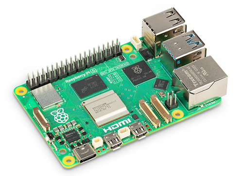
SC1112

Raspberry Pi

$79.61 - $80.00

IN STOCK 10549
Buy

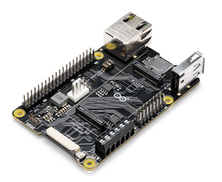
ASX00049

Arduino

* $39.42 - * $44.37

IN STOCK 3123
Buy

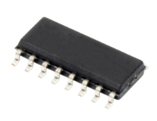
AD96685BRZ

Analog Devices Inc.

$1.72 - * $11.78

IN STOCK 4921
Buy

Reference Designs

RD006

Wurth Elektronik

RD006 - 3 W Dual-output isolated auxiliary supply for communication interfaces and measurement systems

CN0583

Analog Devices Inc.

Multistandard Micropower Verified Smoke Detection System-on-Module

Technical Resources

EVALUATION KITS

EVAL-AD7124-8SDZ

Analog Devices Inc.

$73.86 - * $75.92

IN STOCK 808
Buy
View All