Top Manufacturers
Stock

Displaying 1621 - 1640 of 5440

Evaluation Kits from Analog Devices Inc.

EVAL-AD5932EBZ

Analog Devices Inc.
The AD5932 is a waveform generator offering a programmable frequency scan. Utilizing embedded digital processing that allows enhanced frequency control, the device generates synthesized analog or digital frequency-stepped waveforms. Because frequency profiles are preprogrammed, continuous write cycles are eliminated, thereby freeing up valuable DSP/microcontroller resources. Waveforms start from a known phase and are incremented phase-continuously, which allows phase shifts to be easily determined. Consuming only 6.7 mA, the AD5932 provides a convenient low power solution to waveform generation.The AD5932 outputs each frequency in the range of interest for a defined length of time and then steps to the next frequency in the scan range. The length of time the device outputs a particular frequency is preprogrammed, and the device increments the frequency automatically; or, alternatively, the frequency is incremented externally via the CTRL pin. At the end of the range, the AD5932 continues to output the last frequency until the device is reset. The AD5932 also offers a digital output via the MSBOUT pin.To program the AD5932, the user enters the start frequency, the increment step size, the number of increments to be made, and the time interval that the part outputs each frequency. The frequency scan profile is initiated, started, and executed by toggling the CTRL pin.The AD5932 is written to via a 3-wire serial interface that operates at clock rates up to 40 MHz. The device operates with a power supply from 2.3 V to 5.5 V.Note that the AVDD and DVDD are independent of each other and can be operated from different voltages. The AD5932 also has a standby function that allows sections of the device that are not in use to be powered down.The AD5932 is available in a 16-lead, Pb-free TSSOP.Applications Frequency scanning/radar Network/impedance measurements Incremental frequency stimulus Sensory applications Proximity and motion

EVAL-AD5940ELCZ

Analog Devices Inc.
The AD5940 and AD5941 are high precision, low power analog front ends (AFEs) designed for portable applications that require high precision, electrochemical-based measurement techniques, such as amperometric, voltammetric, or impedance measurements. The AD5940/AD5941 is designed for skin impedance and body impedance measurements, and works with the AD8233 AFE in a complete bioelectric or biopotential measurement system. The AD5940/AD5941 is designed for electrochemical toxic gas sensing.The AD5940/AD5941 consist of two high precision excitation loops and one common measurement channel, which enables a wide capability of measurements of the sensor under test. The first excitation loop consists of an ultra low power, dual-output string, digital-to-analog converter (DAC), and a low power, low noise potentiostat. One output of the DAC controls the noninverting input of the potentiostat, and the other output controls the noninverting input of the transimpedance amplifier (TIA). This low power excitation loop is capable of generating signals from dc to 200 Hz.The second excitation loop consists of a 12-bit DAC, referred to as the high speed DAC. This DAC is capable of generating high frequency excitation signals up to 200 kHz.The AD5940/AD5941 measurement channel features a 16-bit, 800 kSPS, multichannel successive approximation register (SAR) analog-to-digital converter (ADC) with input buffers, a built in antialias filter, and a programmable gain amplifier (PGA). An input multiplexer (mux) in front of the ADC allows the user to select an input channel for measurement. These input channels include multiple external current inputs, external voltage inputs, and internal channels. The internal channels allow diagnostic measurements of the internal supply voltages, die temperature, and reference voltages.The current inputs include two TIAs with programmable gain and load resistors for measuring different sensor types. The first TIA, referred to as the low power TIA, measures low bandwidth signals. The second TIA, referred to as the high speed TIA, measures high bandwidth signals up to 200 kHz.An ultra low leakage, programmable switch matrix connects the sensor to the internal analog excitation and measurement blocks. This matrix provides an interface for connecting external transimpedance amplifier resistors (RTIAs) and calibration resistors. The matrix can also be used to multiplex multiple electronic measurement devices to the same wearable electrodes.A precision 1.82 V and 2.5 V on-chip reference source is available. The internal ADC and DAC circuits use this on-chip reference source to ensure low drift performance for the 1.82 V and 2.5 V peripherals.The AD5940/AD5941 measurement blocks can be controlled via direct register writes through the serial peripheral interface (SPI) interface, or, alternatively, by using a preprogrammable sequencer, which provides autonomous control of the AFE chip. 6 kB of static random access memory (SRAM) is partitioned for a deep data first in, first out (FIFO) and command FIFO. Measurement commands are stored in the command FIFO and measurement results are stored in the data FIFO. A number of FIFO related interrupts are available to indicate when the FIFO is full.A number of general-purpose inputs/outputs (GPIOs) are available and controlled using the AFE sequencer. The AFE sequencer allows cycle accurate control of multiple external sensor devices.The AD5940/AD5941 operate from a 2.8 V to 3.6 V supply and are specified over a temperature range of ?40?C to +85?C. The AD5940 is packaged in a 56-lead, 3.6 mm ? 4.2 mm WLCSP. The AD5941 is packaged in a 48-lead LFCSP.APPLICATIONS Electrochemical measurements Electrochemical gas sensors Potentiostat/amperometric/voltammetry/cyclic voltammetry Bioimpedance applications Skin impedance Body impedance Continuous glucose monitoring Battery impedance

EVAL-AD7091R-4SDZ

Analog Devices Inc.
The AD7091R-2/AD7091R-4/AD7091R-8 family is a multichannel12-bit, ultralow power, successive approximation analog-to-digitalconverter (ADC) that is available in two, four, or eightanalog input channel options. The AD7091R-2/AD7091R-4/AD7091R-8 operate from a single 2.7 V to 5.25 V power supplyand are capable of achieving a sampling rate of 1 MSPS.The AD7091R-2/AD7091R-4/AD7091R-8 family offers up to eightsingle-ended analog input channels with a channel sequencerthat allows a preprogrammed selection of channels to be convertedsequentially. The AD7091R-2/AD7091R-4/ AD7091R-8 alsofeature an on-chip conversion clock, an on-chip accurate 2.5 Vreference, and a high speed serial interface.The AD7091R-2/AD7091R-4/AD7091R-8 have a serial portinterface (SPI) that allows data to be read after the conversionwhile achieving a 1 MSPS throughput rate. The conversion processand data acquisition are controlled using the CONVST pin.The AD7091R-2/AD7091R-4/AD7091R-8 use advanced designtechniques to achieve ultralow power dissipation at highthroughput rates. They also feature flexible power managementoptions. An on-chip configuration register allows the user to set updifferent operating conditions. These include power management,alert functionality, busy indication, channel sequencing, andgeneral-purpose output pins. The MUXOUT and ADCIN pinsallow signal conditioning of the multiplexer output prior toacquisition by the ADC.APPLICATIONS Battery powered systems Personal digital assistants Medical instruments Mobile communications Instrumentation and control systems Data acquisition systems Optical sensors Diagnostic/monitoring functions

EVAL-AD7091R-5SDZ

Analog Devices Inc.
The AD7091R-5 is a 12-bit, multichannel, ultralow power, successive approximation analog-to-digital converter (ADC). The AD7091R-5 operates from a single 2.7 V to 5.25 V power supply and typically consumes only 24 ?A at a 3 V supply in fast mode.?The AD7091R-5 provides a 2-wire serial interface compatible with I2C interfaces. The conversion process can be controlled by a sample mode via the CONVST pin, an autocycle mode selected through software control, or a command mode in which conversions occur across I2C write operations.The device contains a wide bandwidth track-and-hold amplifier that can handle input frequencies up to 1.5 MHz. The AD7091R-5 also features an on-chip conversion clock, an on-chip accurate 2.5 V reference, and a programmable out-of-bounds user alert function.The AD7091R-5 offers four single-ended analog input channels with a channel sequencer that allows a preprogrammed selection of channels to be converted sequentially.The AD7091R-5 uses advanced design techniques to achieve ultralow power dissipation without compromising performance. It also features flexible power management options. An on-chip configuration register allows the user to set up different operating conditions. These include power management, alert functionality, busy indication, channel sequencing, and general-purpose output pins. The MUXOUT and ADCIN pins allow signal conditioning of the multiplexer output before acquisition by the ADC.Applications Battery powered systems Personal digital assistants Medical instruments Mobile communications Instrumentation and control systems Data acquisition systems Optical sensors Diagnostic/monitoring functions

EVAL-AD7091RSDZ

Analog Devices Inc.
The AD7091R is a 12-bit successive approximation analog-to-digitalconverter (ADC) that offers ultralow power consumption(typically 349 ?A at 3 V and 1 MSPS) while achieving fastthroughput rates (1 MSPS with a 50 MHz SCLK). Operatingfrom a single 2.7 V to 5.25 V power supply, the part contains awide bandwidth track-and-hold amplifier that can handle inputfrequencies in excess of 7 MHz. The AD7091R also features anon-chip conversion clock, accurate reference, and high speedserial interface.The conversion process and data acquisition are controlled usinga CONVST signal and an internal oscillator. The AD7091R hasa serial interface that allows data to be read after the conversionwhile achieving a 1 MSPS throughput rate.The AD7091R uses advanced design and process techniques toachieve very low power dissipation at high throughput rates. Anon-chip, accurate 2.5 V reference is availableProduct Highlights Lowest Power 12-Bit SAR ADC Available. On-Chip, Accurate 2.5 V Reference. High Throughput Rate with Ultralow Power Consumption. Flexible Power/Throughput Rate Management. Average power scales with the throughput rate. Power-down mode allows the average power consumption to be reduced when the device is not performing a conversion. Single Supply Operation with VDRIVE Function. The AD7091R operates from a single 2.7 V to 5.25 V supply. The VDRIVE function allows the serial interface to connect directly to 1.8 V to 3.3 V processors.Applications Battery-powered systems ??Handheld meters ??Medical instruments ??Mobile communications Instrumentation and control systems Data acquisition systems Optical sensors Diagnostic/monitoring functions Energy harvesting

EVAL-AD7124-4ASDZ

Analog Devices Inc.
The AD7124-4 is a low power, low noise, completely integrated analog front end for high precision measurement applications. The device contains a low noise, 24-bit ?-? analog-to-digital converter (ADC), and can be configured to have 4 differential inputs or 7 single-ended or pseudo differential inputs. The onchip low gain stage ensures that signals of small amplitude can be interfaced directly to the ADC.One of the major advantages of the AD7124-4 is that it gives the user the flexibility to employ one of three integrated power modes. The current consumption, range of output data rates, and rms noise can be tailored with the power mode selected. The device also offers a multitude of filter options, ensuring that the user has the highest degree of flexibility.The AD7124-4 can achieve simultaneous 50 Hz and 60 Hz rejection when operating at an output data rate of 25 SPS (single cycle settling), with rejection in excess of 80 dB achieved at lower output data rates.The AD7124-4 establishes the highest degree of signal chain integration. The device contains a precision, low noise, low drift internal band gap reference, and also accepts an external differential reference, which can be internally buffered. Other key integrated features include programmable low drift excitation current sources, burnout currents, and a bias voltage generator, which sets the common-mode voltage of a channel to AVDD/2. The low-side power switch enables the user to power down bridge sensors between conversions, ensuring the absolute minimal power consumption of the system. The device also allows the user the option of operating with either an internal clock or an external clock.The integrated channel sequencer allows several channels to be enabled simultaneously, and the AD7124-4 sequentially converts on each enabled channel, simplifying communication with the device. As many as 16 channels can be enabled at any time; a channel being defined as an analog input or a diagnostic such as a power supply check or a reference check. This unique feature allows diagnostics to be interleaved with conversions.The AD7124-4 also supports per channel configuration. The device allows eight configurations or setups. Each configuration consists of gain, filter type, output data rate, buffering, and reference source. The user can assign any of these setups on a channel by channel basis.The AD7124-4 also has extensive diagnostic functionality integrated as part of its comprehensive feature set. These diagnostics include a cyclic redundancy check (CRC), signal chain checks, and serial interface checks, which lead to a morerobust solution. These diagnostics reduce the need for external components to implement diagnostics, resulting in reduced board space needs, reduced design cycle times, and cost savings. The failure modes effects and diagnostic analysis (FMEDA) of a typical application has shown a safe failure fraction (SFF) greater than 90% according to IEC 61508.The device operates with a single analog power supply from 2.7 V to 3.6 V or a dual 1.8 V power supply. The digital supply has a range of 1.65 V to 3.6 V. It is specified for a temperature range of ?40?C to +105?C. The AD7124-4 is housed in a 32-lead LFCSP package or a 24-lead TSSOP package.Applications Temperature measurement? Pressure measurement? Industrial process control? Instrumentation Smart transmitters Smart transmitters

EVAL-AD7170EBZ

Analog Devices Inc.
The AD7170 is a very low power 12-bit analog-to-digital converter (ADC). It contains a precision 12-bit sigma-delta (?-?) ADC and an on-chip oscillator. Consuming only 135 ?A, the AD7170 is particularly suitable for portable or battery operated products where very low power is a requirement. The AD7170 also has a power-down mode in which the device consumes 5 ?A, thus increasing the battery life of the product.For ease-of-use, all the features of the AD7170 are controlled by dedicated pins. Each time a data read occurs, eight status bits are appended to the 12-bit conversion. These status bits contain a pattern sequence that can be used to confirm the validity of the serial transfer.The output data rate of the AD7170 is 125 Hz, whereas the settling time is 24 ms. The AD7170 has one differential input and a gain of 1. This is useful in applications where the user needs to use an external amplifier to implement system-specific filtering or gain requirements.The AD7170 operates with a power supply from 2.7 V to 5.25 V. It is available in a 10-lead LFCSP package.The AD7171 is a 16-bit version of the AD7170. It has the same feature set as the AD7170 and is pin-for-pin compatible.INTERFACE 2-wire serial (read-only device) SPI compatible Schmitt trigger on SCLKAPPLICATIONS Pressure measurement Industrial process control Portable instrumentation

EVAL-AD7298SDZ

Analog Devices Inc.
The AD7298 is a 12-bit, high speed, low power, 8-channel, successive approximation ADC with an internal temperature sensor. The part operates from a single 3.3 V power supply and features throughput rates up to 1 MSPS. The device contains a low noise, wide bandwidth track-and-hold amplifier that can handle input frequencies in excess of 30 MHz.The AD7298 offers a programmable sequencer, which enables the selection of a pre-programmable sequence of channels for conversion. The device has an on-chip 2.5 V reference that can be disabled to allow the use of an external reference.The AD7298 includes a high accuracy band gap temperature sensor, which is monitored and digitized by the 12-bit ADC to give a resolution of 0.25?C. The device offers a 4-wire serial interface compatible with SPI and DSP interface standards.The AD7298 uses advanced design techniques to achieve very low power dissipation at high throughput rates. The part also offers flexible power/throughput rate management options. The part is offered in a 20-lead LFCSP package.PRODUCT HIGHLIGHTS Ideally suited to monitoring system variables in a variety of systems including telecommunications, process and industrial control. High Throughput rate of 1Msps per channel with Low Power Consumption. Eight Single-Ended Inputs with a Channel Sequencer. A consecutive sequence of channels can be selected on which the ADC cycles and converts. Integrated temperature sensor with 0.25?C resolution.

EVAL-AD7328SDZ

Analog Devices Inc.
The AD7328 is an 8-channel, 12-bit plus sign, successive approximation ADC designed on the?iCMOS? (industrial CMOS) process.?iCMOS is a process combining high voltage silicon with submicron CMOS and complementary bipolar technologies. It enables the development of a wide range of high performance analog ICs capable of 33 V operation in a footprint that no previous generation of high voltage parts could achieve. Unlike analog ICs using conventional CMOS processes, iCMOS components can accept bipolar input signals while providing increased performance, dramatically reduced power consumption, and reduced package size.The AD7328 can accept true bipolar analog input signals. The AD7328 has four software-selectable input ranges, ?10 V, ?5 V, ?2.5 V, and 0 V to +10 V. Each analog input channel can be independently programmed to one of the four input ranges. The analog input channels on the AD7328 can be programmed to be single-ended, true differential, or pseudo differential.The ADC contains a 2.5 V internal reference. The AD7328 also allows for external reference operation. If a 3 V reference is applied to the REFIN/OUT pin, the AD7328 can accept a true bipolar ?12 V analog input. Minimum ?12 V VDD and VSS supplies are required for the ?12 V input range. The ADC has a high speed serial interface that can operate at throughput rates up to 1 MSPS.PRODUCT HIGHLIGHTS The AD7328 can accept true bipolar analog input signals, ?10 V, ?5 V, ?2.5 V, and 0 V to +10 V unipolar signals The eight analog inputs can be configured as eight single-ended inputs, four true differential input pairs, four pseudo differential inputs, or seven pseudo differential inputs 1 MSPS serial interface. SPI?-/QSPI?-/DSP-/MICROWIRE?-compatible interface Low power, 30 mW, at a maximum throughput rate of 1 MSPS Channel sequencer

EVAL-AD7356EDZ

Analog Devices Inc.
The AD7356 is a dual, 12-bit, high speed, low power, successive approximation ADC that operates from a single 2.5 V power supply and features throughput rates up to 5 MSPS. The part contains two ADCs, each preceded by a low noise, wide bandwidth track-and-hold circuit that can handle input frequenciesin excess of 110 MHz.The conversion process and data acquisition use standard control inputs allowing for easy interfacing to microprocessors or DSPs. The input signal is sampled on the falling edge of CS; a conversion is also initiated at this point. The conversion time is determined by the SCLK frequency.The AD7356 uses advanced design techniques to achieve very low power dissipation at high throughput rates. With a 2.5 Vsupply and a 5 MSPS throughput rate, the part consumes typically 14 mA. The part also offers a flexible power/throughput rate management option.The analog input range for the part is the differential commonmode ?VREF/2. The AD7356 has an on-chip 2.048 V referencethat can be overdriven when an external reference is preferred.The AD7356 is available in a 16-lead thin shrink small outlinepackage (TSSOP).PRODUCT HIGHLIGHTS Two Complete ADC Functions. These functions allow simultaneous sampling and conversion of two channels. The conversion result of both channels is simultaneously available on separate data lines or in succession on one data line if only one serial port is available. High Throughput with Low Power Consumption. The AD7356 offers a 5 MSPS throughput rate with 36 mW power consumption. No Conversion Latency. The AD7356 features two standard successive approximation ADCs with accurate control of the sampling instant via a CS input and, once off, conversion control.APPLICATIONS Data acquisition systems Motion control I and Q demodulation

EVAL-AD7376EBZ

Analog Devices Inc.
The AD7376 is one of the few high voltage, high performance digital potentiometers on the market. This device can be used as a programmable resistor or resistor divider. The AD7376 performs the same electronic adjustment function as mechanical potentiometers, variable resistors, and trimmers with enhanced resolution, solid-state reliability, and programmability. With digital rather than manual control, the AD7376 provides layout flexibility and allows closed-loop dynamic controllability.The AD7376 features sleep-mode programmability in shutdown that can be used to program the preset before device activation, thus providing an alternative to costly EEPROM solutions.The AD7376 is available in 14-lead TSSOP and 16-lead wide body SOIC packages in 10 k?, 50 k?, and 100 k? options. All parts are guaranteed to operate over the ?40?C to +85?C extended industrial temperature range.APPLICATIONS High voltage DAC Programmable power supply Programmable gain and offset adjustment Programmable filters, delays Actuator control Audio volume control Mechanical potentiometer replacement

EVAL-AD7401AEDZ

Analog Devices Inc.
The AD7401A is a second-order, sigma-delta (?-?) modulatorthat converts an analog input signal into a high speed, 1-bit datastream with on-chip digital isolation based on the AnalogDevices, Inc., iCoupler? technology. The AD7401A operatesfrom a 5 V power supply and accepts a pseudo-differential inputsignal of ?250 mV (?320 mV full scale). The analog input iscontinuously sampled by the analog modulator, eliminating theneed for external sample-and-hold circuitry. The inputinformation is contained in the output stream as a density ofones with a data rate of up to 20 MHz. The original informationcan be reconstructed with an appropriate digital filter. Theserial I/O can use a 5 V or a 3.3 V supply (VDD2).The serial interface is digitally isolated. High speed CMOS,combined with Analog Devices, Inc., iCoupler? technology,means the on-chip isolation provides outstanding performancecharacteristics, superior to alternatives such as optocouplerdevices. The device contains an on-chip reference. TheAD7401A is offered in a 16-lead SOIC and has an operatingtemperature range of ?40?C to +125?C.Applications AC motor controls Shunt current monitoring Data acquisition systems Analog-to-digital and opto-isolator replacements

EVAL-AD7401EDZ

Analog Devices Inc.
The AD7401?is a second-order, sigma-delta (?-?) modulator that converts an analog input signal into a high speed, 1-bit data stream with on-chip digital isolation based on Analog Devices, Inc.,?iCoupler? technology. The AD7401 operates from a 5 V power supply and accepts a differential input signal of ?200 mV (?320 mV full scale). The analog input is continuously sampled by the analog modulator, eliminating the need for external sample-and-hold circuitry. The input information is contained in the output stream as a density of ones with a data rate up to 20 MHz. The original information can be reconstructed with an appropriate digital filter. The serial input/output can use a 5 V or a 3 V supply (VDD2).The serial interface is digitally isolated. High speed CMOS, combined with monolithic air core transformer technology, means the on-chip isolation provides outstanding performance characteristics, superior to alternatives such as optocoupler devices. The device contains an on-chip reference. The AD7401 is offered in a 16-lead SOIC and has an operating temperature range of ?40?C to +105?C.An internal clock version, AD7400, is also available.APPLICATIONS AC motor controls Data acquisition systems A/D + opto-isolator replacements

EVAL-AD7414/15EBZ

Analog Devices Inc.
The AD7414/AD7415 are complete temperature monitoring systems in 6-lead and 5-lead SOT-23 packages. They contain a band gap temperature sensor and a 10-bit ADC to monitor and digitize the temperature reading to a resolution of 0.25?C.The AD7414/AD7415 provide a 2-wire serial interface that is compatible with SMBus and I2C interfaces. The parts come in four versions: the AD7414/AD7415-0, AD7414/AD7415-1, AD7414-2, and AD7414-3. The AD7414/AD7415-0 and AD7414/AD7415-1 versions provide a choice of three different SMBus addresses for each version. All four AD7414 versions give the possibility of eight different I2C addresses while the two AD7415 versions allow up to six I2C addresses to be used.The AD7414/AD7415?s 2.7 V supply voltage, low supply current, serial interface, and small package size make them ideal for a variety of applications, including personal computers, office equipment, cellular phones, and domestic appliances.In the AD7414, on-chip registers can be programmed with high and low temperature limits, and an open-drain overtemperature indicator output (ALERT) becomes active when a programmed?limit is exceeded. A configuration register allows programming of the state of the ALERT output (active high or active low). This output can be used as an interrupt or as an SMBus alert.Applications Hard disk drives Personal computers Electronic test equipment Office equipment Domestic appliances Process control Cellular phones

EVAL-AD7416/7/8EBZ

Analog Devices Inc.
The AD7417 and AD7418 are 10-bit, 4-channel and single-channelADCs with an on-chip temperature sensor that can operate from asingle 2.7 V to 5.5 V power supply. The devices contain a 15 ?ssuccessive approximation converter, a 5-channel multiplexer, atemperature sensor, a clock oscillator, a track-and-hold, and areference (2.5 V). The AD7416 is a temperature-monitoring onlydevice in an 8-lead package.The temperature sensor on the parts can be accessed via multiplexerChannel 0. When Channel 0 is selected and a conversionis initiated, the resulting ADC code at the end of the conversiongives a measurement of the ambient temperature (?1?C @ 25?C).On-chip registers can be programmed with high and low temperaturelimits, and an open-drain overtemperature indicator (OTI)output is provided, which becomes active when a programmedlimit is exceeded.A configuration register allows programming of the sense of theOTI output (active high or active low) and its operating mode(comparator or interrupt). A programmable fault queue counterallows the number of out-of-limit measurements that mustoccur before triggering the OTI output to be set to preventspurious triggering of the OTI output in noisy environments.An I2C? compatible serial interface allows the AD7416/AD7417/AD7418 registers to be written to and read back. The threeLSBs of the AD7416/AD7417 serial bus address can be selected,which allows up to eight AD7416/AD7417 devices to be connectedto a single bus.The AD7417 is available in a narrow body, 0.15 inch, 16-lead,small outline package (SOIC) and in a 16-lead, thin shrink,small outline package (TSSOP). The AD7416 and AD7418 areavailable in 8-lead SOIC and MSOP packages. Product Highlights The AD7416/AD7417/AD7418 have an on-chip temperature sensor that allows an accurate measurement of the ambient temperature (?1?C @ 25?C, ?2?C overtemperature) to be made. The measurable temperature range is ?40?C to +125?C. An overtemperature indicator is implemented by carrying out a digital comparison of the ADC code for Channel 0 (temperature sensor) with the contents of the on-chip TOTI setpoint register. The AD7417 offers a space-saving, 10-bit analog-to-digital solution with four external voltage input channels, an onchip temperature sensor, an on-chip reference, and a clock oscillator. The automatic power-down feature enables the AD7416/ AD7417/AD7418 to achieve superior power performance. At slower throughput rates, the part can be programmed to operate in a low power shutdown mode, allowing further savings in power consumption.Applications Data acquisition with ambient temperature monitoring Industrial process control Automotive Battery-charging applications Personal computers

EVAL-AD7492SDZ

Analog Devices Inc.
The AD7492, AD7492-4, and AD7492-5 are 12-bit high speed, low power, successive approximation ADCs. The parts operate from a single 2.7 V to 5.25 V power supply and feature throughput rates up to 1.25 MSPS. They contain a low noise, wide bandwidth track/hold amplifier that can handle bandwidths up to 10 MHz.The conversion process and data acquisition are controlled using standard control inputs allowing for easy interface to microprocessors or DSPs. The input signal is sampled on the falling edge of CONVST and conversion is also initiated at this point. The BUSY pin goes high at the start of conversion and goes low 880 ns (AD7492/AD7492-4) or 680 ns (AD7492-5) later to indicate that the conversion is complete. There are no pipeline delays associated with the part. The conversion result is accessed via standard CS and RD signals over a high speed parallel interface.The AD7492 uses advanced design techniques to achieve very low power dissipation at high throughput rates. With 5 V supplies and 1.25 MSPS, the average current consumption AD7492-5 is typically 2.75 mA. The part also offers flexible power/throughput rate management.It is also possible to operate the part in a full sleep mode and a partial sleep mode, where the part wakes up to do a conversion and automatically enters a sleep mode at the end of conversion. The type of sleep mode is hardware selected by the PS/FS pin.Using these sleep modes allows very low power dissipation numbers at lower throughput rates.The analog input range for the part is 0 V to REFIN. The 2.5 V reference is supplied internally and is available for external referencing. The conversion rate is determined by the internal clock.PRODUCT HGHLIGHTS High Throughput with Low Power Consumption. The AD7492-5 offers 1.25 MSPS throughput with 16 mW power consumption. Flexible Power/Throughput Rate Management. The conversion time is determined by an internal clock. The part also features two sleep modes, partial and full, to maximize power efficiency at lower throughput rates. No Pipeline Delay. The part features a standard successive approximation ADC with accurate control of the sampling instant via a CONVST input and once-off conversion control. Flexible Digital Interface. The VDRIVE feature controls the voltage levels on the I/O digital pins. Fewer Peripheral Components. The AD7492 optimizes PCB space by using an internal reference and internal CLK. ol { margin-top:0px; margin-right:0px; margin-bottom:0px; margin-left:25px; padding-top:0px; padding-right:0px; padding-bottom:10px; padding-left:0px;} li { padding-top:0px; padding-right:0px; padding-bottom:5px; padding-left:0px; margin-top:0px; margin-right:0px; margin-bottom:0px; margin-left:0px;}

EVAL-AD7605-4SDZ

Analog Devices Inc.
The AD7605-4 is a 4-channel, 16-bit, simultaneous sampling, analog-to-digital data acquisition system (DAS). The device contains analog input clamp protection, a second-order antialias-ing filter, a track-and-hold amplifier, a 16-bit charge redistribution successive approximation analog-to-digital converter (ADC), a 2.5 V reference and reference buffer, and high speed serial and parallel interfaces.The AD7605-4 operates from a single 5 V supply and can accommodate ?10 V and ?5 V true bipolar input signals while sampling at throughput rates of up to 300 kSPS for all channels. The input clamp protection circuitry can tolerate voltages up to ?16.5 V. The AD7605-4 has 1 M? analog input impedance, regardless of sampling frequency. The single-supply operation, on-chip filtering, and high input impedance eliminate the need for driver op amps and external bipolar supplies.The AD7605-4 is SPI, QSPI?, MICROWIRE?, and digital signal processor (DSP) compatible.Applications Power-line monitoring and protection systems Multiphase motor control Instrumentation and control systems Multiaxis positioning systems Data acquisition systems (DAS)

EVAL-AD7606BFMCZ

Analog Devices Inc.
The AD7606B is a 16-bit, simultaneous sampling, analog-to-digital data acquisition system (DAS) with eight channels, each channel containing analog input clamp protection, a programable gain amplifier (PGA), a low-pass filter, and a 16-bit successive approximation register (SAR), analog-to-digital converter (ADC). The AD7606B also contains a flexible digital filter, low drift, 2.5 V precision reference and reference buffer to drive the ADC and flexible parallel and serial interfaces.The AD7606B operates from a single 5 V supply and accommodates ?10 V, ?5 V, and ?2.5 V true bipolar input ranges when sampling at throughput rates of 800 kSPS for all channels. The input clamp protection tolerates voltages up to ?21 V. The AD7606B has a 5 M? analog input impedance, resulting in less than 20 LSB bipolar zero code when the input signal is disconnected and pulled to ground through a 10 k? external resistor. The single supply operation, on-chip filtering, and high input impedance eliminates the need for external driver op amps, which require bipolar supplies. For applications with lower throughput rates, the AD7606B flexible digital filter can be used to improve noise performance.In hardware mode, the AD7606B is fully compatible with the AD7606. In software mode, the following advanced features are available: Additional ?2.5 V analog input range. Analog input range (?10 V, ?5 V, and ?2.5 V), selectable per channel. Additional oversampling (OS) options, up to OS ? 256. System gain, system offset, and system phase calibration per channel. Analog input open circuit detector. Diagnostic multiplexer. Monitoring functions (serial peripheral interface (SPI) invalid read/write, cyclic redundancy check (CRC), overvoltage and undervoltage events, busy stuck monitor, and reset detection).Note that throughout this data sheet, multifunction pins, such as the RD/SCLK pin, are referred to either by the entire pin name or by a single function of the pin, for example, the SCLK pin, when only that function is relevant.Applications Power line monitoring Protective relays Multiphase motor control Instrumentation and control systems Data acquisition systems

EVAL-AD7626FMCZ

Analog Devices Inc.
The AD7626 is a 16-bit, 10 MSPS, charge redistributionsuccessive approximation register (SAR) based architectureanalog-to-digital converter (ADC). SAR architecture allowsunmatched performance both in noise (91.5 dB SNR) and inlinearity (?0.45 LSB INL). The AD7626 contains a high speed,16-bit sampling ADC, an internal conversion clock, and aninternal buffered reference. On the CNV edge, it samples thevoltage difference between the IN+ and IN? pins. The voltageson these pins swing in opposite phase between 0 V and REF.The 4.096 V reference voltage, REF, can be generated internallyor applied externally.All converted results are available on a single low voltagedifferential signaling (LVDS) self clocked or echoed clock serialinterface, reducing external hardware connections.The AD7626 is housed in a 32-lead, 5 mm ? 5 mm LFCSP withoperation specified from ?40?C to +85?C.Applications Digital imaging systems ??Digital X-ray ??Digital MRI ? CCD and IR cameras High speed data acquisition High dynamic range telecommunications receivers Spectrum analysis Test equipment

EVAL-AD7655EDZ

Analog Devices Inc.
The AD7655 is a low cost, simultaneous sampling, dual-channel,16-bit, charge redistribution SAR, analog-to-digital converterthat operates from a single 5 V power supply. It contains twolow noise, wide bandwidth, track-and-hold amplifiers that allowsimultaneous sampling, a high speed 16-bit sampling ADC, aninternal conversion clock, error correction circuits, and bothserial and parallel system interface ports. Each track-and-holdhas a multiplexer in front to provide a 4-channel input ADC.The A0 multiplexer control input allows the choice ofsimultaneously sampling input pairs INA1/INB1 (A0 = low) orINA2/INB2 (A0 = high). The part features a very high samplingrate mode (normal) and, for low power applications, a reducedpower mode (impulse) where the power is scaled with thethroughput. Operation is specified from ?40?C to +85?C.Product Highlights Multichannel ADC. The AD7655 features 4-channel inputs with two sample-and-hold circuits that allow simultaneous sampling. Fast Throughput. The AD7655 is a 500 kSPS, charge redistribution, 16-bit SAR ADC with internal error correction circuitry. Single-Supply Operation. The AD7655 operates from a single 5 V supply. In impulse mode, its power dissipation decreases with throughput. Serial or Parallel Interface. Versatile parallel or 2-wire serial interface arrangements are compatible with both 3 V and 5 V logic.Applications AC motor control 3-phase power control 4-channel data acquisition Uninterrupted power supplies Communications

Displaying 1621 - 1640 of 5440

Latest Parts

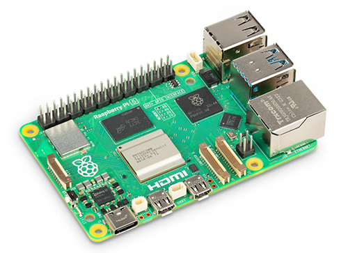
SC1112

Raspberry Pi

$80.00 - $80.01

IN STOCK 4910
Buy

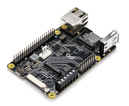
ASX00049

Arduino

* $33.67 - * $42.28

IN STOCK 3002
Buy
IN STOCK 4682
Buy

Reference Designs

RD006

Wurth Elektronik

RD006 - 3 W Dual-output isolated auxiliary supply for communication interfaces and measurement systems

CN0583

Analog Devices Inc.

Multistandard Micropower Verified Smoke Detection System-on-Module

Technical Resources

EVALUATION KITS

EVAL-AD7124-8SDZ

Analog Devices Inc.

$63.71 - * $75.48

IN STOCK 794
Buy
View All