Manufacturer
Stock

Displaying 1641 - 1660 of 5422

Evaluation Kits from Analog Devices Inc.

EVAL-AD5680EBZ

Analog Devices Inc.
Data Conversion IC Development Tools EVAL BRD AD5680

LTC4070EDDB Demo Board | Simple Low-IQ Battery Charger/Protector with NTC Thermistor Input

Analog Devices Inc.
DC1584A: Demo Board for the LTC4070 Li-Ion/Polymer Shunt Battery Charger System.

DC2002A

Analog Devices Inc.
The LTC3774 is a dual PolyPhase? current mode synchronous step-down switching regulator controller that drives power blocks, DRMOS or external gate drivers and power MOSFETs. It offers an LTC-proprietary technique that enhances the signal-to-noise ratio of the current sense signal, allowing the use of inductors with very low DC winding resistances as the current sense element for maximum efficiency and reduced jitter.The maximum current sense voltage is programmable from 10mV to 30mV. High speed, low offset remote sense differential amplifiers and a precise 0.6V reference provide accurate output voltages between 0.6V and 3.5V from a wide 4.5V to 38V input supply range. Soft recovery from output shorts or overcurrent minimizes output overshoot. Burst Mode? operation, continuous and pulse-skipping modes are supported. The constant operating frequency can be synchronized to an external clock or linearly programmed from 200kHz to 1.2MHz. Up to six LTC3774 controllers can be paralleled for 1-, 2-, 3-, 4-, 6-, 8- or 12-phase operation.The LTC3774 is available in a 36-lead (5mm ? 6mm) QFN package.Applications Computer Systems Telecom and Datacom Systems Industrial Equipment DC Power Distribution Systems

DC2815A

Analog Devices Inc.
The LT3120 is a high efficiency 26V monolithic buck-boost converter. Extensive feature integration and very low resistance internal power switches minimize the total solution footprint for even the most demanding applications. A proprietary 4-switch PWM architecture provides seamless low noise operation from input voltages above, equal to, or below the output voltage.External frequency programming as well as synchronization using an internal PLL enable operation over a wide switching frequency range of 400kHz to 2MHz. The wide 2.5V to 26V input range is well suited for operation from unregulated power sources including battery stacks and backup capacitors. After start-up, operation is possible with input voltages as low as 500mV.Other features include, output short-circuit protection, thermal overload protection, less than 3?A shutdown current, power good indicator, Burst Mode operation, and maximum power point control.The LT3120 is offered in thermally enhanced 28-lead 4mm ? 5mm LQFN package.APPLICATIONS RF Power Supply USB Power Delivery System Backup Power Supply 1-Cell to 5-Cell Lithium Battery Powered Products Wide Input Range Power Supply Lead Acid to 12V Regulator

DC2895A

Analog Devices Inc.
The LT7101 is a high efficiency, monolithic synchronous step-down DC/DC converter utilizing a constant frequency, average current mode control architecture. It operates from an input voltage range of 4.4V to 105V and provides an adjustable regulated output voltage from 1V to VIN while delivering up to 1A of output current.?The LT7101 features high frequency operation and a low minimum on-time that reduce inductor size and enable constant-frequency operation even at very high stepdown ratios. In addition, the LT7101 achieves the lowest possible dropout voltage with 100% maximum duty cycle operation. During light load operation, converter efficiency and output ripple can be optimized by selecting Burst Mode, pulse-skipping or forced continuous operation.The LT7101 includes accurate, high speed average current programming and monitoring without the need for an external sense resistor. Additional features include a bypass LDO to maximize efficiency, fixed or adjustable output voltage and loop compensation, and a wide array of protection features to enhance reliability.?Applications Battery Chargers and CC/CV Supplies Automotive and Military Systems Industrial, Avionics and Heavy Equipment Medical Instruments and Telecommunication Systems

DC954B-C

Analog Devices Inc.
The LT6402-20 is a low distortion, low noise differential ampli?er/ADC driver for use in applications from DC to 300MHz. The LT6402-20 has been designed for ease of use, with minimal support circuitry required. Exceptionally low input-referred noise and low distortion (with either single-ended or differential inputs) make the LT6402-20 an excellent solution for driving high speed 12-bit and 14-bit ADCs. In addition to the normal unfiltered outputs (+OUT and ?OUT), the LT6402-20 has a built-in 75MHz differential low pass filter and an additional pair of filtered outputs (+OUTFILTERED, ?OUTFILTERED) to reduce external filtering components when driving high speed ADCs. The output common mode voltage is easily set via the VOCM pin, eliminating an output transformer or AC-coupling capacitors in many applications.The LT6402-20 is designed to meet the demanding requirements of communications transceiver applications. It can be used as a differential ADC driver, a general-purpose differential gain block, or in other applications requiring differential drive. The LT6402-20 can be used in data acquisition systems required to function at frequencies down to DC.The LT6402-20 operates on a 5V supply and consumes 30mA. It comes in a compact 16-lead 3mm ? 3mm QFN package and operates over a ?40?C to 85?C temperature range.Applications Differential ADC Driver for: Imaging Communications Differential Driver/Receiver Single Ended to Differential Conversion Differential to Single Ended Conversion Level Shifting IF Sampling Receivers SAW Filter Interfacing/Buffering

EV1HMC589AST89

Analog Devices Inc.
The HMC589AST89E is an InGaP HBT Gain Block MMIC SMT amplifier covering DC to 4 GHz and packaged in an industry standard SOT89E. The amplifier can be used as a cascadable 50 Ohm RF or IF gain stage as well as a LO or PA driver with up to +19 dBm P1dB output power for cellular/3G, FWA, CATV, microwave radio and test equipment applications. The HMC589AST89E offers 20 dB gain and +33 dBm output IP3 at 1 GHz while requiring only 82 mA from a single positive supply. The HMC589AST89E InGaP HBT gain block offers excellent output power and gain stability over temperature.APPLICATIONSCellular / PCS / 3GFixed Wireless & WLANCATV, Cable Modem & DBSMicrowave Radio & Test EquipmentIF & RF Applications

EV-ADF4372SD2Z

Analog Devices Inc.
The ADF4372 allows implementation of fractional-N or integer-N phase-locked loop (PLL) frequency synthesizers when used with an external loop filter and an external reference frequency. The wideband microwave voltage controlled oscillator (VCO) design allows frequencies from 62.5 MHz to 16 GHz to be generated.The ADF4372 has an integrated VCO with a fundamental output frequency ranging from 4000 MHz to 8000 MHz. In addition, the VCO frequency is connected to a divide by 1, 2, 4, 8, 16, 32, or 64 circuit that allows the user to generate radio frequency (RF) output frequencies as low as 62.5 MHz at RF8x. A frequency multiplier at RF16x generates from 8 GHz to 16 GHz. RFAUX8x duplicates the frequency range of RF8x or permits direct access to the VCO output. To suppress the unwanted products of frequency multiplication, a harmonic filter exists between the multiplier and the output stage of RF16x.Control of all on-chip registers is through a 3-wire interface. The ADF4372 operates with analog and digital power supplies ranging from 3.15 V to 3.45 V, and 5 V for the VCO power supply. The ADF4372 also contains hardware and software power-down modes.APPLICATIONS Wireless infrastructure (multicarrier global system for mobile communication (MC-GSM), 5 G) Test equipment and instrumentation Clock generation Aerospace and defense

EV-ADF5709

Analog Devices Inc.
The ADF5709 wideband, monolithic microwave integrated circuit (MMIC), voltage controlled oscillator (VCO) supports an output frequency (fOUT) range of 9.85 GHz to 20.5 GHz while maintaining ?83 dBc/Hz phase noise at 100 kHz offset without subharmonic tones. The wide frequency tuning range and low phase noise allow phase-locked loop (PLL) solutions for a variety of frequency bands and limit the need for multiple narrow-band VCOs. The broad frequency coverage reduces the board design complexity and simplifies the bill of materials when designing RF and microwave applications.The VCO operates from a single 5 V supply and consumes only 70 mA of supply current that results in minimal power dissipation. The ADF5709 low power consumption is ideal for high performance applications with limited or no airflow. The monolithic construction of the VCO allows optimal output power and noise characteristics over temperature variations.The VCO is fully integrated and incorporates a resonator, a negative resistance device, and a varactor diode that minimize the number of external components and reduces board space.The low input impedance on the VTUNE pin of the ADF5709 enables high tuning speed and modulation bandwidth, which allows faster frequency sweeps and lock times when used as part of a frequency synthesizer, for example, in radar or in test and measurement applications.The ADF5709 is encapsulated into a tiny, 3.90 mm ? 3.90 mm, RoHS compliant, ceramic leadless chip carrier (LCC) package. The package includes through vias to the exposed pad, enhancing thermal characteristics.The small size, optimal noise performance, low power consumption, and wide tuning range of the ADF5709 make the device ideal for many applications requiring flexibility, high performance, a small footprint, and a tight power budget. The ADF5709 is pin to pin compatible with the HMC733 and other Analog Devices, Inc., wideband VCOs.APPLICATIONSIndustrial and medical equipmentTest and measurement equipmentMilitary radars, electronic warfare (EW), and electronic countermeasures (ECMs)Point to point and multipoint radiosVery small aperture terminals (VSATs)Wireless communication infrastructure

EVAL-ADAQ23875FMCZ

Analog Devices Inc.
The ADAQ23875 is a precision, high speed, ?Module? data acquisition solution that reduces the development cycle of a precision measurement systems by transferring the design burden of component selection, optimization, and layout from the designer to the device.Using system-in-package (SIP) technology, the ADAQ23875 reduces end system component count by combining multiple common signal processing and conditioning blocks in a single device, solving many design challenges. These blocks include a low noise, fully differential analog-to-digital converter (ADC) driver (FDA), a stable reference buffer, and a high speed, 16-bit, 15 MSPS successive approximation register (SAR) ADC.Using Analog Devices, Inc., iPassives? technology, the ADAQ23875 also incorporates crucial passive components with superior matching and drift characteristics to minimize temperature dependent error sources and to offer optimized performance (see Figure 1). The fast settling of the ADC driver stage, with fully differential or single-ended to differential input and no latency of the SAR ADC, provides a unique solution for high channel count multiplexed signal chain architectures and control loop applications.The small footprint, 9 mm ? 9 mm CSP_BGA package enables smaller form factor instruments without sacrificing performance. Single, 5 V supply operation is possible while achieving optimum performance from the device. The ADAQ23875 features a serial low voltage differential signaling (LVDS) digital interface with one-lane or two-lane output modes, allowing the user to optimize the interface data rate for each application. The specified operation of the ?Module is from ?40?C to +85?C.APPLICATIONSATEData acquisitionHardware in the Loop (HiL)Power analyzersNondestructive test (acoustic emissions)Mass spectrometryTravelling wave fault locationMedical imaging and instrumentsUltrasonic flow meters

EVAL-ADF4150EB1Z

Analog Devices Inc.
The ADF4150 allows implementation of fractional-N or integer-N phase-locked loop (PLL) frequency synthesizers if used with an external voltage-controlled oscillator (VCO), loop filter, and external reference frequency.The ADF4150 is for use with external VCO parts and is software compatible with the ADF4350. The VCO frequency can be divided by 1/2/4/8/16 to allow the user to generate RF output frequencies as low as 31.25 MHz. For applications that require isolation the RF output stage can be muted. The mute function is both pin and software controllable.Control of all the on-chip registers is through a simple 3-wire interface. The device operates with a power supply ranging from 3.0 V to 3.6 V and can be powered down when not in use.The ADF4150 is available in a 4 mm ? 4 mm package.Applications Wireless infrastructure (W-CDMA, TD-SCDMA, WiMax, GSM, PCS, DCS, DECT) Test equipment Wireless LANs, CATV equipment Clock generation

EVAL-ADN4693E-1EBZ

Analog Devices Inc.
The ADN4693E-1 is a multipoint, low voltage differential signaling (M-LVDS) transceiver (driver and receiver pair) that can operate at up to 200 Mbps (100 MHz) nonreturn to zero (NRZ). The receiver detects the bus state with a differential input of as little as ?50 mV over the common-mode voltage range of the device. Electrostatic discharge (ESD) protection of up to ?15 kV is implemented on the bus pins. The ADN4693E-1 is designed to the TIA/EIA-899 standard for M-LVDS and complement TIA/EIA-644 LVDS devices with additional multipoint capabilities.The ADN4693E-1 features a Type 1 receiver with 25 mV of hysteresis so that slow-changing signals or loss of input does not lead to output oscillations.This full-duplex device is available in a compact 16-lead, 4 mm ? 4 mm lead frame chip scale package (LFCSP). The ADN4693E-1 is specified over the -40?C to +120?C junction temperature range.APPLICATIONS Backplane and cable multipoint data transmission Multipoint clock distribution Low power, high speed alternative to shorter RS-485 links Networking and wireless base station infrastructure Grid infrastructure and relay protection systems

EV-RAPID-ESL2-433Z

Analog Devices Inc.
The ADuCM3027/ADuCM3029 microcontroller units (MCUs) are ultra low power microcontroller systems with integrated power management for processing, control, and connectivity. The MCU system is based on the ARM? Cortex?-M3 processor, a collection of digital peripherals, embedded SRAM and flash memory, and an analog subsystem which provides clocking, reset, and power management capability in addition to an analog-to-digital converter (ADC) subsystem. For a feature comparison across the ADuCM3027/ADuCM3029 product offerings, see Table 1. Table 1. Product Flash Memory Options Device Embedded Flash Memory Size ADuCM3029 256 kB ADuCM3027 128 kB System features that are common across the ADuCM3027/ADuCM3029/ADuCM3029-1/ADuCM3029-2 MCUs include the following: Up to 26 MHz ARM Cortex-M3 processor Up to 256 kB of embedded flash memory with error correction code (ECC) Optional 4 kB cache for lower active power 64 kB system SRAM with parity Power management unit (PMU) Multilayer advanced microcontroller bus architecture (AMBA) bus matrix Central direct memory access (DMA) controller Beeper interface Serial port (SPORT), serial peripheral interface (SPI), inter-integrated circuit (I2C), and universal asynchronous receiver/transmitter (UART) peripheral interfaces Cryptographic hardware support with advanced encryption standard (AES) and secure hash algorithm (SHA)-256 Real-time clock (RTC) General-purpose and watchdog timers Programmable general-purpose input/output (GPIO) pins Hardware cyclic redundancy check (CRC) calculator with programmable generator polynomial Power-on reset (POR) and power supply monitor (PSM) 12-bit successive approximation register (SAR) ADC True random number generator (TRNG)To support low dynamic and hibernate power management, the ADuCM3027/ADuCM3029 MCUs provide a collection of power modes and features, such as dynamic and software controlled clock gating and power gating.The ADuCM3029-1 and ADuCM3029-2 MCU models share the same features and functionality as that of the ADuCM3029 MCU. All specifications pertaining to the ADuCM3027 and ADuCM3029 are also applicable to the ADuCM3029-1 and ADuCM3029-2.For full details on the ADuCM3027/ADuCM3029 MCUs, refer to the ADuCM302x Ultra Low Power ARM Cortex-M3 MCU with Integrated Power Management Hardware Reference Manual.Product Highlights Industry leading ultralow power consumption. Robust operation, including full voltage monitoring in deep sleep modes, ECC support on flash, and parity error detection on SRAM memory. Leading edge security. Fast encryption provides read protection to customer algorithms. Write protection prevents device reprogramming by unauthorized code. Failure detection of 32 kHz LFXTAL via interrupt. SensorStrobe? for precise time synchronized sampling of external sensors. Works in hibernate mode, resulting in drastic current reduction in system solutions. Current consumption reduces by 10 times when using, for example, the ADXL363 accelerometer. Software intervention is not required after setup. No pulse drift due to software execution.Applications Internet of Things (IoT) Electronic shelf label (ESL) and signage Smart infrastructure Smart lock Asset tracking Smart machine, smart metering, smart building, smart city, and smart agriculture Wearables Fitness and clinical Machine learning and neural network?

LT3471 Signal Chain Evaluation Board | Dual Boost/Inverting Converter

Analog Devices Inc.
Demonstration circuit SCP-LT3471-EVALZ is a dual output converter featuring the LT3471EDD in boost and inverter configurations. Both converters are powered from the same 4.5V to 10V input source. The Boost converter puts out 12V at 300mA and the Inverter –12V at 200mA. Like all boards in the Signal Chain Power series, this board is designed to be easily plugged into other SCP boards to form a complete signal chain power system, enabling fast evaluation of low power signal chains. To evaluate this board, some universal SCP hardware is required, namely: SCP-INPUT-EVALZ SCP-OUTPUT-EVALZ SCP-1X5BKOUT-EVALZ SCP-THRUBRD-EVALZ SCP-FILTER-EVALZ SCP-1X2BKOUT-EVALZ SCP-5X1-EVALZ   To properly evaluate SCP series demo boards, you will need the SCP Configurator companion software. SCP Configurator can help you choose the right board and topology for your design. Note that the Demo Manual does not cover details important to the operation and configuration regarding the LT3471. Please refer to the LT3471 data sheet for a complete description of the part.

MAX5391LEVMINIQU+

Analog Devices Inc.
Digital Potentiometer Development Tools Eval Kit/System MAX5386M, MAX5388, MAX5391, and MAX5393 (Dual 256-Tap,Volatile, Low-Voltage Linear Taper Digital Potentiometers)

EV-DNG-RFMOD-9001Z

Analog Devices Inc.
The ADF7023 is a very low power, high performance, highly integrated 2FSK/GFSK/OOK/MSK/GMSK transceiver designed for operation in the 862 MHz to 928 MHz and 431 MHz to 464 MHz frequency bands, which cover the worldwide license-free ISM bands at 433 MHz, 868 MHz, and 915 MHz. It is suitable for circuit applications that operate under the European ETSI EN300-220, the North American FCC (Part 15), the Chinese short-range wireless regulatory standards, or other similar regional standards. Data rates from 1 kbps to 300 kbps are supported.The transmit RF synthesizer contains a VCO and a low noise fractional-N PLL with an output channel frequency resolution of 400 Hz. The VCO operates at 2? or 4?, the fundamental frequency to reduce spurious emissions. The receive and transmit synthesizer bandwidths are automatically, and independently, configured to achieve optimum phase noise, modulation quality, and settling time. The transmitter output power is programmable from ?20 dBm to +13.5 dBm, with automatic PA ramping to meet transient spurious specifications. The part possesses both single-ended and differential PAs, which allows for Tx antenna diversity.The receiver is exceptionally linear, achieving an IP3 specification of ?12.2 dBm and ?11.5 dBm at maximum gain and minimum gain, respectively, and an IP2 specification of 18.5 dBm and 27 dBm at maximum gain and minimum gain, respectively. The receiver achieves an interference blocking specification of 66 dB at ?2 MHz offset and 74 dB at ?10 MHz offset. Thus, the part is extremely resilient to the presence of interferers in spectrally noisy environments. The receiver features a novel, high speed, automatic frequency control (AFC) loop, allowing the PLL to find and correct any RF frequency errors in the recovered packet.A patent pending, image rejection calibration scheme is available through a program download. The algorithm does not require the use of an external RF source nor does it require any user intervention once initiated. The results of the calibration can be stored in nonvolatile memory for use on subsequent power-ups of the transceiver.See data sheet for additional information.Applications Smart metering IEEE 802.15.4g Wireless MBUS Home automation Process and building control Wireless sensor networks (WSNs) Wireless healthcare

EV-COG-LTP5902Z

Analog Devices Inc.
SmartMesh IP wireless sensor networks are self managing, low power internet protocol (IP) networks built from wireless nodes called motes.The LTP5902-IPM is printed circuit board assembly (PCBA) product with on-board chip antenna in the Eterna? family of IEEE 802.15.4e solutions, featuring a highly integrated, low power radio design as well as an ARM Cortex-M3 32-bit microprocessor running SmartMesh IP embedded networking software. The LTP5902-IPM, at 37mm ? 24mm, is built for surface-mount assembly.With SmartMesh IP time-synchronized networks, all motes in the network may route, source or terminate data, while providing many years of battery powered operation. SmartMesh IP is a highly flexible network with proven reliability and low power performance in an easy-to-integrate platform.The LTP5902-IPM?s behavior in a SmartMesh IP network is determined by the choice of SmartMesh IP network software loaded: Wireless Mote, EManager, Access Point Mote in a SmartMesh IP network. The SmartMesh IP software provided with the LTP5902-IPM is fully tested and validated, and is readily configured via a software Application Programming Interface. Once you have purchased SmartMesh IP products, the SmartMesh IP stack binaries may be downloaded via your myAnalog account. The pin signaling behavior of the LTP5902IPC-IPMA hardware is determined by the software loaded and is described in detail in the following product datasheets: LTP5902-IPM = LTP5902IPC-IPMA hardware + SmartMesh IP ?Mote? Software ? LTP5902-IPM Datasheet LTP5902-IPR = LTP5902IPC-IPMA hardware + SmartMesh IP EManager Software ? LTP5902-IPR Datasheet LTP5902-IPA = LTP5902IPC-IPMA hardware + SmartMesh IP Access Point Software ? LTP5902-IPA Datasheet Network Features Feature Benefit >99.999% Network Reliability Avoids communications dropouts common with other wireless networks NIST-certified AES-128 bit Encryption Data protected by end-to-end encryption, message integrity checking and device authentication Scalable Uses time-slotted channel-hopping protocol to avoid in-network collisions to maximize scale while minimizing power and latency-hungry transmission retries due to congestion Bidirectional Communications Ideal for both monitoring and control applications Up to 10 messages/second/node Time-slotted communications avoids contention. This data rate includes built-in margin for packet retries. Device Features Feature Benefit Industry-Leading Low Power Radio Technology ? 4.5mA to Receive a Packet ? 5.4mA to Transmit at 0dBm ? 9.7mA to Transmit at 8dBm Pre-engineered RF RF elements include an on-chip power amplifier and are pre-tuned for optimized performance, including temperature compensation, saving development time. RF Modular Certifications Pre-certified in USA, Canada, EU, Australia/New Zealand, India, Japan, Korea, Taiwan Energy Harvesting Support Very low power design enables motes to be powered by a wide variety of energy harvesters. Click here to see a demonstration circuit of a SmartMesh IP mote powered by indoor light. Integrated Temperature Sensor Precise temperature sensor is integrated directly into the mote. ApplicationsSmartMesh IP is ideally suited for wireless Industrial Internet of Things (IoT) applications. To learn more about SmartMesh applications, click here.

EV-ADF4360-4EB1Z

Analog Devices Inc.
The ADF4360-4 is a fully integrated integer-N synthesizerand voltage-controlled oscillator (VCO). The ADF4360-4 isdesigned for a center frequency of 1600 MHz. In addition, adivide-by-2 option is available, whereby the user gets an RFoutput of between 725 MHz and 875 MHz.Control of all the on-chip registers is through a simple 3-wireinterface. The device operates with a power supply rangingfrom 3.0 V to 3.6 V and can be powered down when not in use.Applications Wireless handsets (DECT, GSM, PCS, DCS, WCDMA) Test equipment Wireless LANs CATV equipment

EVAL-ADUM4177EBZ

Analog Devices Inc.
The ADuM4177 is an advanced isolated gate driver that provides 5 kVrms isolation employing Analog Devices, Inc. iCouper? technology. The ADuM4177 provides 8.3 mm creepage in a 28-pin wide body SOIC package. The devices are suitable for applications that require insulation against working voltages of 1060 V rms and 1500 V dc for the lifetime of the device. Combining high speed CMOS and monolithic transformer technology, these isolated gate drivers provide outstanding performance characteristics suitable for driving the demanding needs of high performance Silicon Carbide (SiC) switches. SPI communication allows for user programmable operating modes and fault read back.The ADuM4177 operates with an input voltage range from 4.4 to 7 V. The output voltages can operate with bipolar gate drive of 12 to 24 V positive and -5.5 to -3.25 V for the negative rail. Multiple programmable undervoltage lockout (UVLO) levels can be obtained through SPI communication with the gate driver. In comparison to gate drivers employing high voltage level translation methodologies, the ADuM4177 offers the benefit of true, galvanic isolation between the input and the output.The ADuM4177 includes many advanced protection features such as the drain monitoring desaturation detection, an active short circuit (ASC) operation, external temperature sensing, and both over voltage protection (OVP) and undervoltage protection (UVP).Adjustable slew rate control is available to allow for faster edge transitions and higher efficiency when the system operating point can accommodate it. An external miller clamp allows for strong pull-down to prevent unintended Miller injection induced turn on. The ADuM4177 can operate in a wide range of junction temperatures, from -40 to 150?C.As a result, the ADuM4177 provides reliable control over the switching characteristics of SiC switch configurations over a wide range of switching voltages.APPLICATIONSSwitching power suppliesSiC gate driversIndustrial invertersPower Factor Correctors

Displaying 1641 - 1660 of 5422

Latest Parts

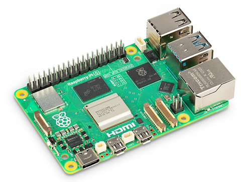
SC1112

Raspberry Pi

$79.61 - $80.00

IN STOCK 10488
Buy

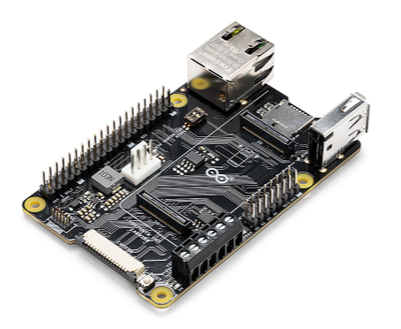
ASX00049

Arduino

* $39.42 - * $44.37

IN STOCK 3123
Buy

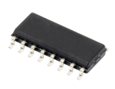
AD96685BRZ

Analog Devices Inc.

$1.72 - * $11.78

IN STOCK 4921
Buy

Reference Designs

RD006

Wurth Elektronik

RD006 - 3 W Dual-output isolated auxiliary supply for communication interfaces and measurement systems

CN0583

Analog Devices Inc.

Multistandard Micropower Verified Smoke Detection System-on-Module

Technical Resources

EVALUATION KITS

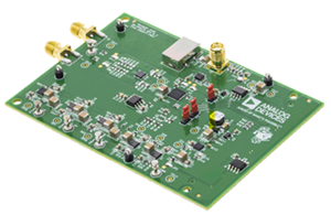
EVAL-AD7124-8SDZ

Analog Devices Inc.

$71.02 - * $75.92

IN STOCK 808
Buy
View All