
LTC1682CMS8 | Doubler Charge Pump with Linear Regulator, Adjustable, 1.8 to 4.4VIN, 2.5 to 5.5VOUT @ 50mA
Analog Devices Inc.DC249A-A: Demo Board for the LTC1682 Doubler Charge Pumps with Low Noise Linear Regulator.
LTC1682CMS8-5 | Doubler Charge Pump with Linear Regulator, Fixed, 2.7 to 4.4VIN, 5.0VOUT @ 50mA
Analog Devices Inc.DC249A-B: Demo Board for the LTC1682 Doubler Charge Pumps with Low Noise Linear Regulator.

LTM8002 40VIN, 2.5A Step-Down µModule Regulator
Analog Devices Inc.Demonstration circuit 2501A features the LTM®8002, a 40V, 2.5A step-down µModule® regulator. This demo circuit is configured to deliver a 5.0V output from an input
voltage between…

DC2504A
Analog Devices Inc.The LT8630 is a current mode PWM step-down DC/DC converter with internal synchronous switches that provide current for output loads up to 0.6A. The wide input range of 3V to 100V…

LTC1503CMS8-2 | High Efficiency Inductorless Step-Down DC/DC Converter, 2.4 to 6VIN, 2VOUT @ 100mA
Analog Devices Inc.DC250A-A: Demo Board for the LTC1503 High Efficiency Inductorless Step-Down DC/DC Converter.

LTC2975 Demo Board: ±12V, ±48V Power Supply Management [requires DC1613]
Analog Devices Inc.The DC2518A is a demonstration system for the LTC2975 Power System Manager that interfaces to various regulators. The board contains all the circuitry needed to use the LTC2975 in…

DC2527A-B
Analog Devices Inc.The LTM4646 is a complete dual 10A output switching mode DC/DC power supply. Included in the package are the switching controller, power FETs, inductors, and all supporting…

LTC7810ELXE High Input Voltage Dual Output Synchronous Buck Converter
Analog Devices Inc.Demonstration circuit 2529A is a dual output synchronous buck converter featuring the LTC7810ELXE in a 48-lead eLQFP package.
Key features of this board include: an optional…
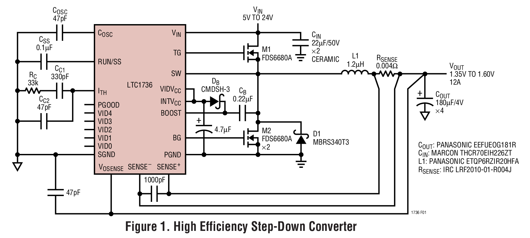
LTC1736CG | 5 Bit, VID CPU Power Converter, VIN = 5V to 24V, VOUT = 0.9V to 2.0V @ 12A
Analog Devices Inc.DC252A: Demo Board for the LTC1736 5-Bit Adjustable High Efficiency Synchronous Step-Down Switching Regulator.

LTC2986 Demo Board | LTC2986 Motherboard (DC2508) + 20-Input Breakout Board (DC2210), Requires DC2026
Analog Devices Inc.The DC2531 is the starter kit for demonstrating the performance and ease of use of the LTC2986, which is a complete temperature measurement system on a chip. This kit includes the…

LTM4678 Demo Board | Dual 25A or Single 50A μModule Regulator with Digital Power System Management
Analog Devices Inc.Demonstration circuit 2552A is a dual-output, high efficiency, high density, µModule regulator with 4.5V to 16V input range. Each output can supply 25A maximum load current. The…

LTM4661EY Demo Board | 1.8V-5.5V Input, Synchronous Step-Up μModule Regulator
Analog Devices Inc.Demonstration circuit 2569A is ultrathin step-up μModule regulator featuring the LTM4661. The DC2569A operates over 1.8V to 5.5V input and it generates 12V, 1A output from 5V…

DC2581A-A
Analog Devices Inc.The LTC2341-18 is an 18-bit, low noise 2-channel simultaneous sampling successive approximation register (SAR) ADC with differential, wide common mode range inputs. Operating from…

LT4295/LT4321 Demo Board | PoE++ (71W/12V/5.5A) PD with Forward DC/DC and Ideal Diode Bridge
Analog Devices Inc.Demonstration circuit 2584A is an IEEE 802.3bt (Draft 2.1) compliant Power over Ethernet (PoE) Powered Device (PD). It features the LT4295 PD interface and switching regulator…

DC2588A-A
Analog Devices Inc.The LTC2387-18 is a low noise, high speed, 18-bit 15Msps successive approximation register (SAR) ADC ideally suited for a wide range of applications. The combination of excellent…

EVAL-AD7767-1EDZ
Analog Devices Inc.The AD7767/AD7767-1/AD7767-2 are high performance, 24-bit, oversampled SAR analog-to-digital converters (ADCs). The AD7767/AD7767-1/AD7767-2 combine the benefits of a large…

EVAL-AD7785EBZ
Analog Devices Inc.The AD7785 is a low power, low noise, complete analog front ends for high precision measurement applications. It contains a low noise 20-bit ?-? ADC with three differential analog…

EVAL-AD7796EBZ
Analog Devices Inc.The AD7796/AD7797 are complete, analog front ends for highprecision, bridge sensor applications such as weigh scales. TheAD7796/AD7797 contain a ?-? ADC capable of…

EVAL-AD7799EBZ
Analog Devices Inc.The?AD7798/AD7799 are low power, low noise, complete analog front ends for high precision measurement applications. The AD7798/AD7799 contains a low noise, 16-/24-bit ?-? ADC with…

EVAL-AD7873EBZ
Analog Devices Inc.The AD7873 is a 12-bit successive approximation ADC with a synchronous serial interface and low on resistance switches for driving touch screens. The AD7873 operates from a single…


