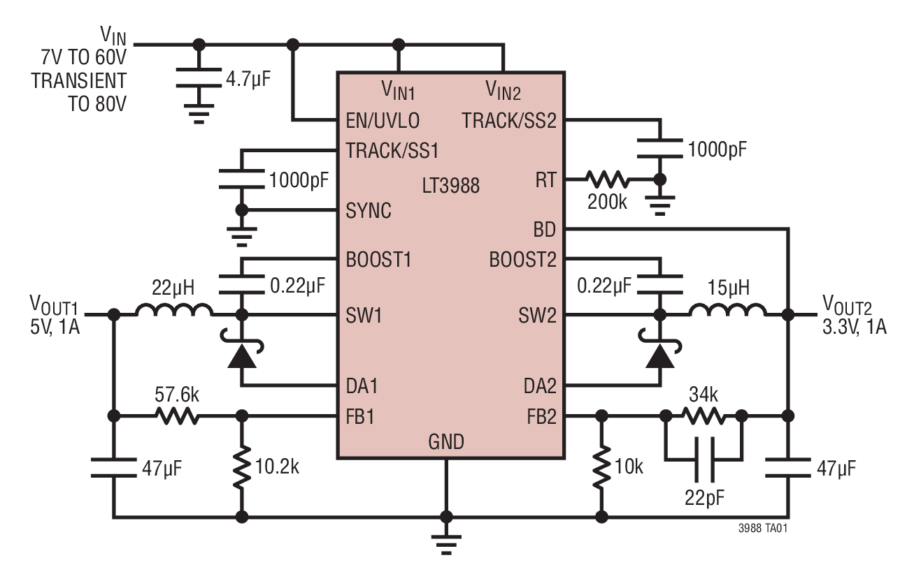
LT3988EMSE Demo Board I 7V ≤ VIN ≤60V, VOUT1 = 5V @ 1A, VOUT2 = 3.3V @ 1A
Analog Devices Inc.Demonstration circuit 1677A is a dual 60V monolithic 1A step-down regulator featuring the LT3988. The demo board operates from inputs up to 60V. The outputs are 5V, 1A and 3.3V,…

LT1999-10 (MS8) Demoboard
Analog Devices Inc.DC1698A-A: Demo Board for the LT1999 High Voltage, Bidirectional Current Sense Amplifier.

LT6108-1 | High Side Current Sense Amplifier with Reference and Comparator
Analog Devices Inc.DC1699A-A: Demo Board for the LT6108 High Side Current Sense Amplifier with Reference and Comparator.
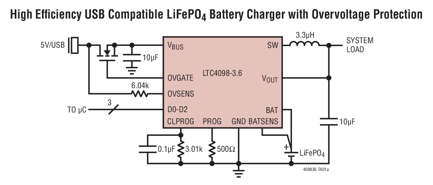
LTC4098-3.6 with HV Buck Regulator Plug in Interface
Analog Devices Inc.DC1701A: Demo Board for the LTC4098/LTC4098-1 USB Compatible Switching Power Managers/Li-Ion Chargers with Overvoltage Protection.

LTC2655-L16 Demo Board | Quad I2C 16-Bit Voltage Output DAC with 1.25V Reference, Requires DC2026
Analog Devices Inc.Demonstration circuit 1703A features the LTC2655 quad 16-/12-bit DAC. The LTC2655 is a family of 16-/12-bit rail-to-rail DACs with integrated 10ppm/°C maximum reference. The…
DC1703A-B
Analog Devices Inc.The LTC2655 is a family of Quad I2C 16-/12-Bit Rail-to-Rail DACs with integrated 10ppm/?C max reference. The DACs have built-in high performance, rail-to-rail, output buffers and…

LTC5590 | Dual 600MHz to 1.7GHz High Dynamic Range Down Mixer Demo Circuit, IF=190MHz, +/-30MHz BW.
Analog Devices Inc.DC1710A-A: Demo Board for the LTC5590 Dual 600MHz to 1.7GHz High Dynamic Range Downconverting Mixer.

LTC4417CUF Demoboard : Prioritized PowerPath Controller
Analog Devices Inc.DC1717A: Demo Board for the LTC4417 Prioritized PowerPath Controller.

DC1719A
Analog Devices Inc.The LTC5569 dual active downconverting mixer is optimized for diversity and MIMO receiver applications that require low power and small size. Each mixer includes an independent LO…

LTC4000EGN/LTC3789EGN Demo Board u 14.6V, 5A Battery Charger with 6VIN to 36VIN Buck-Boost Converter
Analog Devices Inc.DC1721A Demo Board for:
LTC4000 High Voltage High Current Controller for Battery Charging and Power Management
LTC3789 High Efficiency, Synchronous, 4-Switch. Buck-Boost Controller

LT3975 Demo Board I 4.3V ≤ VIN ≤ 42V; VOUT = 3.3V @ 2.5A
Analog Devices Inc.Demonstration circuit 1736A is a monolithic step-down DC/DC switching regulator featuring the LT3975. The demo circuit is designed for 3.3V, 2.5A output from a 4.3V to 42V input.

DC1740A-B
Analog Devices Inc.The LTC3880/LTC3880-1 are dual, PolyPhase DC/DC synchronous step-down switching regulator controllers with an I2C-based PMBus compliant serial interface. The controllers use a…

LTC4370CDE Demo Board | Two-Supply Diode-OR Current Sharing Controller
Analog Devices Inc.DC1741B: Demo Board for the LTC4370 Two-Supply Diode-OR Current Balancing Controller.

LTM2881-3 Low EMI Test Board (For EMI Evaluation Purposes Only, No VL & No GPIO)
Analog Devices Inc.DC1746A-A: Demo Board for LTM2881 Complete Isolated RS485/RS422 µModule Transceiver + Power.

LTM2882-5 Low EMI Test Board (For EMI Evaluation Purposes Only, No VL & No GPIO)
Analog Devices Inc.DC1747A-B: Demo Board for LTM2882 Dual Isolated RS232 µModule Transceiver + Power.

LT8611 Demo Board | Micropower Sync Buck with Current Sense, 3.8V ≤ VIN ≤ 42V, VOUT = 3.3V @ 2.5A
Analog Devices Inc.Demonstration circuit 1750A is a 42V, 2.5A micropower synchronous step-down regulator with current sense featuring the LT8611. The LT8611 is a compact, high efficiency, high speed…

LTM9011-14 Demoboard | 14-Bit, 125Msps, 1.8V Octal Serial ADC, DC < AIN < 70MHz, Requires DC1371 and DC1075
Analog Devices Inc.DC1751A-A: Demo Board for the LTM9011-14 14-Bit, 125Msps Low Power Octal ADCs.

LTC3104EDE Demo Board | 2.5V to 15V input, 3.3V at 300mA (Buck) and 1.8V at 10mA (LDO)
Analog Devices Inc.Demonstration Circuit 1754A features the LTC3104, a high efficiency, monolithic synchronous step-down converter using a current mode architecture capable of supplying 300mA of…

LTC3860EUH Demo Board I VIN Range: 6V to 14V, 1.2V/50A and 1.5V/50A VOUT
Analog Devices Inc.Demonstration circuit DC1755A provides the user with two high current dual phase synchronous buck converters driven by the LTC3860. These buck converters provide outputs of…

LTC2269: 16-bit 20Msps Low Noise ADC, LVDS Outputs, 5-140MHz, Requires DC890, LVDS_XFMR and DC1075
Analog Devices Inc.DC1762A-H: Demo Board for the LTC2269 16-Bit, 20Msps Low Noise ADC.


