Manufacturer
Stock

Displaying 161 - 180 of 5422

Evaluation Kits from Analog Devices Inc.

EVAL-ADM2484EEBZ

Analog Devices Inc.
The ADM2484E is an isolated data transceiver with ?15 kVESD protection suitable for high speed, half- or full-duplex communication on multipoint transmission lines. For half-duplex operation, the transmitter outputs and receiver inputs share the same transmission line. Transmitter Output Pin Y links externally to Receiver Input Pin A, and Transmitter Output Pin Z links externally to Receiver Input Pin B.Designed for balanced transmission lines, the ADM2484Ecomplies with ANSI TIA/EIA RS-485-A-1998 and ISO 8482: 1987(E). The device employs Analog Devices, Inc., iCoupler? technology to combine a 3-channel isolator, a three-state differential line driver, and a differential input receiver into a single package.The differential transmitter outputs and receiver inputs featureelectrostatic discharge circuitry that provides protection up to ?15 kV using the human body model (HBM). The logic side of the device can be powered with either a 5 V or a 3.3 V supply, whereas the bus side requires an isolated 3.3 V supply.The device has current-limiting and thermal shutdown featuresto protect against output short circuits and situations where buscontention causes excessive power dissipation.Applications Isolated RS-485/RS-422 interfaces Industrial field networks INTERBUS Multipoint data transmission systems

EVAL-ADM2485EB5Z

Analog Devices Inc.
The ADM2485 differential bus transceiver is an integrated, galvanically isolated component designed for bidirectional data communication on multipoint bus transmission lines. It is designed for balanced transmission lines and complies with ANSI/TIA/EIA RS-485-A-98 and ISO 8482:1987(E).The device employs Analog Devices, Inc., iCoupler? technology to combine a 3-channel isolator, a three-state differential line driver, and a differential input receiver into a single package. An on-chip oscillator outputs a pair of square waveforms that drive an external transformer to provide isolated power with an external transformer. The logic side of the device can be powered with either a 5 V or a 3.3 V supply, and the bus side is powered with an isolated 5 V supply.The ADM2485 driver has an active high enable. The driver differential outputs and the receiver differential inputs are connected internally to form a differential input/output port that imposes minimal loading on the bus when the driver is disabled or when VDD1 or VDD2 = 0 V. Also provided is an active high receiver disable that causes the receive output to enter a high impedance state.The device has current-limiting and thermal shutdown features to protect against output short circuits and situations where bus contention might cause excessive power dissipation. The part is fully specified over the industrial temperature range and is available in a 16-lead, wide-body SOIC package.Applications Isolated RS-485/RS-422 interfaces PROFIBUS networks Industrial field networks Multipoint data transmission systems

EVAL-ADM2487EEB5Z

Analog Devices Inc.
The ADM2482E/ADM2487E are isolated data transceivers with ?15 kV ESD protection and are suitable for high speed, half-duplex or full-duplex communication on multipoint transmission lines. For half-duplex operation, the transmitter outputs and receiver inputs share the same transmission line. Transmitter Output Pin Y is linked externally to Receiver Input Pin A, and Transmitter Output Pin Z to Receiver Input Pin B. The parts are designed for balanced transmission lines and comply with TIA/EIA- 485-A-98 and ISO 8482:1987(E).The devices employ the Analog Devices, Inc., iCoupler? technology to combine a 3-channel isolator, a three-state differential line driver, and a differential input receiver into a single package. An on-chip oscillator outputs a pair of square waveforms that drive an external transformer to provide isolated power. The logic side of the device can be powered with either a 5 V or a 3.3 V supply, and the bus side is powered with an isolated 3.3 V supply.The ADM2482E/ADM2487E driver has an active high enable, and the receiver has an active low enable. The driver output enters a high impedance state when the driver enable signal is low. The receiver output enters a high impedance state when the receiver enable signal is high.The device has current-limiting and thermal shutdown features to protect against output short circuits and situations where bus contention might cause excessive power dissipation. The part is fully specified over the industrial temperature range of ?40?C to +85?C and is available in a 16-lead, wide-body SOIC package.Applications Isolated RS-485/RS-422 interfaces Industrial field networks Multipoint data transmission systems

EVAL-ADM2687EEBZ

Analog Devices Inc.
The ADM2682E/ADM2687E are fully integrated 5 kV rms signal and power isolated data transceivers with ?15 kV ESD protection and are suitable for high speed communication on multipoint transmission lines. The ADM2682E / ADM2687Einclude an integrated 5 kV rms isolated dc-to-dc power supply that eliminates the need for an external dc-to-dc isolation block.They are designed for balanced transmission lines and comply with ANSI/TIA/EIA-485-A-98 and ISO 8482:1987(E).The devices integrate Analog Devices, Inc., iCoupler? technology to combine a 3-channel isolator, a three-state differential line driver, a differential input receiver, and Analog Devices isoPower? dc-to-dc converter into a single package. The devices are powered by a single 5 V or 3.3 V supply, realizing a fully integrated signal and power isolated RS-485 solution.The ADM2682E/ADM2687E drivers have an active high enable.An active low receiver enable is also provided, which causes thereceiver output to enter a high impedance state when disabled.The devices have current limiting and thermal shutdown features to protect against output short circuits and situations where bus contention may cause excessive power dissipation. The parts are fully specified over the industrial temperature range and are available in a highly integrated, 16-lead, wide-body SOIC package with >8 mm creepage and clearance.The ADM2682E/ADM2687E contain isoPower technology that uses high frequency switching elements to transfer power throughthe transformer. Special care must be taken during printed circuit board (PCB) layout to meet emissions standards. Refer to AN-0971 Application Note, Recommendations for Control of Radiated Emissions with isoPower Devices, for details on board layout considerations.Applications Isolated RS-485/RS-422 interfaces Industrial field networks Multipoint data transmission systems

EVAL-ADM2795EEBZ

Analog Devices Inc.
The ADM2795E is a 5 kV rms signal isolated RS-485 transceiver that features up to ?42 V of ac/dc peak bus overvoltage fault protection on the RS-485 bus pins. The device integrates Analog Devices, Inc., iCoupler? technology to combine a 3-channel isolator, RS-485transceiver, and IEC electromagnetic compatibility (EMC) transient protection in a single package. The ADM2795E is aRS-485/RS-422 transceiver that integrates IEC 61000-4-5 Level 4surge protection, allowing up to ?4 kV protection on the RS-485bus pins (A and B). The device has IEC 61000-4-4 Level 4 EFTprotection up to ?2 kV and IEC 61000-4-2 Level 4 ESD protection on the bus pins, allowing this device to withstand up to ?15 kV on the transceiver interface pins without latching up. This device has an extended common-mode input range of ?25 V to improve data communication reliability in noisy environments. TheADM2795E is capable of operating over wide power supply ranges, with a 1.7 V to 5.5 V VDD1 power supply range, allowing interfacing to low voltage logic supplies. The ADM2795E is also fully TIA/EIA RS-485/RS-422 compliant when operated over a3 V to 5.5 V VDD2 power supply. The device is fully characterizedover an extended operating temperature range of ?40?C to +125?C,and is available in a 16-lead, wide-body SOIC package.Applications Heating, ventilation, and air conditioning (HVAC) networks Industrial field buses Building automation Utility networks

EVAL-ADM2863EEBZ

Analog Devices Inc.
The ADM2861E, ADM2863E, ADM2865E, and ADM2867E are 5.7 kV rms signal and power isolated RS-485 transceivers. These devices are designed for balanced transmission lines and comply with ANSI/TIA/EIA-485-A-98 and ISO 8482:1987(E). The devices pass radiated emissions testing to the EN 55032 Class B standard with margin on a 2-layer printed circuit board (PCB) using two small external 0402 ferrites on isolated power and ground pins. The device features an integrated, low electromagnetic interference (EMI), isolated dc-to-dc converter, which eliminates the need for an external isolated power supply. The isolation barrier provides immunity to system level electromagnetic compatibility (EMC) standards. The family of isolator devices features ?12 kV contact and ?15 kV air IEC61000-4-2 ESD protection on the RS-485 A, B, Y, and Z pins. The devices also features cable invert pins, allowing the user to quickly correct reversed cable connection on the A, B, Y, and Z bus pins while maintaining full receiver fail-safe performance.Slew rate limited versions are available, which are optimized for low speed over long cable runs, and have a maximum data rate of 500 kbps. Half duplex and full duplex variants are available. The full duplex generics allow independent cable inversion of the driver and receiver for additional flexibility.Applications Heating, ventilation, and air conditioning (HVAC) networks Industrial field buses Building automation Utility networks Energy meters

EVAL-ADM3050EEBZ

Analog Devices Inc.
The ADM3050E is a 5.7 kV rms isolated controller area network (CAN) physical layer transceiver with a high performance, basic feature set. The ADM3050E fully meets the CAN flexible data rate (CAN FD) ISO 11898-2:2016 requirements and is further capable of supporting data rates as high as 12 Mbps.The device employs Analog Devices, Inc., iCoupler? technology to combine a 2-channel isolator and a CAN transceiver into a single small outline integrated circuit (SOIC) surface-mount package. The ADM3050E is a fully isolated solution for CAN and CAN FD applications. The ADM3050E provides isolation between the CAN controller and physical layer bus. Safety and regulatory approvals (pending) for a 5.7 kV rms withstand voltage, an 849 VPEAK working voltage, and a 12.8 kV surge test, ensure that the ADM3050E meets application isolation requirements.Low loop propagation delays and the extended common-mode range of ?25 V support robust communication on longer bus cables. Dominant timeout functionality protects against bus lock up in a fault condition, and current limiting and thermal shutdown features protect against output short circuits. The CAN bus input and output pins are protected to ?40 V against accidental connection to a +24 V bus supply. The device is fully specified over the ?40?C to +125?C industrial temperature range.Applications CANOpen, DeviceNet, and other CAN bus implementations Industrial automation Process control and building control Transport and infrastructure

EVAL-ADM3055EEBZ

Analog Devices Inc.
The ADM3055E/ADM3057E are 5 kV rms and 3 kV rms isolated controller area network (CAN) physical layer transceivers with integrated isolated dc-to-dc converters. The ADM3055E/ADM3057E meet flexible data rate (CAN FD) requirements for operation to 5 Mbps and higher and comply with the ISO 11898-2: 2016 standard. The ADM3055E/ADM3057E are capable of supporting data rates as high as 12 Mbps.The devices employ Analog Devices, Inc., iCoupler? technology to combine a 3-channel isolator, a CAN transceiver, and an Analog Devices isoPower? dc-to-dc converter into a single, surface-mount, small outline integrated circuit (SOIC) package. The devices are powered by a single 5 V supply, realizing a fully isolated solution for CAN and CAN FD. Radiated emissions from the high frequency switching of the dc-to-dc convertors are kept below EN 55022 Class B limits by continuous adjustments to the switching frequency.The ADM3055E/ADM3057E provide complete isolation between the CAN controller and physical layer bus. Safety and regulatory approvals (pending) for 5 kV rms isolation voltage, 10 kV surge test, and 8.3 mm creepage and clearance ensure the ADM3055E meets application reinforced isolation requirements. The ADM3057E has an isolation voltage of 3 kV rms and 7.8 mm creepage in a 20-lead, wide body SOIC.Low propagation delays through the isolation support longer bus cables. Slope control mode is available for standard CAN at low data rates. Standby mode minimizes power consumption when the bus is idle or if the node goes offline. Silent mode allows the TXD input to be ignored for listen only mode.Dominant timeout functionality protects against bus lock up in a fault condition. The current limiting and thermal shutdown features protect against output short circuits. The devices are fully specified over an industrial temperature range of ?40?C to +105?C.Applications CANOpen, DeviceNet, and other CAN bus implementations Industrial automation Process control and building control Transport and infrastructure

EVAL-ADM3260MEBZ

Analog Devices Inc.
Based on the iCoupler? and isoPower? chip scale transformertechnology, the ADM3260 is a hot swappable digital and powerisolator with two nonlatching, bidirectional communicationchannels, supporting a complete isolated I2C interface, and anintegrated isolated dc-to-dc converter, supporting up to150 mW of isolated power conversion.iCoupler is a chip scale transformer technology with functional,performance, size, and power consumption advantages ascompared to optocouplers. The bidirectional I2C channels eliminate the need for splitting I2C signals into separate transmitand receive signals for use with standalone optocouplers.Based on the Analog Devices, Inc., isoPower technology, theon-chip isolated dc-to-dc converter provides a regulated, isolatedvoltage of 3.15 V to 5.25 V with up to 150 mW of output power.With the ADM3260, the iCoupler and isoPower channels, alongwith the I2C transceivers, can be integrated with semiconductorcircuitry, which enables a complete isolated I2C interface andallows the power converter to be implemented in a small formfactor. The ADM3260 is available in 20-lead SSOP package andhas an operating temperature range of ?40?C to+105?C.isoPower uses high frequency switching elements to transfer powerthrough its transformer. Special care must be taken during printedcircuit board (PCB) layout to meet emissions standards. See theAN-0971 Application Note for board layout recommendationsApplications Isolated I2C, SMBus, and PMBus interfaces Multilevel I2C interfaces Central office switching Telecommunication and data communication equipment ?48 V distributed power systems ?48 V power supply modules Networking

EVAL-ADN2850SDZ

Analog Devices Inc.
The ADN2850 is a dual-channel, nonvolatile memory, digitallycontrolled resistors?with 1024-step resolution, offeringguaranteed maximum low resistor tolerance error of ?8%. Thedevice performs the same electronic adjustment function as amechanical rheostat with enhanced resolution, solid statereliability, and superior low temperature coefficientperformance. The versatile programming of the ADN2850 viaan SPI?-compatible serial interface allows 16 modes ofoperation and adjustment including scratchpad programming,memory storing and restoring, increment/decrement, ?6 dB/steplog taper adjustment, wiper setting readback, and extra EEMEM?for user-defined information such as memory data for other components, look-up table, or system identificationinformation.In the scratchpad programming mode, a specific setting canbe programmed directly to the RDAC?register, which sets theresistance between Terminal W and Terminal B. This setting canbe stored into the EEMEM and is restored automatically to theRDAC register during system power-on.The EEMEM content can be restored dynamically or throughexternal PR strobing, and a WP function protects EEMEM contents. To simplify the programming, the independent orsimultaneous linear-step increment or decrement commandscan be used to move the RDAC wiper up or down, one step at atime. For logarithmic ?6 dB changes in the wiper setting, theleft or right bit shift command can be used to double or halve theRDAC wiper setting.The ADN2850 patterned resistance tolerance is stored in theEEMEM. The actual full scale resistance can, therefore, beknown by the host processor in readback mode. The host canexecute the appropriate resistance step through a softwareroutine that simplifies open-loop applications as well asprecision calibration and tolerance matching applications.The ADN2850 is available in the 5 mm ? 5 mm 16-lead framechip scale LFCSP and thin, 16-lead TSSOP package. The part isguaranteed to operate over the extended industrial temperaturerange of ?40?C to +85?C.Applications SONET, SDH, ATM, Gigabit Ethernet, DWDM laser diode driver, optical supervisory systems Mechanical rheostat replacement Instrumentation gain adjustment Programmable filters, delays, time constants Sensor calibration

EVAL-ADN4620EBZ

Analog Devices Inc.
The ADN4620/ADN4621 are dual-channel, signal isolated, low voltage differential signaling (LVDS) buffers that operate at up to 2.5 Gbps with very low jitter. The devices integrate Analog Devices, Inc., iCoupler? technology, enhanced for high speed operation to provide drop-in galvanic isolation of LVDS signal chains. AC coupling and/or level shifting to the LVDS receivers and from the LVDS drivers allows isolation of other high speed signals, such as current mode logic (CML).The ADN4620/ADN4621 include a refresh mechanism to monitor the input and output states and ensure that they remain the same in the absence of data transitions (for example, at power-on). For lower power consumption and high speed operation with low jitter, the isolator circuits rely on 1.8 V supplies, while 3.3 V supplies are used for LVDS receivers to support the full common-mode range with an input voltage range (input common mode plus differential input voltage) of 0 V to 2.4 V per Table 2 in the data sheet.The devices are fully specified over a wide industrial temperature range and are available in a compact SSOP package with 5.3 mm creepage (for reinforced insulation at ac mains voltages).APPLICATIONS Analog front-end isolation Data plane isolation Isolated high speed clock and data links Multigigabit serialization/deserialization (SERDES) PCB-to-PCB optical replacement (for example, short reach fiber)Protected by U.S. Patents 7,075,329; 9,941,565; and 10,205,442. Other patents are pending.

EVAL-ADN4624EB1Z

Analog Devices Inc.
The ADN4624 is a quad-channel, signal isolated, low voltage differential signaling (LVDS) buffer that operates at up to 2.5 Gbps with very low jitter. The device integrates Analog Devices, Inc., iCoupler? technology, enhanced for high speed operation to provide drop-in galvanic isolation of LVDS signal chains. AC coupling and/or level shifting to the LVDS receivers and from the LVDS drivers allows isolation of other high speed signals such as current mode logic (CML).The ADN4624 includes a refresh mechanism to monitor the input and output states and ensure they remain the same in the absence of data transitions (for example, at power-on).For lower power consumption and high speed operation with low jitter, the LVDS and isolator circuits rely on 1.8 V supplies. The ADN4624 is fully specified over a wide industrial temperature range and is available in a 28-lead, wide-body, finer pitch SOIC_W_FP package with 8.3 mm creepage and clearance (for 5.7 kV rms or 8 kVPEAK surge and impulse voltages and reinforced insulation at ac mains voltages) or 6 mm ? 6 mm LFCSP package with 1.27 mm creepage and clearance (for basic/functional isolation).APPLICATIONS Isolated video and imaging data Analog front-end isolation Data plane isolation Isolated high speed clock and data links Multi-gigabit serialization/deserialization (SERDES) Board-to-board optical replacement (for example, short reach fiber)

EVAL-ADPD105Z-GEN

Analog Devices Inc.
The ADPD105/ADPD106/ADPD107 are highly efficient,photometric front ends, each with an integrated 14-bit analog-to-digitalconverter (ADC) and a 20-bit burst accumulator thatworks with flexible light emitting diode (LED) drivers. Theaccumulator is designed to stimulate an LED and measurethe corresponding optical return signal. The data output andfunctional configuration occur over a 1.8 V I2C interface on theADPD105 or SPI on the ADPD106 and ADPD107. The controlcircuitry includes flexible LED signaling and synchronousdetection.The analog front end (AFE) features best-in-class rejection of signaloffset and corruption due to modulated interference commonlycaused by ambient light.Couple the ADPD105/ADPD106/ADPD107 with a lowcapacitance photodiode of

EVAL-ADPD6000Z

Analog Devices Inc.
The ADPD6000 is a highly integrated analog front end (AFE) designed for measuring various vital signals.The optical channel is designed as an optical transceiver, stimulating up to four light emitting diodes (LEDs) and measuring the return signal on up to four separate current inputs. The signal chain rejects signal offsets and corruption from asynchronous modulated interference, typically from ambient light, eliminating the need for optical filters or externally controlled dc cancellation circuitry.The electrocardiography (ECG) signal acquisition is designed to support low noise, diagnostic level measurement in the presence of a variety of interferers. The ECG signal chain has a number of complementary features supporting ECG measurement, such as driven reference for common-mode rejection and lead off detection to identify a fallen electrode.The body impedance analysis (BIA) signal chain is designed for body impedance measurement with a configurable excitation path and measurement path. A 12-bit digital-to-analog (DAC) is used in the excitation path to generate the sinusoid wave and high precision measurement, with configurable filters used to measure the body response of the stimulus.The data output and functional configuration use a serial port interface (SPI) on the ADPD6000. The control circuitry includes flexible LED signaling and synchronous detection, digital filters, digital wave generators, and configurable filters.The ADPD6000 is available in a 2.6 mm ? 2.6 mm, 0.4 mm pitch, 36-ball wafer level chip scale package (WLCSP).APPLICATIONS Wearable health and fitness monitors: heart rate, heart rate variability, SpO2, body impedance analysis, hydration, cuffless noninvasive blood pressure Home patient monitoring Industrial monitoring: particle and aerosol, gas, and conductivity detection

EVAL-ADT7310MBZ

Analog Devices Inc.
The ADT7310 is a high accuracy digital temperature sensor in a narrow SOIC package. It contains a band gap temperature reference and a 13-bit ADC to monitor and digitize the temperature to a 0.0625?C resolution. The ADC resolution, by default, is set to 13 bits (0.0625 ?C). This can be changed to 16 bits (0.0078 ?C) by setting Bit 7 in the configuration register (Register Address 0x01).The ADT7310 is guaranteed to operate over supply voltages from 2.7 V to 5.5 V. Operating at 3.3 V, the average supply current is typically 210 ?A. The ADT7310 has a shutdown mode that powers down the device and offers a shutdown current of typically 2 ?A. The ADT7310 is rated for operation over the ?55?C to +150?C temperature range.The CT pin is an open-drain output that becomes active when the temperature exceeds a programmable critical temperature limit. The default critical temperature limit is 147?C. The INT pin is also an open-drain output that becomes active when the temperature exceeds a programmable limit. The INT and CT pins can operate in either comparator or interrupt mode.APPLICATIONS Medical equipment Environmental control systems Computer thermal monitoring Thermal protection Industrial process control Power system monitors Hand-held applications

EVAL-ADT7422MBZ

Analog Devices Inc.
The ADT7422 is a high accuracy, digital I2C temperature sensor?designed to meet the clinical thermometry specification of the?ASTM E1112 standards when soldered onto the final printed?circuit board (PCB).The ADT7422 contains an internal band gap reference, a?temperature sensor, and a precision analog-to-digital converter?(ADC). The ADT7422 provides a 16-bit temperature result?with a resolution of 0.0078?C and an accuracy of up to ?0.1?C?across the temperature range of 25?C to 50?C without the need?for calibration after the PCB soldering process.Operating at 3.0 V, the average supply current is typically 210 ?A.?The ADT7422 has a shutdown mode that powers down the?device and offers a shutdown current of typically 2.0 ?A at 3.0 V.?The ADT7422 is rated for operation over the ?40?C to +125?C?temperature range.Pin A0 and Pin A1 are available for address selection and provide?four possible I2C addresses for the ADT7422. The CT pin is an?open-drain output that becomes active when the temperature?exceeds a programmable critical temperature limit. The INT pin is?also an open-drain output that becomes active when the?temperature exceeds a programmable limit. The INT pin and?CT pin can operate in comparator and interrupt event modes.Product Highlights No calibration or correction required by the user. Low power consumption. Long-term stability and reliability. High accuracy for industrial, instrumentation, and medical applications.Applications Vital signs monitoring (VSM) Medical equipment Resistance temperature detector (RTD) and thermistor replacement Food transportation and storage Thermocouple cold junction compensation Environmental monitoring and heating, ventilation, and air conditioning (HVAC) Laser diode temperature control

EVAL-ADUC7124QSPZ

Analog Devices Inc.
The ADuC7124?is a fully integrated, 1 MSPS, 12-bit data acquisition system incorporating high performance multichannel ADCs, 16-bit/32-bit MCUs, and Flash/EE memory on a single chip.The ADC consists of up to 12 single-ended inputs. An additional two inputs are available but are multiplexed with the two DAC output pins. The ADC can operate in single-ended or differential input mode. The ADC input voltage range is 0 V to VREF. A low drift band gap reference, temperature sensor, and voltage comparator complete the ADC peripheral set.The DAC output range is programmable to one of three voltage ranges. The DAC outputs have an enhanced feature of being able to retain their output voltage during a watchdog or software reset sequence.The device operates from an on-chip oscillator and a PLL generating an internal high frequency clock of 41.78 MHz. This clock is routed through a programmable clock divider from which the MCU core clock operating frequency is generated. The microcontroller core is an ARM7TDMI?, 16-bit/32-bit RISC machine, which offers up to 41 MIPS of peak performance. Thirty-two kilobytes of SRAM and 126 kB of nonvolatile Flash/EE memory are provided on-chip. The ARM7TDMI core views all memory and registers as a single linear array.The ADuC7124 contains an advanced interrupt controller. The vectored interrupt controller (VIC) allows every interrupt to be assigned a priority level. It also supports nested interrupts to a maximum level of eight per IRQ and FIQ. When IRQ and FIQ interrupt sources are combined, a total of 16 nested interrupt levels are supported.On-chip factory firmware supports in-circuit download via the UART serial interface port or the I2C port, while nonintrusive emulation is also supported via the JTAG interface. These features are incorporated into a low cost QuickStart? development system supporting this MicroConverter? family.The part contains a 16-bit PWM with six output signals.For communication purposes, the part contains 2? I2C channels that can be individually configured for master or slave mode. An SPI interface supporting both master and slave modes is also provided. Thirdly, 2? UART channels are provided. Each UART contains a configurable 16-bit FIFO with receive and transmit buffers.The part operates from 2.7 V to 3.6 V and is specified over an industrial temperature range of ?40?C to +125?C. When operating at 41.78 MHz, the power dissipation is typically 120 mW. The ADuC7124 is available in a 64-lead LFCSP package.APPLICATIONS Industrial control and automation systems Smart sensors, precision instrumentation Base station systems, optical networking Patient monitoring

EVAL-ADUC847QSZ

Analog Devices Inc.
The ADuC845, ADuC847, and ADuC848 are single-cycle,12.58 MIPs, 8052 core upgrades to the ADuC834 andADuC836. They include additional analog inputs forapplications requiring more ADC channels.The ADuC845, ADuC847, and ADuC848 are complete smarttransducer front ends. The family integrates high resolution?-? ADCs with flexible, up to 10-channel, input multiplexing, afast 8-bit MCU, and program and data Flash/EE memory on asingle chip.The ADuC845 includes two (primary and auxiliary) 24-bit ?-?ADCs with internal buffering and PGA on the primary ADC.The ADuC847 includes the same primary ADC as the ADuC845(auxiliary ADC removed). The ADuC848 is a 16-bit ADCversion of the ADuC847.The ADCs incorporate flexible input multiplexing, a temperaturesensor (ADuC845 only), and a PGA (primary ADC only)allowing direct measurement of low-level signals. The ADCsinclude on-chip digital filtering and programmable output datarates that are intended for measuring wide dynamic range andlow frequency signals, such as those in weigh scale, strain gage,pressure transducer, or temperature measurement applications.The devices operate from a 32 kHz crystal with an on-chip PLLgenerating a high frequency clock of 12.58 MHz. This clock isrouted through a programmable clock divider from which theMCU core clock operating frequency is generated. The microcontrollercore is an optimized single-cycle 8052 offering up to12.58 MIPs performance while maintaining 8051 instruction setcompatibility.The available nonvolatile Flash/EE program memory optionsare 62 kbytes, 32 kbytes, and 8 kbytes. 4 kbytes of nonvolatileFlash/EE data memory and 2304 bytes of data RAM are alsoprovided on-chip. The program memory can be configured asdata memory to give up to 60 kbytes of NV data memory indata logging applications.On-chip factory firmware supports in-circuit serial downloadand debug modes (via UART), as well as single-pin emulationmode via the EA pin. The ADuC845, ADuC847, and ADuC848are supported by the QuickStart? development system featuringlow cost software and hardware development tools.Applications Multichannel sensor monitoring Industrial/environmental instrumentation Weigh scales, pressure sensors, temperature monitoring Portable instrumentation, battery-powered systems Data logging, precision system monitoring

EVAL-ADUCM410QSPZ

Analog Devices Inc.
The ADuCM410 is a fully integrated, single package device that includes high performance analog peripherals together with digital peripherals (controlled by a 160 MHz Arm? Cortex?-M33 processor) and integrated flash for code and data.The analog-to-digital converter (ADC) on the ADuCM410 provides 16-bit, 2 MSPS data acquisition using up to 16 input pins that can be programmed for single-ended or differential operation with a programmable gain amplifier (PGA) or transimpedance amplifier (TIA) for voltage and current measurements. Additionally, the die temperature and supply voltages can be measured.The ADC input voltage is 0 V to VREF. A sequencer is provided that allows a user to select a set of ADC channels to be measured in sequence without software involvement during the sequence. The sequence can optionally repeat automatically at a user-selectable rate.Up to 12 channels of 12-bit voltage digital-to-analog converters (VDACs) are provided with output buffers supported.The ADuCM410 can be configured so that the digital and analog outputs retain their output voltages through a watchdog or software reset sequence. Therefore, a product can remain functional even while the ADuCM410 is resetting itself.The ADuCM410 has a low power Arm Cortex-M33 processor and a 32-bit reduced instruction set computer (RISC) machine that offers up to 240 MIPS peak performance with a floating-point unit (FPU). Also integrated are 2? 512 kB Flash/EE memories and 128 kB static random access memory (SRAM)?both with single-error correction (SEC) and double error detection (DED) error checking and correction (ECC). The flash comprises two separate 512 kB blocks supporting execution from one flash block and simultaneous writing and/or erasing of the other flash block.The ADuCM410 operates from an on-chip oscillator and has a phase-locked loop (PLL) of 160 MHz. This clock can optionally be divided down to reduce current consumption. Additional low power modes can be set via the ADuCM410 software.The device includes a management data input/output (MDIO) interface capable of operating up to 10 MHz. User programming is eased by incorporating physical address (PHYADR) and device address (DEVAD) hardware comparators. The nonerasable kernel code combined with flags in user flash allow user code to reliably switch between the two hardware independent flash blocks.The ADuCM410 integrates a range of on-chip peripherals that can be configured under software control, as required in the application. These peripherals include 2? universal asynchronous receiver transmitter (UART), 3? I2C, and 3? serial peripheral interface (SPI) serial input/output communication controllers, general-purpose inputs/outputs (GPIOs), 32-element programmable logic arrays (PLAs), five general-purpose timers, a wake-up timer (WUT), and a system watchdog timer (WDT). A 16-bit pulse-width modulation (PWM) with eight output channels is also provided.The GPIO pins (Px.x) power up in high impedance input mode. In output mode, the software chooses between open-drain mode and push/pull mode. The pull-up and pull-down resistors can be disabled and enabled in the software. The GPIO pins can be configured with different voltage levels according to the IOVDDx pin, such as 3.3 V, 1.8 V, and 1.2 V. In GPIO output mode, the inputs can remain enabled to monitor the GPIO pins. The GPIO pins can also be programmed to handle digital or analog peripheral signals, in which case, the pin characteristics are matched to the specific requirement.A large support ecosystem is available for the Arm Cortex-M33 processor to ease product development of the ADuCM410. Access is via the Arm serial wire debug port. On-chip factory firmware supports in-circuit serial download via MDIO or I2C. These features are incorporated into a low cost, quick start development system supporting this precision analog microcontroller.Note that throughout this data sheet, multifunction pins, such as VDAC7/P4.2, are referred to either by the entire pin name or by a single function of the pin, for example, P4.2, when only that function is relevant.APPLICATIONS Optical networking 100 Gbps/200 Gbps/400 Gbps and higher frequency modules Industrial control, automation, and instrumentation systems

EVAL-ADUM3166EBZ

Analog Devices Inc.
The ADuM3165/ADuM31661 are USB 2.0 port isolators, utilizing Analog Devices, Inc., iCoupler? technology to dynamically support all USB 2.0 data rates: low (1.5 Mbps), full (12 Mbps), or high (480 Mbps), as required. The devices support host isolation with automatic speed negotiation as well as peripheral isolation.High speed data is retimed for jitter reduction, requiring an external clock signal or crystal input. The ADuM3165 supports the clock or crystal input on the upstream side, and the ADuM3166 supports the clock or crystal input on the downstream side, offering two options to best suit the system design.The low power standby mode for downstream (Side 2) supports applications with limited available power, such as battery-operated peripherals. The upstream (Side 1) standby current meets USB 2.0 requirements for suspended operation.The isolators are specified over an extended industrial temperature range of ?55?C to +125?C and are available in a compact 20-lead shrink small outline package (SSOP) with 5.3 mm creepage and clearance.APPLICATIONS USB peripheral, USB host, and USB hub isolation Electronic test and measurement equipment Medical devices and integrated PCs Industrial PCs and isolated USB ports for debug or upgrade USB isolator modules and USB cable isolators1 Protected by U.S. Patents 5,952,849; 6,873,065; 6,903,578; and 7,075,329. Other patents are pending.

Displaying 161 - 180 of 5422

Latest Parts

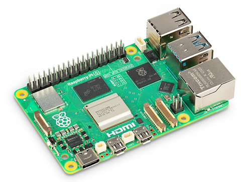
SC1112

Raspberry Pi

$79.61 - $86.40

IN STOCK 10293
Buy

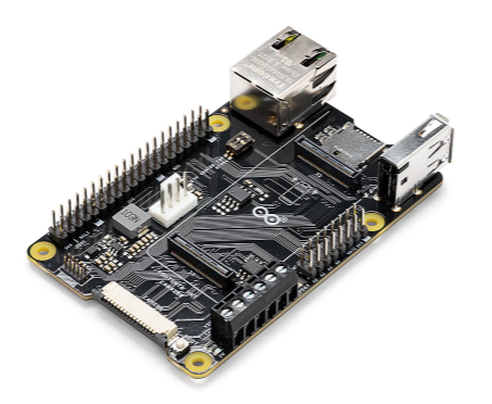
ASX00049

Arduino

* $39.41 - * $44.41

IN STOCK 3132
Buy

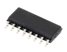
AD96685BRZ

Analog Devices Inc.

$1.72 - * $11.79

IN STOCK 4921
Buy

Reference Designs

RD006

Wurth Elektronik

RD006 - 3 W Dual-output isolated auxiliary supply for communication interfaces and measurement systems

CN0583

Analog Devices Inc.

Multistandard Micropower Verified Smoke Detection System-on-Module

Technical Resources

EVALUATION KITS

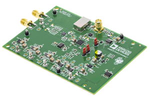
EVAL-AD7124-8SDZ

Analog Devices Inc.

$71.02 - * $75.98

IN STOCK 808
Buy
View All