Manufacturer
Stock

Displaying 201 - 220 of 93388

Parts from Analog Devices Inc.

AD8639WARZ-RL

Part Number : AD8639WARZ-RL

Analog Devices Inc.
The AD8638/AD8639 are single and dual wide bandwidth, auto-zero amplifiers featuring rail-to-rail output swing and low noise. These amplifiers have very low offset, drift, and bias current. Operation is fully specified from 5 V to 16 V single supply (±2.5 V to ±8 V dual supply).The AD8638/AD8639 provide benefits previously found only in expensive zero-drift or chopper-stabilized amplifiers. Using the Analog Devices, Inc., topology, these auto-zero amplifiers combine low cost with high accuracy and low noise. No external capacitors are required. In addition, the AD8638/AD8639 greatly reduce the digital switching noise found in most chopper- stabilized amplifiers.With a typical offset voltage of only 3 μV, drift of 0.01 μV/°C, and noise of 1.2 μV p-p (0.1 Hz to 10 Hz), the AD8638/AD8639 are suited for applications in which error sources cannot be tolerated. Position and pressure sensors, medical equipment, and strain gage amplifiers benefit greatly from nearly zero drift over their operating temperature ranges. Many systems can take advantage of the rail-to-rail output swing provided by the AD8638/AD8639 to maximize signal-to-noise ratio (SNR).The AD8638/AD8639 are specified for the extended industrial temperature range (−40°C to +125°C). The single AD8638 is available in tiny 5-lead SOT-23 and 8-lead SOIC packages. The dual AD8639 is available in 8-lead MSOP, 8-lead SOIC, and 8-lead LFCSP packages.The AD8638/AD8639 are members of a growing series of auto- zero op amps offered by Analog Devices (see Table 1 in the data sheet).ApplicationsPressure and position sensorsStrain gage amplifiers Medical instrumentationThermocouple amplifiers Automotive sensorsPrecision referencesPrecision current sensing

AD8646ARZ

Part Number : AD8646ARZ

Analog Devices Inc.
The AD8646 and the AD8647 are the dual, and the AD8648 isthe quad, rail-to-rail, input and output, single-supply amplifiersfeaturing low offset voltage, wide signal bandwidth, low inputvoltage, and low current noise. The AD8647 also has a lowpower shutdown function.The combination of 24 MHz bandwidth, low offset, low noise,and very low input bias current makes these amplifiers useful ina wide variety of applications. Filters, integrators, photodiodeamplifiers, and high impedance sensors all benefit from thecombination of performance features. AC applications benefitfrom the wide bandwidth and low distortion. The AD8646/AD8647/AD8648 offer high output drive capability, which isexcellent for audio line drivers and other low impedanceapplications. The AD8646 and AD8648 are available forautomotive applications (see the Ordering Guide).Applications include portable and low powered instrumentation,audio amplification for portable devices, portable phoneheadsets, barcode scanners, and multipole filters. The ability toswing rail to rail at both the input and output enables designersto buffer CMOS ADCs, DACs, ASICs, and other wide outputswing devices in single-supply systems.Applications Battery-powered instruments Multipole filters ADC front ends Sensors Barcode scanners ASIC input or output amplifiers Audio amplifiers Photodiode amplifiers Datapath/mux/switch control

AD8667ARMZ

Part Number : AD8667ARMZ

Analog Devices Inc.
The AD8663 / AD8667 / AD8669 are rail-to-rail output amplifiersthat use the Analog Devices, Inc., patented DigiTrim® trimmingtechnique to achieve low offset voltage. The AD8663 / AD8667 /AD8669 feature an extended operating range with supplyvoltages up to 16 V. They also feature low input bias current,low input offset voltage, and low current noise.The combination of low offset, very low input bias current, anda wide supply range makes these amplifiers useful in a wide varietyof applications usually associated with higher priced JFET amplifiers.Systems using high impedance sensors, such as photodiodes,benefit from the combination of low input bias current, lownoise, low offset, and wide bandwidth.The ability to operate the device for single (5 V to 16 V) or dualsupplies (±2.5 V to ±8 V) supports many applications. The railto-railoutputs provide increased dynamic range to drive lowfrequency data converters. The low bias current drift is wellsuitedfor precision I-to-V converters. The combination ofprecision offset, offset drift, and low noise also make the opamps ideal for gain, dc offset adjust, and active filter in bothinstrumentation and medical applications. These low powerop amps can be used in IR thermometers, pH and ORP instruments,pressure transducer front ends, and other sensor signalconditioning circuits that are used in remote or wirelessapplications.The AD8663 / AD8667 / AD8669 are specified over the extendedindustrial temperature range of −40°C to +125°C. The singleAD8663 is available in a narrow 8-lead SOIC package and a verythin, 8-lead LFCSP. The dual AD8667 is available in a narrow8-lead SOIC package and an 8-lead MSOP. The quad AD8669is available in a 14-lead SOIC and 14-lead small TSSOP. Applications Sensor front ends Transimpedance amplifiers Electrometer applications Photodiode amplification Low power ADC drivers Medical diagnostic instruments pH and ORP meters and probes DAC or REF buffers

AD8675ARMZ

Part Number : AD8675ARMZ

Analog Devices Inc.
The AD8675 precision operational amplifier has ultralow offset, drift, and voltage noise combined with very low input bias currents over the full operating temperature range. The AD8675 is a precision, wide bandwidth op amp featuring rail-to-rail output swings and very low noise. Operation is fully specified from ±5 V to ±15 V.The AD8675 features a rail-to-rail output like that of the OP184, but with wide bandwidth and even lower voltage noise, com-bined with the precision and low power consumption like that of the industry-standard OP07 amplifier. Unlike other low noise, rail-to-rail op amps, the AD8675 has very low input bias current and low input current noise.With typical offset voltage of only 10 μV, offset drift of 0.2 μV/°C, and noise of only 0.10 μV p-p (0.1 Hz to 10 Hz), the AD8675 is perfectly suited for applications where large error sources cannot be tolerated. For applications with even lower offset tolerances, the proprietary nulling capability allows a combination of both device and system offset errors up to 3.5 mV (referred to the input) to be compensated externally. Unlike previous circuits, the AD8675 accommodates this adjustment without adversely affecting the offset drift, CMRR, and PSRR of the amplifier. Precision instrumentation, PLL, and other precision filter circuits, position and pressure sensors, medical instrumentation, and strain gage amplifiers benefit greatly from the very low noise, low input bias current, and wide bandwidth. Many systems can take advantage of the low noise, dc precision, and rail-to-rail output swing provided by the AD8675 to maximize SNR and dynamic range.The smaller packages and low power consumption afforded by the AD8675 allow maximum channel density or minimum board size for space-critical equipment.The AD8675 is specified for the extended industrial temperature range (−40°C to +125°C). The AD8675 amplifier is available in the tiny 8-lead MSOP, and the popular 8-lead, narrow SOIC, RoHS compliant packages. MSOP packaged devices are only available in tape and reel format.Applications Precision instrumentation PLL filters Laser diode control loops Strain gage amplifiers Medical instrumentation Thermocouple amplifiers

AD8682ARZ

Part Number : AD8682ARZ

Analog Devices Inc.
The AD8682 and AD8684 are dual and quad low power, precision (1 mV) JFET amplifiers featuring excellent speed at low supply currents. The slew rate is typically 9 V/μs with a supply current under 250 μA per amplifier. These unity-gain stable amplifiers have a typical gain bandwidth of 3.5 MHz. The JFET input stage ensures bias current is typically a few picoamps and below 125 pA maximum over the full temperature operating range.The devices are ideal for portable, low power applications, especially with high source impedance. The devices are unity gain stable and can drive higher capacity loads (G = 1, noninverting), as an example of their excellent dynamic response over a wide range of conditions, delivering dc precision performance at low quiescent currents.Applications Portable telecommunications Low power industrial and instrumentation Loop filters Active and precision filters Integrators Strain gauge amplifiers Portable medical instrumentation Supply current monitoring

AD8694ARUZ

Part Number : AD8694ARUZ

Analog Devices Inc.
The AD8691, AD8692, and AD8694 are low cost, single, dual, and quad rail-to-rail output, single-supply amplifiers featuring low offset and input voltages, low current noise, and wide signal bandwidth. The combination of low offset, low noise, very low input bias currents, and high speed make these amplifiers useful in a wide variety of applications. Filters, integrators, photodiode amplifiers, and high impedance sensors all benefit from this combination of performance features. Audio and other ac applications benefit from the wide bandwidth and low distortion of these devices.Applications for these amplifiers include power amplifier (PA) controls, laser diode control loops, portable and loop-powered instrumentation, audio amplification for portable devices, and ASIC input and output amplifiers.The small SC70 and TSOT package options for the AD8691 allow it to be placed next to sensors, thereby reducing external noise pickup.The AD8691, AD8692, and AD8694 are specified over the extended industrial temperature range of −40°C to +125°C. The AD8691 single is available in 5-lead SC70 and 5-lead TSOT packages. The AD8692 dual is available in 8-lead MSOP and narrow SOIC surface-mount packages. The AD8694 quad is available in 14-lead TSSOP and narrow 14-lead SOIC packages.See ordering guide section for automotive grades.Applications Photodiode amplification Battery-powered instrumentation Medical instruments Multipole filters Sensors Portable audio devices

AD9215BRUZ-65

Part Number : AD9215BRUZ-65

Analog Devices Inc.
The AD9215 is a family of monolithic, single 3 V supply, 10-bit, 65/80/105 MSPS analog-to-digital converters (ADC). This family features a high performance sample-and-hold amplifier (SHA) and voltage reference. The AD9215 uses a multistage differential pipelined architecture with output error correction logic to provide 10-bit accuracy at 105 MSPS data rates and to guarantee no missing codes over the full operating temperature range.The wide bandwidth, truly differential sample-and-hold amplifier (SHA) allows for a variety of user-selectable input ranges and offsets including single-ended applications. It is suitable for multiplexed systems that switch full-scale voltage levels in successive channels and for sampling single-channel inputs at frequencies well beyond the Nyquist rate. Combined with power and cost savings over previously available ADCs, the AD9215 is suitable for applications in communications, imaging, and medical ultrasound.A single-ended clock input is used to control all internal conversion cycles. A duty cycle stabilizer compensates for wide variations in the clock duty cycle while maintaining excellent performance. The digital output data is presented in straight binary or twos complement formats. An out-of-range signal indicates an overflow condition, which can be used with the MSB to determine low or high overflow.Fabricated on an advanced CMOS process, the AD9215 is available in both a 28-lead surface-mount plastic package and a 32-lead chip scale package and is specified over the industrial temperature range of −40°C to +85°C.PRODUCT HIGHLIGHTS The AD9215 operates from a single 3 V power supply and features a separate digital output driver supply to accommodate 2.5 V and 3.3 V logic families. Operating at 105 MSPS, the AD9215 core ADC consumes a low 120 mW; at 80 MSPS, the power dissipation is 104 mW; and at 65 MSPS, the power dissipation is 96 mW. The patented SHA input maintains excellent performance for input frequencies up to 200 MHz and can be configured for single-ended or differential operation. The AD9215 is part of several pin compatible 10-, 12-, and 14-bit low power ADCs. This allows a simplified upgrade from 10 bits to 12 bits for systems up to 80 MSPS. The clock duty cycle stabilizer maintains converter performance over a wide range of clock pulse widths. The out of range (OR) output bit indicates when the signal is beyond the selected input range.APPLICATIONS Ultrasound equipment IF sampling in communications receivers Battery-powered instruments Hand-held scopemeters Low cost digital oscilloscopes

AD9229ABCPZ-50

Part Number : AD9229ABCPZ-50

Analog Devices Inc.
The AD9229 is a 50 or 65 MSPS quad 12-bit, analog–to–digital converter with serial LVDS outputs. An on–chip track–and–hold circuit is designed for low cost, low power, small size and ease of use. The product operates up to a 65 MSPS conversion rate and is optimized for outstanding dynamic performance where a small package size is critical.The ADC requires a single +3 V power supply. No external reference or driver components are required for many applications. A separate output power supply pin supports LVDS compatible serial digital output levels.The ADC automatically multiplies up the sample rate clock for the appropriate LVDS serial data rate. This data clock output (DCO) provides operation up to 390 MHz and supports double-data rate operation (DDR). An MSB trigger or Frame clock is also provided to signal a new output byte. Power down is supported, and the ADC consumes 3 mW when enabled.Fabricated on an advanced CMOS process, the AD9229 is available in a 48-pin chip scale 7 mm x 7 mm package (48-LFCSP) specified over the industrial temperature range (–40°C to +85°C).ApplicationsDigital beam forming systems for ultrasound Wireless and wired broadband communications Communication test equipment

AD9778A-DPG2-EBZ

Part Number : AD9778A-DPG2-EBZ

Analog Devices Inc.
The AD9776A/AD9778A/AD9779A are dual, 12-/14-/16-bit, high dynamic range digital-to-analog converters (DACs) that provide a sample rate of 1 GSPS, permitting a multicarrier generation up to the Nyquist frequency. They include features optimized for direct conversion transmission applications, including complex digital modulation and gain and offset compensation. The DAC outputs are optimized to interface seamlessly with analog quadrature modulators such as the ADL537x FMOD series from Analog Devices, Inc. A 3-wire interface provides for programming/readback of many internal parameters. Full-scale output current can be programmed over a range of 10 mA to 30 mA. The devices are manufactured on an advanced 0.18 μm CMOS process and operate on 1.8 V and 3.3 V supplies for a total power consumption of 1.0 W. They are enclosed in a 100-lead thin quad flat package (TQFP).Product Highlights Ultralow noise and intermodulation distortion (IMD) enable high quality synthesis of wideband signals from baseband to high intermediate frequencies. A proprietary DAC output switching technique enhances dynamic performance. The current outputs are easily configured for various single-ended or differential circuit topologies. CMOS data input interface with adjustable setup and hold. Novel 2×, 4×, and 8× interpolator/coarse complex modulator allows carrier placement anywhere in DAC bandwidth.Applications Wireless infrastructure W-CDMA, CDMA2000, TD-SCDMA, WiMax, GSM, LTE Digital high or low IF synthesis Internal digital upconversion capability Transmit diversity Wideband communications: LMDS/MMDS, point-to-point

AD9880KSTZ-150

Part Number : AD9880KSTZ-150

Analog Devices Inc.
The AD9880 offers designers the flexibility of an analog interface and High-Definition Multimedia Interface (HDMI™) receiver integrated on a single chip. Also included is support for High bandwidth Digital Content Protection (HDCP).ANALOG INTERFACEThe AD9880 is a complete 8-bit 150 MSPS monolithic analog interface optimized for capturing Component Video (YPbPr) and RGB graphics signals. Its 150 MSPS encode rate capability and full power analog bandwidth of 300 MHz supports all HDTV formats (up to 1080p) and FPD resolutions up to SXGA (1280 × 1024 at 75 Hz).The analog interface includes a 150 MHz triple ADC with internal 1.25V reference, a Phase Locked Loop (PLL), and programmable gain, offset, and clamp control. The user provides only 1.8V and 3.3V power supply, analog input, and Hsync. Three-state CMOS outputs may be powered from 1.8V to 3.3V. The AD9880’s on-chip PLL generates a pixel clock from Hsync. Pixel clock output frequencies range from 12 MHz to 150 MHz. PLL clock jitter is typically less than 500 ps p-p at 150 MHz. The AD9880 also offers full sync processing for composite sync and Sync-on-Green (SOG) applications.DIGITAL INTERFACEThe AD9880 contains a HDMI v1.1 compatible receiver and supports all HDTV formats (up to 1080p) and display resolutions up to SXGA (1280 × 1024 at 75 Hz). The receiver features an intra-pair skew tolerance of up to one full clock cycle. With the inclusion of HDCP, displays may now receive encrypted video content. The AD9880 allows for authentication of a video receiver, decryption of encoded data at the receiver, and renewability of that authentication during transmission as specified by the HDCP v1.1 protocol.Fabricated in an advanced CMOS process, the AD9880 is provided in a space-saving 100-lead LQFP surface-mount Pb-free plastic package and is specified over the 0 ºC to 70 ºC temperature range.APPLICATIONS Advanced TV HDTV Projectors LCD Monitor

AD9957BSVZ

Part Number : AD9957BSVZ

Analog Devices Inc.
The AD9957 functions as a universal I/Q modulator and agileupconverter for communications systems where cost, size, powerconsumption, and dynamic performance are critical. TheAD9957 integrates a high speed, direct digital synthesizer(DDS), a high performance, high speed, 14-bit digital-to-analogconverter (DAC), clock multiplier circuitry, digital filters, andother DSP functions onto a single chip. It provides basebandupconversion for data transmission in a wired or wirelesscommunications system.The AD9957 is the third offering in a family of quadraturedigital upconverters (QDUCs) that includes the AD9857 andAD9856. It offers performance gains in operating speed, powerconsumption, and spectral performance. Unlike its predecessors,it supports a 16-bit serial input mode for I/Q baseband data.The device can alternatively be programmed to operate either asa single tone, sinusoidal source or as an interpolating DAC.The reference clock input circuitry includes a crystal oscillator,a high speed, divide-by-two input, and a low noise PLL formultiplication of the reference clock frequency.The user interface to the control functions includes a serial porteasily configured to interface to the SPORT of the Blackfin®DSP and profile pins to enable fast and easy shift keying of anysignal parameter (phase, frequency, or amplitude).Applications HFC data, telephony, and video modems Wireless base station transmissions Broadband communications transmissions Internet telephony

ADCMP604BKSZ-R2

Part Number : ADCMP604BKSZ-R2

Analog Devices Inc.
The ADCMP604 / ADCMP605 are very fast comparators fabricated on the Analog Devices, Inc. proprietary XFCB2 process. These comparators are exceptionally versatile and easy to use. Features include an input range from VEE − 0.5 V to VCCI + 0.2 V, low noise, LVDS-compatible output drivers, and TTL/CMOS latch inputs with adjustable hysteresis and/or shut-down inputs.The devices offer 1.5 ns propagation delays with 1 ps rms random jitter (RJ). Overdrive and slew rate dispersion are typically less than 50 ps.A flexible power supply scheme allows the devices to operate with a single 2.5 V positive supply and a −0.5 V to +2.7 V input signal range up to a 5.5 V positive supply with a −0.5 V to +5.7 V input signal range. Split input/output supplies, with no sequencing restrictions on the ADCMP605, support a wide input signal range with greatly reduced power consumption.The LVDS-compatible output stage is designed to drive any standard LVDS input. The comparator input stage offers robust protection against large input overdrive, and the outputs do not phase reverse when the valid input signal range is exceeded. High speed latch and programmable hysteresis features are also provided in a unique single-pin control option.The ADCMP604 is available in a 6-lead SC70 package, and the ADCMP605 is available in a 12-lead LFCSP.APPLICATIONS High speed instrumentation Clock and data signal restoration Logic level shifting or translation Pulse spectroscopy High speed line receivers Threshold detection Peak and zero-crossing detectors High speed trigger circuitry Pulse-width modulators Current-/voltage-controlled oscillators Automatic test equipment (ATE)

ADF4154BCPZ

Part Number : ADF4154BCPZ

Analog Devices Inc.
The ADF4154 is a fractional-N frequency synthesizer that implements local oscillators in the up conversion and down conversion sections of wireless receivers and transmitters. It consists of a low noise digital phase frequency detector (PFD), a precision charge pump, and a programmable reference divider. There is a Σ-Δ based fractional interpolator to allow programmable fractional-N division. The INT, FRAC, and MOD registersdefine an overall N divider (N = (INT + (FRAC/MOD))). In addition, the 4-bit reference counter (R counter) allows selectable REFIN frequencies at the PFD input. A complete phase-locked loop (PLL) can be implemented if the synthesizer is used with an external loop filter and a voltage controlled oscillator (VCO).A key feature of the ADF4154 is the fast-lock mode with a builtintimer. The user can program a predetermined count-down time value so that the PLL will remain in wide bandwidth mode, instead of having to control this time externally.Control of all on-chip registers is via a simple 3-wire interface. The device operates with a power supply ranging from 2.7 V to 3.3 V, and can be powered down when not in use.

ADG1208YRUZ

Part Number : ADG1208YRUZ

Analog Devices Inc.
The ADG1208 and ADG1209 are monolithic, iCMOS® analogmultiplexers comprising eight single channels and four differentialchannels, respectively. The ADG1208 switches one of eight inputsto a common output as determined by the 3-bit binary addresslines A0, A1, and A2. The ADG1209 switches one of fourdifferential inputs to a common differential output as determinedby the 2-bit binary address lines A0 and A1. An EN input onboth devices enable or disable the device. When disabled, allchannels are switched off. When on, each channel conductsequally well in both directions and has an input signal rangethat extends to the supplies.The iCMOS (industrial CMOS) modular manufacturingprocess combines high voltage CMOS (complementary metal-oxidesemiconductor) and bipolar technologies. It enables thedevelopment of a wide range of high performance analog ICscapable of 33 V operation in a footprint that no other generationof high voltage devices has been able to achieve. Unlike analogICs using conventional CMOS processes, iCMOS componentscan tolerate high supply voltages while providing increasedperformance, dramatically lower power consumption, andreduced package size.The ultralow capacitance and exceptionally low charge injectionof these multiplexers make them ideal solutions for data acquisitionand sample-and-hold applications, where low glitch and fastsettling are required. There is minimum chargeinjection over the entire signal range of the device. iCMOSconstruction also ensures ultralow power dissipation, making theds ideally suited for portable and battery-powered instruments.Applications Audio and video routing Automatic test equipment Data-acquisition systems Battery-powered systems Sample-and-hold systems Communication systems

ADG3308BCPZ-REEL7

Part Number : ADG3308BCPZ-REEL7

Analog Devices Inc.
The ADG3308 is a bidirectional level translator containing eight bidirectional channels. The ADG3308 can be used in multivoltage digital system applications, such as a data transfer between a low voltage DSP controller and a higher voltage device. The internal architecture allows the device to perform bidirectional level translation without an additional signal to set the direction in which the translation takes place.The voltage applied to VCCA sets the logic levels on the A side of the device, and VCCY sets the levels on the Y side. For proper operation, VCCA must always be less than VCCY. The VCCA compatible logic signals applied to the A side of the device appear as VCCY compatible levels on the Y side. Similarly, VCCY compatible logic levels applied to the Y side of the device appear as VCCA compatible logic levels on the A side.The enable pin (EN) provides three-state operation on both the A side and the Y side pins. When the EN pin is pulled low, the terminals on both sides of the device are in the high impedance state. For normal operation, EN should be driven high.The ADG3308 is available in a compact 20-lead TSSOP and a 20-lead LFCSP. The EN pin is referred to the VCCY supply voltage. The ADG3308 is guaranteed to operate over the 1.15 V to 5.5 V supply voltage range and the extended −40°C to +85°C temperature range.Product Highlights Bidirectional logic level translation. Fully guaranteed over the 1.15 V to 5.5 V supply range. No direction pin. Packages: 20-lead TSSOP and 20-lead LFCSPApplications Low voltage ASIC level translation Smart card readers Cell phones and cell phone cradles Portable communication devices Telecommunications equipment Network switches and routers Storage systems (SAN/NAS) Computing/server applications GPS Portable POS systems Low cost serial interfaces

ADG601BRTZ-REEL7

Part Number : ADG601BRTZ-REEL7

Analog Devices Inc.
The ADG601 / ADG602 are monolithic, CMOS single-pole single-throw (SPST) switches with on resistance typically less than 2.5 Ω. The low on-resistance flatness makes the ADG601 / ADG602 ideally suited to many applications, particularly those requiring low distortion. These switches are ideal replacements for mechanical relays because they are more reliable, have lower power requirements, and are available in much smaller package sizes.The ADG601 is a normally open (NO) switch, and the ADG602 is a normally closed (NC) switch. Each switch conducts equally well in both directions when the device is on, with the input signal range extending to the supply rails.The switches are available in tiny, 6-lead SOT-23; 8-lead MSOP; and 820 μm × 2255 μm die.PRODUCT HIGHLIGHTS Low on resistance (2 Ω typical) Dual ±2.7 V to ±5.5 V or single +2.7 V to +5.5 V supplies Tiny, 6-lead SOT-23; 8-lead MSOP; and 820 μm × 2255 μm die Rail-to-rail input signal rangeAPPLICATIONS Automatic test equipment Power routing Communication systems Data acquisition systems Sample-and-hold systems Avionics Relay replacement Battery-powered systems

ADG759BCPZ

Part Number : ADG759BCPZ

Analog Devices Inc.
The ADG759 is a low voltage, CMOS analog multiplexer comprising four differential channels. The ADG759 switches one of four differential inputs to a common differential output as determined by the 2-bit binary address lines A0 and A1. An EN input is used to enable or disable the device. When disabled, all channels are switched OFF.Low power consumption and operating supply range of 1.8 V to 5.5 V make the ADG759 ideal for battery-powered, portable instruments. All channels exhibit break-before-make switching action preventing momentary shorting when switching channels.The ADG759 is available in a 16-lead TSSOP package.APPLICATIONS Data Acquisition Systems Communication Systems Relay Replacement Audio and Video Switching Battery-Powered SystemsPRODUCT HIGHLIGHTS Small 20-Lead 4 mm × 4 mm Chip Scale Packages (CSP). Single/Dual Supply Operation. The ADG758 and ADG759 are fully specified and guaranteed with 3 V and 5 V single-supply and ±2.5 V dual-supply rails. Low RON (3 Ω Typical). Low Power Consumption (

ADG819BRTZ-500RL7

Part Number : ADG819BRTZ-500RL7

Analog Devices Inc.
The ADG819 is a monolithic, CMOS SPDT (single pole, double throw) switch. This switch is designed on a submicron process, that provides low power dissipation yet gives high switching speed, low On Resistance and low leakage currents. Low-power consumption and operating supply range of +1.8 V to +5.5 V make the ADG819 ideal for battery-powered, portable instruments.Each switch of the ADG819 conducts equally well in both directions when on. The ADG819 exhibits break-before- make switching action, thus preventing momentary shorting when switching channels. (See the ADG820 for a switch exhibiting make-before-break action.)The ADG819 is available in a 6-lead SOT-23 package and an 8-lead µSOIC package as well as a 2×3 array MicroCSP package. This chip occupies only a 2.18mm × 1.14mm area, thus making it the ideal candidate for space-constrained applications.

ADG854BCPZ-REEL7

Part Number : ADG854BCPZ-REEL7

Analog Devices Inc.
The ADG854 is a low voltage CMOS device containing two independently selectable single-pole, double-throw (SPDT) switches. This device offers ultralow on resistance of less than 0.8 Ω over the full temperature range. The ADG854 is fully specified for 5.5 V, 3.3 V, and 2.5 V supply operation. Each switch conducts equally well in both directions when on, and has an input signal range that extends to the supplies. The ADG854 exhibits break-before-make switching action. The ADG854 is available in a 1.6 mm × 1.3 mm 10-lead mini LFCSP package.Applications Cellular phones PDAs MP3 players Power routing Battery-powered systems PCMCIA cards Modems Audio and video signal routing Communication systems

ADL5387-EVALZ

Part Number : ADL5387-EVALZ

Analog Devices Inc.
The ADL5387 is a broadband quadrature I/Q demodulator that covers an RF/IF input frequency range from 30 MHz to 2 GHz. With a NF = 13.2 dB, IP1dB = 12.7 dBm, and IIP3 = 32 dBm @ 450 MHz, the ADL5387 demodulator offers outstanding dynamic range suitable for the demanding infrastructure direct-conversion requirements. The differential RF/IF inputs provide a well-behaved broadband input impedance of 50 Ω and are best driven from a 1:1 balun for optimum performance.Ultrabroadband operation is achieved with a divide-by-2 method for local oscillator (LO) quadrature generation. Over a wide range of LO levels, excellent demodulation accuracy is achieved with amplitude and phase balances ~0.05 dB and ~0.4°, respectively. The demodulated in-phase (I) and quadrature (Q) differential outputs are fully buffered and provide a voltage conversion gain of >4 dB. The buffered baseband outputs are capable of driving a 2 Vp-p differential signal into 200 Ω.The fully balanced design minimizes effects from second-order distortion. The leakage from the LO port to the RF port is 60 dBm.The ADL5387 operates off a single 4.75 V to 5.25 V supply. The supply current is adjustable with an external resistor from the BIAS pin to ground.The ADL5387 is fabricated using the Analog Devices, Inc. advanced silicon-germanium bipolar process and is available in a 24-lead exposed paddle LFCSP.APPLICATIONS QAM/QPSK RF/IF demodulators W-CDMA/CDMA/CDMA2000/GSM Microwave point-to-(multi)point radios Broadband wireless and WiMAX Broadband CATVs

Displaying 201 - 220 of 93388

Latest Parts

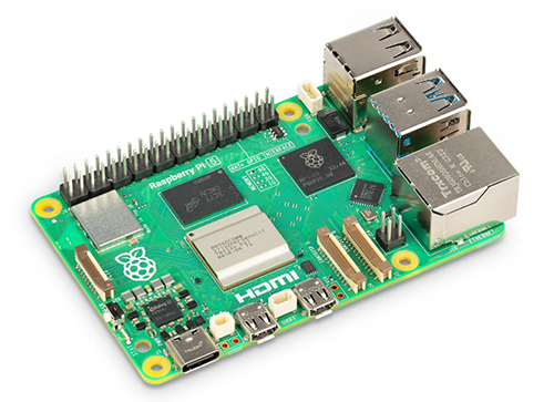
SC1112

Raspberry Pi

$79.61 - $86.40

IN STOCK 10293
Buy

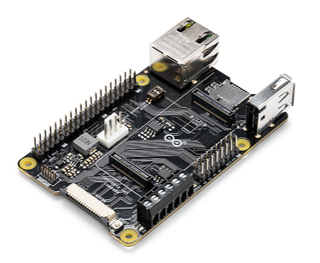
ASX00049

Arduino

* $39.41 - * $44.41

IN STOCK 3132
Buy

AD96685BRZ

Analog Devices Inc.

$1.72 - * $11.79

IN STOCK 4921
Buy

Reference Designs

RD006

Wurth Elektronik

RD006 - 3 W Dual-output isolated auxiliary supply for communication interfaces and measurement systems

CN0583

Analog Devices Inc.

Multistandard Micropower Verified Smoke Detection System-on-Module

Technical Resources

EVALUATION KITS

EVAL-AD7124-8SDZ

Analog Devices Inc.

$71.02 - * $75.98

IN STOCK 808
Buy
View All