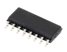
AD5687BRUZ
Part Number : AD5687BRUZ
Analog Devices Inc.The AD5689/AD5687 members of the nanoDAC+™ family arelow power, dual, 16-/12-bit, buffered voltage output digital-to-analogconverters (DACs). The devices include a gain select pingiving a full-scale output of 2.5 V (gain = 1) or 5 V (gain = 2). TheAD5689/AD5687 operate from a single 2.7 V to 5.5 V supply, areguaranteed monotonic by design, and exhibit less than 0.1% FSRgain error and 1.5 mV offset error performance. Both devices areavailable in a 3 mm × 3 mm LFCSP and a TSSOP package.The AD5689/AD5687 also incorporate a power-on reset circuitand a RSTSEL pin that ensure that the DAC outputs power upto zero scale or midscale and remain there until a valid writetakes place. Each part contains a per channel power-down featurethat reduces the current consumption of the device to 4 µA at3 V while in power-down mode.The AD5689/AD5687 uses a versatile serial peripheral interfacethat operates at clock rates up to 50 MHz. Both devices containa VLOGIC pin that is intended for 1.8 V/3 V/5 V logic.Product Highlights High Relative Accuracy (INL). AD5687 (12-bit): ±1 LSB maximum Excellent DC Performance. Total unadjusted error: ±0.1% of FSR maximum Offset error: ±1.5 mV maximum Gain error: ±0.1% of FSR maximum Two Package Options. 3 mm × 3 mm, 16-lead LFCSP or 16-lead TSSOPApplications Optical transceivers Base station power amplifiers Process control (PLC I/O cards) Industrial automation Data acquisition systems
AD5700-1BCPZ-RL7
Part Number : AD5700-1BCPZ-RL7
Analog Devices Inc.The AD5700/AD5700-1 are single-chip solutions, designedand specified to operate as a HART® FSK half-duplex modem,complying with the HART physical layer requirements. TheAD5700/AD5700-1 integrate all of the necessary filtering, signaldetection, modulating, demodulating and signal generationfunctions, thus requiring few external components. The 0.5%precision internal oscillator on the AD5700-1 greatly reducesthe board space requirements, making it ideal for line-poweredapplications in both master and slave configurations. The maximumsupply current consumption is 115µA, making theAD5700/AD5700-1 an optimal choice for low power loop-powered applications.Transmit waveforms are phase continuous 1200 Hz and2200 Hz sinusoids. The AD5700/AD5700-1 contain accuratecarrier detect circuitry and use a standard UART interface.Applications Field transmitters HART multiplexers PLC and DCS analog I/O modules HART network connectivity
AD7176-2BRUZ-RL
Part Number : AD7176-2BRUZ-RL
Analog Devices Inc.The AD7176-2 is a fast settling, highly accurate, high resolution,multiplexed Σ-Δ analog-to-digital converter (ADC) for low bandwidthinput signals. Its inputs can be configured as two fullydifferential or four pseudo differential inputs via the integratedcrosspoint multiplexer. An integrated precision, 2.5 V, low drift(2 ppm/°C), band gap internal reference (with an outputreference buffer) adds functionality and reduces the externalcomponent count.The maximum channel scan data rate is 50 kSPS/channel(settling time of 20 µs), resulting in fully settled data with17 noise free bits. User-selectable output data rates range from5 SPS to 250 kSPS. The resolution increases at lower speeds.The AD7176-2 offers three key digital filters. The fast settlingsinc5 + sinc1 filter maximizes the channel scan rate. The sinc3filter maximizes the resolution for single-channel, low speedapplications. For 50 Hz and 60 Hz environments, the AD7176-2specific filter minimizes the settling times or maximizes therejection of the line frequency. These enhanced filters enablesimultaneous 50 Hz and 60 Hz rejection with a 27 SPS outputdata rate (with a settling time of 36 ms).System offset and gain errors can be corrected on a per channelbasis. This per channel configurability extends to the output datarate used for each channel when using a sinc5 + sinc1 filter. Allswitching of the crosspoint multiplexer is controlled by the ADCand can be configured to automatically control an externalmultiplexer via the GPIO pins.The specified operating temperature range is −40°C to +105°C.The AD7176-2 is housed in a 24-lead TSSOP package.Applications Process control: PLC/DCS modules - Temperature and pressure measurement Medical and scientific multichannel instrumentation Chromatography
AD8417WHRZ
Part Number : AD8417WHRZ
Analog Devices Inc.The AD8417 is a high voltage, high resolution current shunt amplifier. It features an initial gain of 60 V/V, with a maximum ±0.3% gain error over the entire temperature range. The buffered output voltage directly interfaces with any typical converter. The AD8417 offers excellent input common-mode rejection from −2 V to +70 V. The AD8417 performs bidirectional current measurements across a shunt resistor in a variety of automotive and industrial applications, including motor control, power management, and solenoid control.The AD8417 offers breakthrough performance throughout the −40°C to +150°C temperature range. It features a zero drift core, which leads to a typical offset drift of 0.1 µV/°C throughout the operating temperature range and the common-mode voltage range. The AD8417 is qualified for automotive applications. The device includes EMI filters and patented circuitry to enable output accuracy with pulse-width modulation (PWM) type input common-mode voltages. The typical input offset voltage is ±200 µV. The AD8417 is offered in 8-lead MSOP and SOIC packages.Applications High-side current sensing in Motor controls Solenoid controls Power management Low-side current sensing Diagnostic protection
AD8421BRMZ-RL
Part Number : AD8421BRMZ-RL
Analog Devices Inc.The AD8421 is a low cost, low power, extremely low noise, ultralow bias current, high speed instrumentation amplifier that is ideally suited for a broad spectrum of signal conditioning and data acquisition applications. This product features extremely high CMRR, allowing it to extract low level signals in the presence of high frequency common-mode noise over a wide temperature range. The 10 MHz bandwidth, 35 V/µs slew rate, and 0.6 µs settling time to 0.001% (G = 10) allow the AD8421 to amplify high speed signals and excel in applications that require high channel count, multiplexed systems. Even at higher gains, the current feedback architecture maintains high performance; for example, at G = 100, the bandwidth is 2 MHz and the settling time is 0.8 µs. The AD8421 has excellent distortion performance, making it suitable for use in demanding applications such as vibration analysis. The AD8421 delivers industry-leading 3 nV/√Hz input voltage noise and 200 fA/√Hz current noise with only 2 mA quiescent current, making it an ideal choice for measuring low level signals. For applications with high source impedance, the AD8421 employs innovative process technology and design techniques to provide noise performance that is limited only by the sensor. The AD8421 uses unique protection methods to ensure robust inputs while still maintaining very low noise. This protection allows input voltages up to 40 V from the opposite supply rail without damage to the part. A single resistor sets gains between 1 and 10,000. The reference pin can be used to apply a precise offset to the output voltage.The AD8421 performance is specified from −40°C to +85°C for the 8-lead MSOP and SOIC packages, and from −40°C to 125°C for the 8-lead LFCSP package.Applications Medical instrumentation Precision data acquisition Microphone preamplification Vibration analysis Multiplexed input applications ADC driver
AD8451ASTZ
Part Number : AD8451ASTZ
Analog Devices Inc.The AD8451 is a precision analog front end and controller for testing and monitoring battery cells. A precision fixed gain instrumentation amplifier (IA) measures the battery charge/discharge current, and a fixed gain difference amplifier (DA) measures the battery voltage. Internal laser trimmed resistor networks set the gains for the IA and the DA, optimizing the performance of the AD8451 over the rated temperature range. The IA gain is 26 and the DA gain is 0.8 V/V.Voltages at the ISET and VSET inputs set the desired constant current (CC) and constant voltage (CV) values. CC to CV switching is automatic and transparent to the system.A TTL logic level input, MODE, selects the charge or discharge mode (high for charge, low for discharge). An analog output, VCTRL, interfaces directly with the Analog Devices, Inc., ADP1972 PWM controller.The AD8451 simplifies designs by providing excellent accuracy, performance over temperature, flexibility with functionality, and overall reliability in a space-saving package. The AD8451 is available in an 80-lead, 14 mm × 14 mm × 1 mm LQFP package and is rated for an operating temperature of −40°C to +85°C.APPLICATIONS Battery cell formation and testing Battery module testing
AD9253-125EBZ
Part Number : AD9253-125EBZ
Analog Devices Inc.The AD9253 is a quad, 14-bit, 80 MSPS/105 MSPS/125 MSPSanalog-to-digital converter (ADC) with an on-chip sample-and-holdcircuit designed for low cost, low power, small size,and ease of use. The product operates at a conversion rate ofup to 125 MSPS and is optimized for outstanding dynamicperformance and low power in applications where a smallpackage size is critical.The ADC requires a single 1.8 V power supply and LVPECL-/CMOS-/LVDS-compatible sample rate clock for full performanceoperation. No external reference or driver components arerequired for many applications.The ADC automatically multiplies the sample rate clock for theappropriate LVDS serial data rate. A data clock output (DCO) forcapturing data on the output and a frame clock output (FCO)for signaling a new output byte are provided. Individual-channelpower-down is supported and typically consumes less than 2 mWwhen all channels are disabled. The ADC contains several featuresdesigned to maximize flexibility and minimize system cost, such as programmable output clock and data alignment and digitaltest pattern generation. The available digital test patternsinclude built-in deterministic and pseudorandom patterns, alongwith custom user-defined test patterns entered via the serial portinterface (SPI).The AD9253 is available in a RoHS-compliant, 48-lead LFCSP.It is specified over the industrial temperature range of −40°C to+85°C. This product is protected by a U.S. patent.PRODUCT HIGHLIGHTS Small Footprint. Four ADCs are contained in a small, spacesaving package. Low power of 110 mW/channel at 125 MSPS with scalable power options. Pin compatible to the AD9633 12-bit quad ADC. Ease of Use. A data clock output (DCO) operates at frequencies of up to 500 MHz and supports double data rate (DDR) operation. User Flexibility. The SPI control offers a wide range of flexible features to meet specific system requirementsAPPLICATIONS Medical ultrasound High speed imaging Quadrature and diversity radio receivers Test equipment
AD9364BBCZREEL
Part Number : AD9364BBCZREEL
Analog Devices Inc.The AD9364 is a 1 x 1 channel high performance, highly integrated RF Agile Transceiver™. Its programmability and wideband capability make it ideal for a broad range of transceiver applications. The device combines an RF front end with a flexible mixed-signal baseband section and integrated frequency synthesizers, simplifying design-in by providing a configurable digital interface to a processor. The AD9364 operates in the 70 MHz to 6.0 GHz range, covering most licensed and unlicensed bands. Channel bandwidths from less than 200 kHz to 56 MHz are supported.The AD9364 is packaged in a 10 mm × 10 mm, 144-ball chip scale package ball grid array (CSP_BGA).Applications Point to point communication systems Femtocell/picocell/microcell base stations General-purpose radio systems
AD9434BCPZ-370
Part Number : AD9434BCPZ-370
Analog Devices Inc.The AD9434 is a 12-bit monolithic sampling analog-to-digital converter (ADC) optimized for high performance, low power, and ease of use. The part operates at up to a 500 MSPS conversion rate and is optimized for outstanding dynamic performance in wideband carrier and broadband systems. All necessary functions, including a sample-and-hold and voltagereference, are included on the chip to provide a complete signal conversion solution. The VREF pin can be used to monitor the internal reference or provide an external voltage reference (external reference mode must be enabled through the SPI port). The ADC requires a 1.8 V analog voltage supply and a differential clock for full performance operation. The digital outputs are LVDS (ANSI-644) compatible and support twos complement, offset binary format, or Gray code. A data clock output is available for proper output data timing.Fabricated on an advanced BiCMOS process, the AD9434 isavailable in a 56-lead LFCSP, specified over the industrial temperature range (−40°C to +85°C). This part is protected under a U.S. patent.APPLICATIONS Wireless and wired broadband communications Cable reverse path Communications test equipment Radar and satellite subsystems Power amplifier linearizationPRODUCT HIGHLIGHTS High Performance. Maintains 65 dBFS SNR at 500 MSPS with a 250 MHz input. Low Power. Consumes only 660 mW at 500 MSPS. Ease of Use. LVDS output data and output clock signal allow interface to current FPGA technology. The on-chip reference and sample and hold provide flexibility in system design. Use of a single 1.8 V supply simplifies system power supply design. Serial Port Control. Standard serial port interface supports various product functions, such as data formatting, power-down, gain adjust, and output test pattern generation. The AD9434 is pin compatible with the AD9230, and can be substituted in many applications with minimal design changes.
AD9613BCPZ-250
Part Number : AD9613BCPZ-250
Analog Devices Inc.The AD9613 is a dual 12-bit, analog-to-digital converter (ADC) with sampling speeds up to 250 MSPS. The AD9613 is designed to support communications applications where low cost, small size, wide bandwidth and versatility are desired.The dual ADC core features a multistage, differential pipelinedarchitecture with integrated output error correction logic. EachADC features wide bandwidth inputs supporting a variety of user-selectable input ranges. An integrated voltage reference eases design considerations. A duty cycle stabilizer is provided to compensate for variations in the ADC clock duty cycle, allowing the converters to maintain excellent performance.The ADC output data are routed directly to the two external 12-bit LVDS output ports and formatted either as interleaved or channel multiplexed.Flexible power-down options allow significant power savings,when desired.Programming for setup and control are accomplished using a 3-wire SPI-compatible serial interface.The AD9613 is available in a 64-lead LFCSP and is specified overthe industrial temperature range of −40°C to +85°C.PRODUCT HIGHLIGHTS Integrated dual, 12-bit, 170 MSPS/210 MSPS/250 MSPS ADCs. Fast overrange and threshold detect. Proprietary differential input maintains excellent SNR performance for input frequencies up to 400 MHz. SYNC input allows synchronization of multiple devices. 3-pin, 1.8V SPI port for register programming and register readback. Pin compatibility with the AD9643, allowing a simple migration up to 14 bits, and with the AD6649 and the AD6643.APPLICATIONS Communications Diversity radio systems Multimode digital receivers (3G) TD-SCDMA, WiMax, WCDMA, CDMA2000, GSM, EDGE, LTE I/Q demodulation systems Smart antenna systems General-purpose software radios Ultrasound equipment Broadband data applications
AD9628BCPZ-105
Part Number : AD9628BCPZ-105
Analog Devices Inc.The AD9628 is a monolithic, dual-channel, 1.8 V supply, 12-bit, 125 MSPS/105 MSPS analog-to-digital converter (ADC). It features a high performance sample-and-hold circuit and on-chip voltage reference.The product uses multistage differential pipeline architecture with output error correction logic to provide 12-bit accuracy at 125 MSPS data rates and to guarantee no missing codes over the full operating temperature range.The ADC contains several features designed to maximize flexibility and minimize system cost, such as programmable clock and data alignment and programmable digital test pattern generation. The available digital test patterns include built-in deterministic and pseudorandom patterns, along with custom user-defined test patterns entered via the serial port interface (SPI).A differential clock input controls all internal conversion cycles. An optional duty cycle stabilizer (DCS) compensates for wide variations in the clock duty cycle while maintaining excellent overall ADC performance.The digital output data is presented in offset binary, Gray code, or twos complement format. A data output clock (DCO) is provided for each ADC channel to ensure proper latch timing with receiving logic. 1.8 V CMOS or LVDS output logic levels are supported. Output data can also be multiplexed onto a single output bus.APPLICATIONS Communications Diversity radio systems Multimode digital receivers GSM, EDGE, W-CDMA, LTE, CDMA2000, WIMAX, TD-SCDMA I/Q demodulation systems Smart antenna systems Broadband data applications Battery-powered instruments Hand-held scope meters Portable medical imaging Ultrasound Radar/LIDARPRODUCT HIGHLIGHTS The AD9628 operates from a single 1.8 V analog power supply and features a separate digital output driver supply to accommodate 1.8 V CMOS or LVDS logic families. The patented sample-and-hold circuit maintains excellent performance for input frequencies up to 200 MHz and is designed for low cost, low power, and ease of use. A standard serial port interface supports various product features and functions, such as data output formatting, internal clock divider, power-down, DCO/data timing and offset adjustments. The AD9628 is packaged in a 64-lead RoHS-compliant LFCSP that is pin compatible with the AD9650 / AD9269 / AD9268 16-bit ADC, the AD9258 / AD9251 / AD9648 14-bit ADCs, the AD9231 12-bit ADC, and the AD9608 / AD9204 10-bit ADCs, enabling a simple migration path between 10-bit and 16-bit converters sampling from 20MSPS to 125MSPS.
AD9637BCPZ-40
Part Number : AD9637BCPZ-40
Analog Devices Inc.The AD9637 is an octal, 12-bit, 40/80 MSPS analog-to-digital converter (ADC) with an on-chip sample-and-hold circuit designed for low cost, low power, small size, and ease of use. The product operates at a conversion rate of up to 80 MSPS and is optimized for outstanding dynamic performance and low power in applications where a small package size is critical.The ADC requires a single 1.8 V power supply and LVPECL-/ CMOS-/LVDS-compatible sample rate clock for full performance operation. No external reference or driver components are required for many applications.The ADC automatically multiplies the sample rate clock for the appropriate LVDS serial data rate. A data clock output (DCO) for capturing data on the output and a frame clock output (FCO) for signaling a new output byte are provided. Individual channel power-down is supported and typically consumes less than 2 mW when all channels are disabled.The ADC contains several features designed to maximize flexibility and minimize system cost, such as programmable clock and data alignment and programmable digital test pattern generation. The available digital test patterns include built-in deterministic and pseudorandom patterns, along with custom user-defined test patterns entered via the serial port interface (SPI).The AD9637 is available in a RoHS-compliant, 64-lead LFCSP. It is specified over the industrial temperature range of −40°C to +85°C. This product is protected by a U.S. patent.APPLICATIONS Medical imaging and nondestructive ultrasound Portable ultrasound and digital beam-forming systems Quadrature radio receivers Diversity radio receivers Optical networking Test equipmentPRODUCT HIGHLIGHTS Small Footprint. Eight ADCs are contained in a small, space-saving package. Low Power of 60 mW/Channel at 80 MSPS with Scalable Power Options. Ease of Use. A data clock output (DCO) is provided that operates at frequencies of up to 480 MHz and supports double data rate (DDR) operation. User Flexibility. The SPI control offers a wide range of flexible features to meet specific system requirements. Pin Compatible with the AD9257 (14-Bit Octal ADC).
AD9837BCPZ-RL
Part Number : AD9837BCPZ-RL
Analog Devices Inc.The AD9837 is a low power, programmable waveform generatorcapable of producing sine, triangular, and square wave outputs.Waveform generation is required in various types of sensing,actuation, and time domain reflectometry (TDR) applications. The outputfrequency and phase are software programmable, allowing easytuning. The frequency registers are 28 bits: with a 16 MHz clock rate, resolution of 0.06 Hz can be achieved; with a 5 MHz clock rate, the AD9837can be tuned to 0.02 Hz resolution.The AD9837 is written to via a 3-wire serial interface. This serialinterface operates at clock rates up to 40 MHz and is compatiblewith DSP and microcontroller standards. The device operateswith a power supply from 2.3 V to 5.5 V.The AD9837 has a power-down (SLEEP) function. Sections of the device that are not being used can be powered down to minimize the current consumption of the part. For example, the DAC can be powered down when a clock output is being generated.The AD9837 is available in a 10-lead LFCSP_WD package.APPLICATIONS Frequency stimulus/waveform generation Liquid and gas flow measurement Sensory applications: proximity, motion, and defect detection Line loss/attenuation Test and medical equipment Sweep/clock generators Time domain reflectometry (TDR) applications
ADA4084-2ARZ-R7
Part Number : ADA4084-2ARZ-R7
Analog Devices Inc.The ADA4084-1 (single), ADA4084-2 (dual), and ADA4084-4 (quad) are single-supply, 10 MHz bandwidth amplifiers featuring rail-to-rail inputs and outputs. They are guaranteed to operate from +3 V to +30 V (or ±1.5 V to ±15 V).These amplifiers are well suited for single-supply applications requiring both ac and precision dc performance. The combination of wide bandwidth, low noise, and precision makes the ADA4084-1/ADA4084-2/ADA4084-4 useful in a wide variety of applications, including filters and instrumentation.Other applications for these amplifiers include portable telecommunications equipment, power supply control and protection, and use as amplifiers or buffers for transducers with wide output ranges. Sensors requiring a rail-to-rail input amplifier include Hall effect, piezoelectric, and resistive transducers.The ability to swing rail to rail at both the input and output enables designers to build multistage filters in single-supply systems and to maintain high signal-to-noise ratios.The ADA4084-1/ADA4084-2/ADA4084-4 are specified over the industrial temperature range of −40°C to +125°C.The single ADA4084-1 is available in the 5-lead SOT-23 and 8-lead SOIC; the dual ADA4084-2 is available in the 8-lead SOIC, 8-lead MSOP, and 8-lead LFCSP surface-mount packages; and the ADA4084-4 is offered in the 14-lead TSSOP and 16-lead LFCSP.The ADA4084-1/ADA4084-2/ADA4084-4 are members of a growing series of high voltage, low noise op amps offered by Analog Devices, Inc.Applications Battery-powered instrumentation High-side and low-side sensing Power supply control and protection Telecommunications Digital-to-analog converter (DAC) output amplifiers Analog-to-digital converter (ADC) input buffers
ADA4432-1BRJZ-R2
Part Number : ADA4432-1BRJZ-R2
Analog Devices Inc.The ADA4432-1 is a single-ended output fully integrated video reconstruction filter that combines overvoltage protection (short-to-battery [STB] protection) and short-to-ground (STG) protection on the outputs, with excellent video specifications and low power consumption. The combination of STB protection and robust ESD tolerance allows the ADA4432-1 to provide superior protection in the hostile automotive environment.The ADA4432-1 is a single-ended input/single-ended output video filter capable of driving long back-terminated cables.The short-to-battery protection integrated into the ADA4432-1 protects against both dc and transient overvoltage events, caused by an accidental short to a battery voltage up to 18 V. The Analog Devices, Inc., short-to-battery protection eliminates the need for large output coupling capacitors and other complicated circuits used to protect standard video amplifiers, saving space and cost.The ADA4432-1 features a high-order filter with −3 dB cutoff frequency response at 10 MHz and 45 dB of rejection at 27 MHz. The ADA4432-1 features an internally fixed gain of 2 V/V. This makes the ADA4432-1 ideal for SD video applications, including NTSC and PAL.The ADA4432-1 operatea on single supplies as low as 2.6 V and as high as 3.6 V while providing the dynamic range required by the most demanding video systems.The ADA4432-1 is offered in an 8-lead, 3 mm × 3 mm LFCSP package and a 6-lead SOT-23 package. It is rated for operation over the wide automotive temperature range of −40°C to +125°C.Appplications Automotive rearview cameras Automotive video electronic control units (ECUs) Surveillance video systems
ADA4638-1ARZ-R7
Part Number : ADA4638-1ARZ-R7
Analog Devices Inc.The ADA4638-1 is a high voltage, high precision, zero-drift amplifier featuring rail-to-rail output swing. It is guaranteed to operate from 4.5 V to 30 V single supply or ±2.25 V to ±15 V dual supplies while consuming less than 0.95 mA of supply current at ±5 V.With an offset voltage of 4 μV, offset drift less than 0.05 μV/°C, no 1/f noise, and input voltage noise of only 1.2 μV p-p (0.1 Hz to 10 Hz), the ADA4638-1 is suited for high precision applications where large error sources cannot be tolerated. Pressure sensors, medical equipment, and strain gage amplifiers benefit greatly from nearly zero drift over the wide operating temperature range. Many applications can take advantage of the rail-to-rail output swing provided by the ADA4638-1 to maximize the signal-to-noise ratio (SNR).The ADA4638-1 is specified for the extended industrial (−40°C to +125°C) temperature range and is available in 8-lead LFCSP (3 mm × 3 mm) and SOIC packages.Applications Electronic weigh scale Pressure and position sensors Strain gage amplifiers Medical instrumentation Thermocouple amplifiers
ADA4895-1ARZ
Part Number : ADA4895-1ARZ
Analog Devices Inc.The ADA4895-1 is a single, high speed voltage feedback amplifier that is gain ≥ 10 stable with low input noise, rail-to-rail output, and quiescent current of 3 mA per amplifier. With a 1/f noise of 2 nV/√Hz at 10 Hz and a spurious-free dynamic range of −72 dBc at 2 MHz, the ADA4895-1 is an ideal solution in a variety of applications, including ultrasound, low noise preamplifiers, and drivers of high performance ADCs. The Analog Devices, Inc., proprietary next generation SiGe bipolar process and innovative architecture enable this high performance amplifier.The ADA4895-1 has a large signal bandwidth of 146 MHz at a gain of +10 with a slew rate of 943 V/μs, and settles to 0.1% in 22 ns. The wide supply voltage range (3 V to 10 V) of the ADA4895-2 makes this amplifier an ideal candidate for systems that require high dynamic range, high gain, precision, and high speed.The ADA4895-1 is available in a 8-Lead SOIC package and 6-Lead SOT package and operates over the extended industrial temperature range of −40°C to +125°C. Applications Low noise preamplifier Ultrasound amplifiers PLL loop filters High performance ADC drivers DAC buffers
ADF4151BCPZ
Part Number : ADF4151BCPZ
Analog Devices Inc.The ADF4151 allows implementation of fractional-N or integer-N phase-locked loop (PLL) frequency synthesizers if used with an external voltage controlled oscillator (VCO), loop filter, and external reference frequency.The ADF4151 is used with external VCO parts and is footprint and software compatible with the ADF4350. The part consists of a low noise digital phase frequency detector (PFD), a precision charge pump, and a programmable reference divider. There is a Σ-Δ based fractional interpolator to allow programmable fractional-N division. The INT, FRAC, and MOD registers define an overall N divider [N = (INT + (FRAC/MOD))]. The RF output phase is programmable for applications that require a particular phase relationship between the output and the reference. The ADF4151 also features cycle slip reduction circuitry, leading to faster lock times without the need for modifications to the loop filter.Control of all the on-chip registers is through a simple 3-wire interface. The device operates with a power supply ranging from 3.0 V to 3.6 V that can be powered down when not in use.The ADF4151 is available in a 5 mm × 5 mm package.Applications Wireless infrastructure (W-CDMA, TD-SCDMA, WiMax, GSM, PCS, DCS, DECT) Test equipment Wireless LANs, CATV equipment Clock generation
ADG5212BRUZ
Part Number : ADG5212BRUZ
Analog Devices Inc.The ADG5212 / ADG5213 contain four independent single-pole/single-throw (SPST) switches. The ADG5212 switches turn on with Logic 1. The ADG5213 has two switches with digital control logic similar to that of the ADG5212; however, the logic is inverted on the other two switches. Each switch conducts equally well in both directions when on, and each switch has an input signal range that extends to the supplies. In the off condition, signal levels up to the supplies are blocked.The ADG5212 and ADG5213 do not have a VL pin. The digital inputs are compatible with 3 V logic inputs over the full operating supply range. The ultralow capacitance and charge injection of these switches make them ideal solutions for data acquisition and sample-and-hold applications, where low glitch and fast settling are required. Fast switching speed together with high signal bandwidth make the parts suitable for video signal switching.APPLICATIONS Automatic test equipment Data acquisition Instrumentation Avionics Audio and video switching Communication systemsPRODUCT HIGHLIGHTS Trench Isolation Guards Against Latch-Up. A dielectric trench separates the P and N channel transistors thereby preventing latch-up even under severe overvoltage conditions. Ultralow capacitance and < 1 pC charge injection. Dual-Supply Operation. For applications where the analog signal is bipolar, the ADG5212 / ADG5213 can be operated from dual supplies up to ±22 V. Single-Supply Operation. For applications where the analog signal is unipolar, the ADG5212 / ADG5213 can be operated from a single rail power supply up to 40 V. 3 V Logic Compatible Digital Inputs. VINH = 2.0 V, VINL = 0.8 V. No VL Logic Power Supply Required.
ADM1075-1ARUZ
Part Number : ADM1075-1ARUZ
Analog Devices Inc.The ADM1075 is a full feature, negative voltage, hot swap controllerwith constant power foldback and high accuracy digital currentand voltage measurement that allows boards to be safely insertedand removed from a live -48 V backplane. The part providesprecise and robust current limiting and protection against bothtransient and nontransient short circuits and overvoltage andundervoltage conditions. The ADM1075 typically operates froma negative voltage of -35 V to -80 V and, due to shunt regulation,has excellent voltage transient immunity. The operating range ofthe part is flexible due to the shunt regulator, and the part can bepowered directly by a 10 V rail to save shunt power dissipation(see the Powering the ADM1075 section for more details).A full-scale current limit of 25 mV or 50 mV can be selected bychoosing the appropriate model. The maximum current limit isset by the combination of the sense resistor, RSENSE, and the inputvoltage on the ISET pin, using external resistors. This allows finetuning of the trip voltage so that standard sense resistors can beused. Inrush current is limited to this programmable value bycontrolling the gate drive of an external N-channel FET. A builtinsoft start function allows control of the inrush current profile byan external capacitor on the soft start (SS) pin.Refer to the datasheet for more information.PRODUCT HIGHLIGHTS Constant Power Foldback. Maximum FET power set by a PLIM resistor divider. This eases complexity when designing to maintain FET SOA. Adjustable Current Limit. The current limit is adjustable via the ISET pin allowing for the use of a standard value sense resistor. 12-Bit ADC. Accurate voltage, current, and power measurements. Also enables calculation of energy consumption over time. PMBus Interface. PMBus fast mode compliant interface used to read back status and data registers and set warning and fault limits. Fault Recording. Latched status registers provide useful debugging information to help trace faults in high reliability systems. Built-In Soft Start. Soft start capacitor controls inrush current profile with di/dt control.APPLICATIONS Telecommunication and data communication equipment Central office switching -48 V distributed power systems Negative power supply control High availability servers


