AD7887ARZ-REEL7
Part Number : AD7887ARZ-REEL7
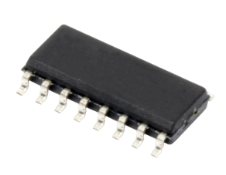
Analog Devices Inc.The AD7887 is a high speed, low power, 12-bit analog-to-digital converter (ADC) that operates from a single 2.7 V to 5.25 V power supply. The AD7887 is capable of 125 kSPS throughput rate. The input track-and-hold acquires a signal in 500 ns and features a single-ended sampling scheme. The output coding for the AD7887 is straight binary, and the part is capable of converting full power signals of up to 2.5 MHz.The AD7887 can be configured for either dual- or single-channel operation via the on-chip control register. There is a default single-channel mode that allows the AD7887 to be operated as a read-only ADC. In single-channel operation, there is one analog input (AIN0) and the AIN1/VREF pin assumes its VREF function. This VREF pin allows the user access to the part’s internal 2.5 V reference, or the VREF pin can be overdriven by an external reference to provide the reference voltage for the part. This external reference voltage has a range of 2.5 V to VDD. The analog input range on AIN0 is 0 to VREF.In dual-channel operation, the AIN1/VREF pin assumes its AIN1 function, providing a second analog input channel. In this case, the reference voltage for the part is provided via the VDD pin. As a result, the input voltage range on both the AIN0 and AIN1 inputs is 0 to VDD.CMOS construction ensures low power dissipation of typically 2 mW for normal operation and 3 μW in power-down mode. The part is available in an 8-lead, 0.15-inch-wide narrow body SOIC and an 8-lead MSOP package.Product HighlightsSmallest 12-bit dual-/single-channel ADC; 8-lead MSOP package.Lowest power 12-bit dual-/single-channel ADC.Flexible power management options, including automatic power-down after conversion.Read-only ADC capability.Analog input range from 0 V to VREF.Versatile serial input/output port (SPI/QSPI/MICROWIRE/ DSP compatible).ApplicationsBattery-powered systems (personal digital assistants, medical instruments, mobile communications)Instrumentation and control systemsHigh speed modems
AD7890ANZ-10
Part Number : AD7890ANZ-10
Analog Devices Inc.The AD7890 is an 8-channel 12-bit data acquisition system. The part contains an input multiplexer, an on-chip track/hold amplifier, a high speed 12-bit ADC, a 2.5 V reference, and a high speed, serialinterface. The part operates from a single 5 V supply and accepts an analog input range of ±10 V (AD7890-10), 0 V to 4.096 V (AD7890-4), and 0 V to 2.5 V (AD7890-2).The multiplexer on the part is independently accessible. This allows the user to insert an antialiasing filter or signal conditioning, if required, between the multiplexer and the ADC. This means that one antialiasing filter can be used for all eight channels. Connection of an external capacitor allows the user to adjust the time given to the multiplexer settling to include any external delays in the filter or signal conditioning circuitry.Output data from the AD7890 is provided via a high speed bidirectional serial interface port. The part contains an on-chip control register, allowing control of channel selection, conversion start, and power-down via the serial port. Versatile, high speed logic ensures easy interfacing to serial ports on microcontrollers and digital signal processors.In addition to the traditional dc accuracy specifications such as linearity, full-scale, and offset errors, the AD7890 is also specified for dynamic performance parameters including harmonic distortion and signal-to-noise ratio.Power dissipation in normal mode is low at 30 mW typical and the part can be placed in a standby (power-down) mode if it is not required to perform conversions. The AD7890 is fabricated in Analog Devices, Inc.'s Linear Compatible CMOS (LC2MOS) process, a mixed technology process that combines precision bipolar circuits with low power CMOS logic. The part is available in a 24-lead, 0.3' wide, plastic or ceramic dual-in-line package or in a 24-lead small outline package (SOIC_W).PRODUCT HIGHLIGHTS Complete 12-Bit Data Acquisition System-on-a-Chip. The AD7890 is a complete monolithic ADC combining an 8-channel multiplexer, 12-bit ADC, 2.5 V reference, and a track/hold amplifier on a single chip. Separate Access to Multiplexer and ADC. The AD7890 provides access to the output of the multiplexer allowing one antialiasing filter for 8 channels—a considerable savings over the 8 antialiasing filters required if the multiplexer is internally connected to the ADC. High Speed Serial Interface. The part provides a high speed serial interface for easy connection to serial ports of microcontrollers and DSP processors.
AD8052ARZ
Part Number : AD8052ARZ
Analog Devices Inc.The AD8051 (single), AD8052 (dual) and AD8054 (quad) arelow cost, high speed, voltage feedback amplifiers. The amplifiers operate on +3 V, +5 V or ±5 V supplies at low supply current. They have true single-supply capability with an input voltage range extending 200 mV below the negative rail and within 1 V of the positive rail.Despite their low cost, the AD8051/AD8052/AD8054 provideexcellent overall performance and versatility. The output voltageswings to within 25 mV of each rail, providing themaximum output dynamic range with excellent overdrive recovery.The AD8051/AD8052/AD8054 are well suited for video electronics, cameras, video switchers, or any high speed portable equipment. Low distortion and fast settling make them ideal for active filter applications.The AD8051/AD8052 in the 8-lead SOIC, the AD8052 in the MSOP, the AD8054 in the 14-lead SOIC, and the 14-lead TSSOP packages are available in the extended temperature range of −40°C to +125°C.ApplicationsActive filtersAnalog-to-digital driversClock bufferConsumer videoProfessional camerasCCD imaging systemsCD/DVD ROMs
AD822BRZ-REEL
Part Number : AD822BRZ-REEL
Analog Devices Inc.The AD822 is a dual precision, low power FET input op ampthat can operate from a single supply of 5 V to 30 V or dual supplies of ±2.5 V to ±15 V. It has true single-supply capability with an input voltage range extending below the negative rail, allowing the AD822 to accommodate input signals belowground in the single-supply mode. Output voltage swing extends to within 10 mV of each rail, providing the maximumoutput dynamic range.Offset voltage of 800 μV maximum, offset voltage drift of 2 μV/°C, input bias currents below 25 pA, and low input voltage noise provide dc precision with source impedances up to a gigaohm. The 1.8 MHz unity-gain bandwidth, –93 dB THD at 10 kHz,and 3 V/μs slew rate are provided with a low supply current of 800 μA per amplifier.Applications Battery-powered precision instrumentation Photodiode preamps Active filters 12-bit to 14-bit data acquisition systems Medical instrumentation Low power references and regulatorsThe AD822-EP supports defense and aerospace applications (AQEC standard)
AD8400ARZ1
Part Number : AD8400ARZ1
Analog Devices Inc.The AD8400 / AD8402 / AD8403 provide a single, dual or quad channel, 256 position digitally controlled variable resistor (VR) device. These devices perform the same electronic adjustment function as a potentiometer or variable resistor. The AD8400 contains a single variable resistor in the compact SO-8 package. The AD8402 contains two independent variable resistors in saving SO-14 surface mount package. The AD8403 contains four independent variable resistors in 24-lead PDIP, SOIC and TSSOP packages. Each part contains a fixed resistor with a wiper contact that taps the fixed resistor value at a point determined by a digital code loaded into the controlling serial input register. The resistance between the wiper and either endpoint of the fixed resistor varies linearly with respect to the digital code transferred into the VR latch. Each variable resistor offers a completely programmable value of resistance, between the A terminal and the wiper or the B terminal and the wiper. The fixed A to B terminal resistance of 1 kOhm, 10 kOhm, 50 kOhm or 100 kOhm has a ±1% channel-to-channel matching tolerance with a nominal temperature coefficient of 500 ppm/°C. A unique switching circuit minimizes the high glitch inherent in traditional switched resistor designs avoiding any make-before-break or break-before-make operation.Each VR has its own VR latch that holds its programmed resistance value. These VR latches are updated from an SPI compatible serial-to-parallel shift register that is loaded from a standard 3-wire serial-input digital interface. Ten data bits make up the data word clocked into the serial input register. The data word is decoded where the first two bits determine the address of the VR latch to be loaded, the last eight bits are data. A serial data output pin at the opposite end of the serial register allows simple daisy-chaining in multiple VR applications without additional external decoding logic.APPLICATIONS Mechanical potentiometer replacement Programmable filters, delays, time constants Volume control, panning Line impedance matching Power supply adjustment
AD8402ARZ1
Part Number : AD8402ARZ1
Analog Devices Inc.The AD8400/AD8402/AD8403 provide a single, dual or quad channel, 256 position digitally controlled variable resistor (VR) device. These devices perform the same electronic adjustment function as a potentiometer or variable resistor. The AD8400 contains a single variable resistor in the compact SO-8 package. The AD8402 contains two independent variable resistors in saving SO-14 surface mount package. The AD8403 contains four independent variable resistors in 24-lead PDIP, SOIC and TSSOP packages. Each part contains a fixed resistor with a wiper contact that taps the fixed resistor value at a point determined by a digital code loaded into the controlling serial input register. The resistance between the wiper and either endpoint of the fixed resistor varies linearly with respect to the digital code transferred into the VR latch. Each variable resistor offers a completely programmable value of resistance, between the A terminal and the wiper or the B terminal and the wiper. The fixed A to B terminal resistance of 1 kOhm, 10 kOhm, 50 kOhm or 100 kOhm has a ±1% channel-to-channel matching tolerance with a nominal temperature coefficient of 500 ppm/°C. A unique switching circuit minimizes the high glitch inherent in traditional switched resistor designs avoiding any make-before-break or break-before-make operation.Each VR has its own VR latch that holds its programmed resistance value. These VR latches are updated from an SPI compatible serial-to-parallel shift register that is loaded from a standard 3-wire serial-input digital interface. Ten data bits make up the data word clocked into the serial input register. The data word is decoded where the first two bits determine the address of the VR latch to be loaded, the last eight bits are data. A serial data output pin at the opposite end of the serial register allows simple daisy-chaining in multiple VR applications without additional external decoding logic.
AD8402ARZ50
Part Number : AD8402ARZ50
Analog Devices Inc.The AD8400/AD8402/AD8403 provide a single, dual or quad channel, 256 position digitally controlled variable resistor (VR) device. These devices perform the same electronic adjustment function as a potentiometer or variable resistor. The AD8400 contains a single variable resistor in the compact SO-8 package. The AD8402 contains two independent variable resistors in saving SO-14 surface mount package. The AD8403 contains four independent variable resistors in 24-lead PDIP, SOIC and TSSOP packages. Each part contains a fixed resistor with a wiper contact that taps the fixed resistor value at a point determined by a digital code loaded into the controlling serial input register. The resistance between the wiper and either endpoint of the fixed resistor varies linearly with respect to the digital code transferred into the VR latch. Each variable resistor offers a completely programmable value of resistance, between the A terminal and the wiper or the B terminal and the wiper. The fixed A to B terminal resistance of 1 kOhm, 10 kOhm, 50 kOhm or 100 kOhm has a ±1% channel-to-channel matching tolerance with a nominal temperature coefficient of 500 ppm/°C. A unique switching circuit minimizes the high glitch inherent in traditional switched resistor designs avoiding any make-before-break or break-before-make operation.Each VR has its own VR latch that holds its programmed resistance value. These VR latches are updated from an SPI compatible serial-to-parallel shift register that is loaded from a standard 3-wire serial-input digital interface. Ten data bits make up the data word clocked into the serial input register. The data word is decoded where the first two bits determine the address of the VR latch to be loaded, the last eight bits are data. A serial data output pin at the opposite end of the serial register allows simple daisy-chaining in multiple VR applications without additional external decoding logic.
AD9540BCPZ
Part Number : AD9540BCPZ
Analog Devices Inc.The AD9540 is Analog Devices’ first dedicated clockingproduct specifically designed to support the extremely stringentclocking requirements of the highest performance dataconverters. The device features high performance PLL (phase-lockedloop) circuitry, including a flexible 200 MHz phasefrequency detector and a digitally controlled charge pumpcurrent. The device also provides a low jitter, 655 MHz CML-mode,PECL-compliant output driver with programmable slewrates. External VCO rates up to 2.7 GHz are supported.Extremely fine tuning resolution (steps less than 2.33 µHz) isanother feature supported by this device. Information is loadedinto the AD9540 via a serial I/O port that has a device writespeed of 25 Mbps. The AD9540 frequency divider block canalso be programmed to support a spread spectrum mode ofoperation.The AD9540 is specified to operate over the extendedautomotive range of −40°C to +85°C.Applications Clocking high performance data converters Base station clocking applications Network (SONET/SDH) clocking Gigabit Ethernet (GbE) clocking Instrumentation clocking circuits Agile LO frequency synthesis Automotive radar FM chirp source for radar and scanning systems Test and measurement equipment Acousto-optic device drivers
AD9835BRUZ
Part Number : AD9835BRUZ
Analog Devices Inc.The AD9835 is a numerically-controlled oscillator employing a phase accumulator, a COS lookup table, and a 10-bit digital-to-analog converter integrated on a single CMOS chip. Modulation capabilities are provided for phase modulation and frequency modulation.Clock rates of up to 50 MHz are supported. Frequency accuracycan be controlled to one part in 4 billion. Modulation is effected by loading registers through the serial interface. A power-down bit allows the user to power down the AD9835 when it is not in use, the power consumption reduces to 1.75 mW.The part is available in a 16-lead TSSOP package.APPLICATIONS Frequency stimulus/waveform generation Frequency phase tuning and modulation Low power RF/communications systems Liquid and gas flow measurement Sensory applications: proximity, motion, and defect detection Test and medical equipment
AD9923ABBCZ
Part Number : AD9923ABBCZ
Analog Devices Inc.The AD9923A is a complete 36 MHz front-end solution for digital still cameras and other CCD imaging applications. Similar to the AD9923 product, the AD9923A includes the analog front end (AFE), a fully programmable timing generator (TG), and a 15-channel vertical driver (V-driver). A Precision Timing core allows adjustment of high speed clocks with approximately 600 ps resolution at 36 MHz operation.The on-chip V-driver supports up to 15 channels for use with 5-field, 10-phase CCDs.The analog front end includes black level clamping, CDS, VGA, and a 12-bit ADC. The timing generator and V-driver provide all the necessary CCD clocks: RG, H-clocks, vertical clocks, sensor gate pulses, substrate clock, and substrate bias control. The internal registers are programmed using a 3-wire serial interface.Packaged in an 8 mm × 8 mm CSP_BGA, the AD9923A is specified over an operating temperature range of −25°C to +85°C.APPLICATIONS Digital still cameras
AD9952YSVZ
Part Number : AD9952YSVZ
Analog Devices Inc.The AD9952 is a direct digital synthesizer (DDS) featuring a 14-bit DAC (digital-to-analog converter) and operating up to 400 MSPS. The AD9952 uses advanced DDS technology, coupled with an internal high speed, high performance DAC to form a digitally programmable, complete high frequency synthesizer capable of generating a frequency-agile analog output sinusoidal waveform at up to 200 MHz. The AD9952 isdesigned to provide fast frequency hopping and fine tuningresolution (32-bit frequency tuning word). The frequency tuning and control words are loaded into the AD9952 via a serial I/O port. The AD9952 is specified to operate over the extended industrial temperature range of −40°C to +105°C.Applications Agile LO frequency synthesis Programmable clock generators Test and measurement equipment Acousto-optic device drivers
ADA4841-2YRZ-RL
Part Number : ADA4841-2YRZ-RL
Analog Devices Inc.The ADA4841-2 is a unity gain stable, low noiseand distortion, rail-to-rail output amplifier that has a quiescentcurrent of 1.5 mA maximum. In spite of its low powerconsumption, this amplifier offers low wideband voltagenoise performance of 2.1 nV/√Hz and 1.4 pA/√Hz current noise,along with excellent spurious-free dynamic range (SFDR) of−105 dBc at 100 kHz. To maintain a low noise environment atlower frequencies, the amplifier has low 1/f noise of 7 nV/√Hzand 13 pA/√Hz at 10 Hz.The ADA4841-2 output can swing to less than50 mV of either rail. The input common-mode voltage rangeextends down to the negative supply. The ADA4841-2 can drive up to 10 pF of capacitive load withminimal peaking.The ADA4841-2 provides the performance requiredto efficiently support emerging 16-bit to 18-bit ADCs and is ideal for portable instrumentation, high channel count, industrialmeasurement, and medical applications. The ADA4841-1 is ideally suited to drive the AD7685/AD7686,16-bit PulSAR ADCs.The ADA4841-2 package features RoHS compliantlead finishes. The amplifier is rated to work over theindustrial temperature range (−40°C to +125°C).Applications Low power, low noise signal processing Battery-powered instrumentation 16-bit PulSAR® ADC drivers
ADF4002BCPZ
Part Number : ADF4002BCPZ
Analog Devices Inc.The ADF4002 frequency synthesizer is used to implement local oscillators in the up-conversion and down-conversion sections of wireless receivers and transmitters. It consists of a low-noise digital phase frequency detector (PFD), a precision charge pump, a programmable reference divider and programmable N divider. The 14-bit reference counter (R counter), allows selectable REFIN frequencies at the PFD input.A complete phase-locked loop (PLL) can be implemented if the synthesizer is used with an external loop filter and voltage controlled oscillator (VCO). In addition, by programming R and N to 1, the device can be used as a standalone PFD and charge pump.The ADF4002-EP supports defense and aerospace applications (AQEC standard).
ADF4111BRUZ
Part Number : ADF4111BRUZ
Analog Devices Inc.The ADF4110 family of frequency synthesizers can be used to implement local oscillators in the up-conversion and down-conversion sections of wireless receivers and transmitters. They consist of low-noise digital PFD (Phase Frequency Detector), a precision charge pump, a programmable reference divider, programmable A and B counters and a dual modulus prescaler (P/P+1). The A (6-bit) and B (13-bit) counters, in conjunction with the dual modulus prescaler (P/P+1), implement an N divider (N = BP+A). In addition, the 14-bit reference counter (R Counter), allows selectable REFIN frequencies at the PFD input. A complete PLL (Phase-Locked Loop) can be implemented if the synthesizer is used with an external loop filter and VCO (Voltage Controlled Oscillator).Control of all the on-chip registers is via a simple 3-wire interface. The devices operate with a power supply ranging from 2.7 V to 5.5 V and can be powered down when not in use.
ADG1212YRUZ
Part Number : ADG1212YRUZ
Analog Devices Inc.The ADG1211 / ADG1212 / ADG1213 are monolithic complementary metal-oxide semiconductor (CMOS) devices containing four independently selectable switches designed on an iCMOS® (industrial CMOS) process. iCMOS is a modular manufacturing process combining high voltage CMOS and bipolar technologies. It enables the development of a wide range of high performance analog ICs capable of 33 V operation in a footprint that no previous generation of high voltage devices has been able to achieve. Unlike analog ICs using conventional CMOS processes, iCMOS components can tolerate high supply voltages while providing increased performance, dramatically lower power consumption, and reduced package size.The ultralow capacitance and charge injection of these switches make them ideal solutions for data acquisition and sample-and-hold applications, where low glitch and fast settling are required. Fast switching speed coupled with high signal bandwidth make the devices suitable for video signal switching.iCMOS construction ensures ultralow power dissipation, making the devices ideally suited for portable and battery-powered instruments.The ADG1211 / ADG1212 / ADG1213 contain four independent single-pole/single-throw (SPST) switches. The ADG1211 and ADG1212 differ only in that the digital control logic is inverted. The ADG1211 switches are turned on with Logic 0 on the appropriate control input, while Logic 1 is required for the ADG1212. The ADG1213 has two switches with digital control logic similar to that of the ADG1211; the logic is inverted on the other two switches. The ADG1213 exhibits break-before-make switching action for use in multiplexer applications.Each switch conducts equally well in both directions when on and has an input signal range that extends to the supplies. In the off condition, signal levels up to the supplies are blocked.PRODUCT HIGHLIGHTS Ultralow capacitance.
ADG202AKNZ
Part Number : ADG202AKNZ
Analog Devices Inc.The ADG202A is a monolithic CMOS device comprising four independently selectable switches. They are designed on an enhanced LC2MOS process, which gives an increased signal handling capability of ±15 V. These switches also feature high switching speeds and low RON. The ADG202A switches are turned on with a logic high on the appropriate control input. Each switch conducts equally well in both directions when ON and each has an input signal range that extends to the supplies. All switches exhibit break-before-make switching action for use in multiplexer applications. Inherent in the design is low charge injection for minimum transients when switching the digital inputs.
ADG3245BCPZ
Part Number : ADG3245BCPZ
Analog Devices Inc.The ADG3245 is a 2.5 V or 3.3 V, 8-bit, 2-port digital switch.It is designed on Analog Devices’ low voltage CMOS process,which provides low power dissipation yet gives high switchingspeed and very low on resistance, allowing inputs to be connectedto outputs without additional propagation delay or generatingadditional ground bounce noise.The switches are enabled by means of the bus enable (BE) inputsignal. These digital switches allow bidirectional signals to beswitched when ON. In the OFF condition, signal levels up tothe supplies are blocked.This device is ideal for applications requiring level translation.When operated from a 3.3 V supply, level translation from 3.3 Vinputs to 2.5 V outputs is allowed. Similarly, if the device isoperated from a 2.5 V supply and 2.5 V inputs are applied, thedevice will translate the outputs to 1.8 V. In addition to this, alevel translating select pin (SEL) is included. When SEL is low,VCC is reduced internally, allowing for level translation between3.3 V inputs and 1.8 V outputs. This makes the device suited toapplications requiring level translation between different supplies,such as converter to DSP/microcontroller interfacing.APPLICATIONS 3.3 V to 1.8 V voltage translation 3.3 V to 2.5 V voltage translation 2.5 V to 1.8 V voltage translation Bus switching Bus isolation Hot swap Hot plug Analog switch applicationsPRODUCT HIGHLIGHTS 3.3 V or 2.5 V supply operation Extremely low propagation delay through switch 4.5 Ω switches connect inputs to outputs Level/voltage translation 20-lead TSSOP and LFCSP (4 mm × 4 mm) packages
ADG408BRUZ
Part Number : ADG408BRUZ
Analog Devices Inc.The ADG408 is a monolithic CMOS analog multiplexer comprising 8 single channels. The ADG408 switches one of eight inputs to a common output as determined by the 3-bit binary address lines A0, A1 and A2. An EN input is used to enable or disable the device. When disabled, all channels are switched OFF. The ADG408 is designed on an enhanced LC2MOS process which provides low power dissipation yet gives high switching speed and low on resistance. Each channel conducts equally well in both directions when ON and has an input signal range which extends to the supplies. In the OFF condition, signal levels up to the supplies are blocked. All channels exhibit break before make switching action preventing momentary shorting when switching channels. Inherent in the design is low charge injection for minimum transients when switching the digital inputs.
ADG419BNZ
Part Number : ADG419BNZ
Analog Devices Inc.The ADG419 is a monolithic CMOS SPDT switch. This switch is designed on an enhanced LC2MOS process that provides low power dissipation yet gives high switching speed, low on resistance, and low leakage currents.The on resistance profile of the ADG419 is very flat over the full analog input range, ensuring excellent linearity and low distortion. The part also exhibits high switching speed and high signal bandwidth. CMOS construction ensures ultralow power dissipation, making the parts ideally suited for portable and battery-powered instruments.Each switch of the ADG419 conducts equally well in both directions when on and has an input signal range that extends to the supplies. In the off condition, signal levels up to the supplies are blocked. The ADG419 exhibits break-before-make switching action.The ADG419-EP supports defense and aerospace applications (AQEC)Applications Precision test equipment Precision instrumentation Battery-powered systems Sample-and-hold systems
ADG508FBRWZ
Part Number : ADG508FBRWZ
Analog Devices Inc.The ADG508F and ADG509F are CMOS analog multiplexers, with the ADG508F comprising eight single channels and the ADG509F comprising four differential channels. These multiplexer provides fault protection. Using a series n-channel, p-channel, n-channel MOSFET structure, both device and signal source protection is provided in the event of an overvoltage or power loss. The multiplexer can withstand continuous overvoltage inputs from -40 V to +55 V. During fault conditions with power supplies off, the multiplexer input (or output) appears as an open circuit and only a few nanoamperes of leakage current will flow. This protects not only the multiplexer and the circuitry driven by the multiplexer, but also protects the sensors or signal sources that drive the multiplexer.The ADG508F switches one of eight inputs to a common output as determined by the 3-bit binary address lines A0, A1 and A2. The ADG509F switches one of four differential inputs to a common differential output as determined by the 2-bit binary address lines A0 and A1. An EN input on each device is used to enable or disable the device. When disabled, all channels are switched OFF.PRODUCT HIGHLIGHTS Fault protection. The ADG508F/ADG509F can withstand continuous voltage inputs from −40 V to +55 V. When a fault occurs due to the power supplies being turned off, all the channels are turned off and only a leakage current of a few nanoamperes flows. On channel saturates while fault exists. Low RON. Fast switching times. Break-before-make switching. Switches are guaranteed break-before-make so that input signals are protected against momentary shorting. Trench isolation eliminates latch-up. A dielectric trench separates the p and n-channel MOSFETs thereby preventing latch-up.APPLICATIONS Existing multiplexer applications (both fault-protected and nonfault-protected) New designs requiring multiplexer functions


