AD8641AKSZ-REEL7
Part Number : AD8641AKSZ-REEL7
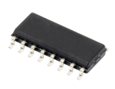
Analog Devices Inc.The AD8641/AD8642/AD8643 are low power, precision JFET input amplifiers featuring extremely low input bias current and rail-to-rail output. The ability to swing nearly rail-to-rail at the input and rail-to-rail at the output enables designers to buffer CMOS DACs, ASICs, and other wide output swing devices in single-supply systems. The outputs remain stable with capacitive loads of more than 500 pF.The AD8641/AD8642/AD8643 are suitable for applications utilizing multichannel boards that require low power to manage heat. Other applications include photodiodes, ATE reference level drivers, battery management, and industrial controls.The AD8641/AD8642/AD8643 are fully specified over the extended industrial temperature range of –40°C to +125°C. The AD8641 is available in 5-lead SC70 and 8-lead SOIC lead-free packages. The AD8642 is available in 8-lead MSOP and 8-lead SOIC lead-free packages. The AD8643 is available in 14-lead SOIC and 16-lead, 3 mm × 3 mm, LFCSP lead-free packages.ApplicationsLine-/battery-powered instrumentsPhotodiode amplifiersPrecision current sensingMedical instrumentationIndustrial controlsPrecision filtersPortable audioATE
AD8671ARMZ
Part Number : AD8671ARMZ
Analog Devices Inc.The AD8671/AD8672/AD8674 are very high precision amplifiers featuring very low noise, very low offset voltage and drift, low input bias current, 10 MHz bandwidth, and low power consumption. Outputs are stable with capacitive loads of over 1000 pF. Supply current is less than 3 mA per amplifier at 30 V.The AD8671/AD8672/AD8674’s combination of ultralow noise, high precision, speed, and stability is unmatched. The MSOP version of the AD8671/AD8672 requires only half the board space of comparable amplifiers.Applications for these amplifiers include high quality PLL filters, precision filters, medical and analytical instrumentation, precision power supply controls, ATE, data acquisition, and precision controls as well as professional quality audio.The AD8671/AD8672 are specified over the extended industrial temperature range (−40°C to +125°C), and the AD8674 is specified over the industrial temperature range (−40°C to +85°C).The AD8671/AD8672 are available in the 8-lead SOIC and 8-lead MSOP packages. The AD8674 is available in 14-lead SOIC and 14-lead TSSOP packages.Surface-mount devices in MSOP packages are available in tape and reel only.APPLICATIONSPLL filtersFilters for GPSInstrumentationSensors and controlsProfessional quality audio
AD976ACRZ
Part Number : AD976ACRZ
Analog Devices Inc.The AD976 and AD976A are high-speed, low-power 16-bit A/D converters with each operating from a single 5 V supply. The AD976A has a throughput rate of 200 ksps whereas the AD976 has a throughput rate of 100 ksps. Each part contains a successive approximation, switched capacitor ADC, an internal 2.5 V reference, and a high-speed parallel interface. The AD976 and AD976A dissipate a maximum of 100 mW. The ADC is factory calibrated to minimize all linearity errors. The analog full-scale input is the standard industrial range of ±10 V.The AD976 and AD976A are comprehensively tested for ac parameters such as SNR and THD, as well as the more traditional parameters of offset, gain and linearity. The AD976 and AD976A are fabricated on Analog Devices' proprietary BiCMOS process, which has high performance bipolar devices along with CMOS transistors. The AD976 and AD976A are available in skinny 28-pin DIP, SSOP and SOIC packages.
ADCMP370AKSZ-REEL7
Part Number : ADCMP370AKSZ-REEL7
Analog Devices Inc.The ADCMP370 / ADCMP371 are general purpose comparators with input offset voltages of 6mV (max). High performance over the -40°C to +85°C temperature range make them suitable for use in automotive and other thermally harsh applications, while low power consumption and space efficientSC70 packaging make them ideal for battery powered portable equipment.The ADCMP371 has a push-pull output stage, while theADCMP370 has an open-drain output. The inputs on bothparts and the output on the ADCMP370 can tolerate voltagesup to 22 V, making them suitable for use as voltage detectors inportable equipment. The devices are available in space-efficient, 5-lead SC70packaging.APPLICATIONS Voltage Detectors Battery Management Systems A/D Converters Low Voltage Applications Battery Powered Electronics Portable Equipment
ADE7752AARZ
Part Number : ADE7752AARZ
Analog Devices Inc.The ADE7752A is an accurate active energy measurement IC intended for use in any 3-phase distribution system. It provides instantaneous and average real power based on line current and voltage. The part specifications surpass the accuracy requirements as quoted in the IEC61036 standard. The only analog circuitry used in the ADE7752A is in the ADCs and reference circuit. All other signal processing (e.g., multiplication and filtering) is carried out in the digital domain. This approach provides superior stability and accuracy over extremes in environmental conditions and over time.Gain calibration between channels is adjusted external to this device. The ADE7752A is available in 24-lead SOIC package. The power consumption of ADE7752A is lower than ADE7752. ADE7752A is recommended for all new designs and may be used as a direct replacement for ADE7752. The parts are functionality and pin compatible.For additional technical information on your ADE7752A meter design, see AN-641: A 3-Phase Power Meter Based on the ADE7752 (pdf, 507,533 bytes).
ADF4360-8BCPZ
Part Number : ADF4360-8BCPZ
Analog Devices Inc.The ADF4360-8 is an integrated integer-N synthesizer and voltagecontrolled oscillator (VCO). The ADF4360-8 center frequencyis set by external inductors. This allows a frequencyrange of between 65 MHz to 400 MHz. Control of all the on-chip registers is through a simple 3-wire interface. The device operates with a power supply ranging from 3.0 V to 3.6 V and can be powered down when not in use.
ADG406BNZ
Part Number : ADG406BNZ
Analog Devices Inc.The ADG406, ADG407, and ADG426 are monolithic CMOS analog multiplexers. The ADG406 and ADG426 switch one of sixteen inputs to a common output as determined by the 4-bit binary address lines: A0, A1, A2, and A3. The ADG426 has on-chip address and control latches that facilitate microprocessor interfacing. The ADG407 switches one of eight differential inputs to a common differential output as determined by the 3-bit binary address lines A0, A1 and A2. An EN input on all devices is used to enable or disable the device. When disabled, all channels are switched off.The ADG406 / ADG407 / ADG426 are designed on an enhanced LC2MOS process that provides low power dissipation yet gives high switching speed and low on resistance. These features make the parts suitable for high speed data acquisition systems and audio signal switching. Low power dissipation makes the parts suitable for battery powered systems. Each channel conducts equally well in both directions when on and has an input signal range which extends to the supplies. In the off condition, signal levels up to the supplies are blocked. All channels exhibit break-before-make switching action preventing momentary shorting when switching channels. Inherent in the design is low charge injection for minimum transients when switching the digital inputs.
ADG411BNZ
Part Number : ADG411BNZ
Analog Devices Inc.The ADG411 is a monolithic CMOS device comprising four independently selectable switches. It is designed on an enhanced LC2MOS process which provides low power dissipation yet gives high switching speed and low on resistance.The ADG411 switches are turned on with a logic low on the appropriate control input. Each switch conducts equally well in both directions when ON and each has an input signal range that extends to the supplies. All switches exhibit break-before-make switching action for use in multiplexer applications. Inherent in the design is low charge injection for minimum transients when switching the digital inputs.
ADG452BRUZ
Part Number : ADG452BRUZ
Analog Devices Inc.The ADG452 is a monolithic CMOS device comprising four independently selectable switches. It is designed on an enhanced LC2MOS process which provides low power dissipation yet gives high switching speed and low on resistance.The ADG452 switches are turned on with a logic high on the appropriate control input. Each switch conducts equally well in both directions when ON and each has an input signal range that extends to the supplies. All switches exhibit break-before-make switching action for use in multiplexer applications. Inherent in the design is low charge injection for minimum transients when switching the digital inputs.
ADM1485ARZ
Part Number : ADM1485ARZ
Analog Devices Inc.The ADM1485 is a differential line transceiver suitable for high speed bidirectional data communication on multipoint bus transmission lines. It is designed for balanced data transmission and complies with both EIA Standards RS-485 and RS-422. The part contains a differential line driver and a differential line receiver. Both the driver and the receiver may be enabled independently. When disabled, the outputs are tristated.The ADM1485 operates from a single +5 V power supply. Excessive power dissipation caused by bus contention or by output shorting is prevented by a thermal shutdown circuit. This feature forces the driver output into a high impedance state if during fault conditions a significant temperature increase is detected in the internal driver circuitry.Up to 32 transceivers may be connected simultaneously on a bus, but only one driver should be enabled at any time. It is important therefore that the remaining disabled drivers do not load the bus. To ensure this, the ADM1485 driver features high output impedance when disabled and also when powered down.This minimizes the loading effect when the transceiver is not being utilized. The high impedance driver output is maintained over the entire common-mode voltage range from -7 V to +12 V.The receiver contains a fail safe feature which results in a logic high output state if the inputs are unconnected (floating).The ADM1485 is fabricated in BiCMOS, an advanced mixed technology process combining low power CMOS with fast switching bipolar technology. All inputs and outputs contain protection against ESD; all driver outputs feature high source and sink current capability. An epitaxial layer is used to guard against latch-up.The ADM1485 features extremely fast switching speeds. Minimal driver propagation delays permit transmission at data rates up to 30 Mbits/s while low skew minimizes EMI interference.The part is fully specified over the commercial and industrial temperature range and is available in an 8-pin DIL/SOIC package.
ADM206ANZ
Part Number : ADM206ANZ
Analog Devices Inc.The ADM2xx family of line drivers/receivers is intended for all EIA-232-E and V.28 communications interfaces, especially in applications where ±12 V is not available. The ADM205, ADM211 and ADM213 feature a low power shutdown mode which reduces power dissipation to less than 5 µW making them ideally suited for battery powered equipment. The ADM205 does not require any external components and is particularly useful in applications where printed circuit board space critical. The ADM213 has an active-low shutdown and an active-high receiver enable control. Two receivers of the ADM213 remain active during shutdown. This feature is useful for ring indicator monitoring.All members of the ADM2xx family, except the ADM209, include two internal charge pump voltage converters which allow operation from a single +5 V supply. These converters convert the +5 V input power to the ±10 V required for RS-232 output levels. The ADM209 is designed to operate from +5 V and +12 V supplies. An internal +12 V to −12 V charge pump voltage converter generates the −12 V supply.
ADM207ARZ
Part Number : ADM207ARZ
Analog Devices Inc.The ADM2xx family of line drivers/receivers is intended for all EIA-232-E and V.28 communications interfaces, especially in applications where ±12 V is not available. The ADM205, ADM211 and ADM213 feature a low power shutdown mode which reduces power dissipation to less than 5 µW making them ideally suited for battery powered equipment. The ADM205 does not require any external components and is particularly useful in applications where printed circuit board space critical. The ADM213 has an active-low shutdown and an active-high receiver enable control. Two receivers of the ADM213 remain active during shutdown. This feature is useful for ring indicator monitoring.All members of the ADM2xx family, except the ADM209, include two internal charge pump voltage converters which allow operation from a single +5 V supply. These converters convert the +5 V input power to the ±10 V required for RS-232 output levels. The ADM209 is designed to operate from +5 V and +12 V supplies. An internal +12 V to −12 V charge pump voltage converter generates the −12 V supply.
ADM483ARZ
Part Number : ADM483ARZ
Analog Devices Inc.The ADM483 is a low power differential line transceiver suitable for half-duplex data communication on multipoint bus trans-mission lines. It is designed for balanced data transmission, and complies with EIA Standards RS-485 and RS-422.The part contains a differential line driver and a differential line receiver. Both share the same differential pins, with either the driver or the receiver being enabled at any given time.The device has an input impedance of 12 kΩ, allowing up to 32 transceivers on one bus. Since only one driver should be enabled at any time, the output of a disabled or powered-down driver is three-stated to avoid overloading the bus. This high impedance driver output is maintained over the entire common-mode voltage range from –7 V to +12 V.The receiver contains a fail-safe feature that results in a logic high output state if the inputs are unconnected (floating). The driver outputs are slew-rate limited to reduce EMI and data errors caused by reflections from improperly terminated buses. Excessive power dissipation caused by bus contention or by output shorting is prevented by a thermal shutdown circuit. The part is fully specified over the industrial temperature range, and is available in an 8-lead SOIC package.
AD5341BRUZ
Part Number : AD5341BRUZ
Analog Devices Inc.The AD5330/AD5331/AD5340/AD5341* are single 8-/10-/12-bit DACs. They operate from a 2.5 V to 5.5 V supply consuming just 115 μA at 3 V and feature a power-down mode that further reduces the current to 80 nA. The devices incorporate an on-chip output buffer that can drive the output to both supply rails, but the AD5330, AD5340, and AD5341 allow a choice of buffered or unbuffered reference input. The AD5330/AD5331/AD5340/AD5341 have a parallel interface. CS selects the device and data is loaded into the input registers on the rising edge of WR. The GAIN pin allows the output range to be set at 0 V to VREF or 0 V to 2 × VREF. Input data to the DACs is double-buffered, allowing simultaneous update of multiple DACs in a system using the LDAC pin. An asynchronous CLR input is also provided, which resets the contents of the input register and the DAC register to all zeros. These devices also incorporate a power-on reset circuit that ensures that the DAC output powers on to 0 V and remains there until valid data is written to the device. The AD5330/AD5331/AD5340/AD5341 are available in thin shrink small outline packages (TSSOP).ApplicationsPortable battery-powered instruments Digital gain and offset adjustment Programmable voltage and current sources Programmable attenuators Industrial process control * Protected by U.S. Patent Number 5,969,657; other patents pending. Data Sheet, Rev. A, 2/08
AD5445YRUZ-REEL
Part Number : AD5445YRUZ-REEL
Analog Devices Inc.The AD5424 / AD5433 / AD5445 are CMOS 8-, 10-, and 12-bitcurrent output digital-to-analog converters (DACs), respectively.These devices operate from a 2.5 V to 5.5 V power supply,making them suitable for battery-powered applications andmany other applications. These DACs utilize data readback,allowing the user to read the contents of the DAC register viathe DB pins. On power-up, the internal register and latches arefilled with 0s and the DAC outputs are at zero scale.As a result of manufacturing with a CMOS submicron process,they offer excellent 4-quadrant multiplication characteristics,with large signal multiplying bandwidths of up to 10 MHz.The applied external reference input voltage (VREF) determines thefull-scale output current. An integrated feedback resistor (RFB)provides temperature tracking and full-scale voltage outputwhen combined with an external I-to-V precision amplifier.While these devices are upgrades of the AD5424 / AD5433 /AD5445 in multiplying bandwidth performance, they have alatched interface and cannot be used in transparent mode.The AD5424 is available in a small, 20-lead LFCSP and a small,16-lead TSSOP, while the AD5433 and AD5445 DACs are availablein a small, 20-lead LFCSP and a small, 20-lead TSSOP.The EVAL-AD5445SDZ evaluation board is available forevaluating DAC performance. For more information, see theUG-333 evaluation board user guide.APPLICATIONS Portable battery-powered applications Waveform generators Analog processing Instrumentation applications Programmable amplifiers and attenuators Digitally controlled calibration Programmable filters and oscillators Composite video Ultrasound Gain, offset, and voltage trimming
AD5532ABCZ-1
Part Number : AD5532ABCZ-1
Analog Devices Inc.The AD5532 is a 32-channel, 14-bit voltage-output DAC with an additional infinite sample-and-hold mode. The selected DAC register is written to via the 3-wire serial interface; VOUT for this DAC is then updated to reflect the new contents of the DAC register. DAC selection is accomplished via Address Bits A0–A4. The output voltage range is determined by the offset voltage at the OFFS_IN pin and the gain of the output amplifier. It is restricted to a range from VSS + 2 V to VDD – 2 V because of the headroom of the output amplifier.The device is operated with AVCC = 5 V ± 5%; DVCC = 2.7 V to 5.25 V; VSS = −4.75 V to −16.5 V; and VDD = 8 V to 16.5 V. The AD5532 requires a stable 3 V reference on REF_IN as well as an offset voltage on OFFS_IN.PRODUCT HIGHLIGHTS 32-channel, 14-bit DAC in one package, guaranteed monotonic. Available in a 74-lead CSPBGA package with a body size of 12 mm ×12 mm. Droopless/infinite sample-and-hold mode.APPLICATIONS Automatic test equipment Optical networks Level setting Instrumentation Industrial control systems Data acquisition Low cost I/O
AD5532ABCZ-2
Part Number : AD5532ABCZ-2
Analog Devices Inc.The AD5532 is a 32-channel, 14-bit voltage-output DAC with an additional infinite sample-and-hold mode. The selected DAC register is written to via the 3-wire serial interface; VOUT for this DAC is then updated to reflect the new contents of the DAC register. DAC selection is accomplished via Address Bits A0–A4. The output voltage range is determined by the offset voltage at the OFFS_IN pin and the gain of the output amplifier. It is restricted to a range from VSS + 2 V to VDD – 2 V because of the headroom of the output amplifier.The device is operated with AVCC = 5 V ± 5%; DVCC = 2.7 V to 5.25 V; VSS = −4.75 V to −16.5 V; and VDD = 8 V to 16.5 V. The AD5532 requires a stable 3 V reference on REF_IN as well as an offset voltage on OFFS_IN.PRODUCT HIGHLIGHTS 32-channel, 14-bit DAC in one package, guaranteed monotonic. Available in a 74-lead CSPBGA package with a body size of 12 mm ×12 mm. Droopless/infinite sample-and-hold mode.APPLICATIONS Automatic test equipment Optical networks Level setting Instrumentation Industrial control systems Data acquisition Low cost I/O
AD570JD
Part Number : AD570JD
Analog Devices Inc.The AD570 is an 8-bit successive approximation A/D converter consisting of a DAC, voltage reference, clock, comparator, successive approximation register and output buffers-all fabricated on a single chip. No external components are required to perform a full accuracy 8-bit conversion in 25 µs.The AD570 incorporates the most advanced integrated circuit design and processing technology available today. I2 L (integrated injection logic) processing in the fabrication of the SAR function along with laser trimming of the high stability SiCr thin-film resistor ladder network at the wafer stage (LWT) and a temperature compensated, subsurface Zener reference insures full 8-bit accuracy at low cost.Operating on supplies of +5 V and -15 V, the AD570 accepts analog inputs of 0 V to +10 V unipolar of ±5 V bipolar, externally selectable. As the BLANK and CONVERT input is driven low, the three-state outputs go into the high impedance state and a conversion commences. Upon completion of the conversion, the DATA READY line goes low and the data appears at the output. Pulling the BLANK and CONVERT input high three states the outputs and readies the device for the next conversion. The AD570 executes a true 8-bit conversion with no missing codes in approximately 25 µs.The AD570 is available in two versions; the AD570J is specified for the 0°C to +70°C temperature range, the AD570S for -55°C to +125°C. Both guarantee full 8-bit accuracy and no missing codes over their respective temperature ranges. PRODUCT HIGHLIGHTS The AD570 is a complete 8-bit A/D converter. No external components are required to perform a conversion. Full-scale calibration accuracy of ± 0.8% (2 LSB of 8 bits) is achieved without external trims. The AD570 is a single chip device employing the most advanced IC processing techniques. Thus, the user has at his disposal a truly precision component with the reliability and low cost inherent in monolithic construction. The AD570 accepts either unipolar (0 V to +10 V) or bipolar (–5 V to +5 V) analog inputs by grounding or opening a single pin. The device offers true 8-bit accuracy and exhibits no missing codes over its entire operating temperature range. Operation is guaranteed with –15 V and +5 V supplies. The device will also operate with a –12 V supply. The AD570S is also available processed to MIL-STD-883C, Class B. The military data sheet for the AD570SD/883B is included in the Analog Devices Military Products Databook.
AD580SH
Part Number : AD580SH
Analog Devices Inc.The AD580 is a three-terminal, low cost, temperature compensated, bandgap voltage reference which provides a fixed 2.5 V output for inputs between 4.5 V and 30 V. A unique combination of advanced circuit design and laser-wafer trimmed thin-film resistors provide the AD580 with an initial tolerance of ±0.4%, a temperature stability of better than 10 ppm/°C and long-term stability of better than 250µV. In addition, the low quiescent current drain of 1.5 mA max offers a clear advantage over classical Zener techniques.The AD580 is recommended as a stable reference for all 8-, 10- and 12-bit D-to-A converters that require an external reference. In addition, the wide input range of the AD580 allows operation with 5 volt logic supplies making the AD580 ideal for digital panel meter applications or whenever only a single logic power supply is available. The AD580J, K, L and M are specified for operation over the 0°C to +70°C temperature range; the AD580S, T and U are specified for operation over the extended temperature range of -55°C to +125°C.
AD581KH
Part Number : AD581KH
Analog Devices Inc.The AD581 is a 3-pin, temperature compensated, monolithic, band gap voltage reference that provides a precise 10.00 V output from an unregulated input level ranging from 12 V to 30 V. Laser wafer trimming (LWT) is used to trim both the initial error at +25°C as well as the temperature coefficient, resulting in high precision performance previously available only in expensive hybrids or oven regulated modules. The 5 mV initial error tolerance and 5 ppm/°C guaranteed temperature coefficient of the AD581L is available in a monolithic voltage reference.The band gap circuit design used in the AD581 offers several advantages over classical Zener breakdown diode techniques. Most important, no external components are required to achieve full accuracy and significant stability to low power systems. In addition, total supply current to the device, including the output buffer amplifier (which can supply up to 10 mA) is typically 750 μA. The long-term stability of the band gap design is equivalent to selected Zener reference diodes.The AD581 is recommended for use as a reference for 8-, 10- or 12-bit digital-to-analog converters (DACs) that require an external precision reference. The device is also ideal for all types of analog-to-digital converters (ADCs) up to 14-bit accuracy, either successive approximation or integrating designs, and can generally offer better performance than that provided by standard self-contained references.The AD581J, K, and L are specified for operation from 0°C to +70°C; the AD581S, T, and U are specified for the -55°C to +125°C range. All grades are packaged in a hermetically sealed three-terminal TO-5 metal can.PRODUCT HIGHLIGHTS Laser trimming of both initial accuracy and temperature coefficient results in very low errors over temperature without the use of external components. The AD581L has a maximum deviation from 10.000 V of ±7.25 mV from 0°C to 70°C, whereas the AD581U guarantees ±15 mV maximum total error without external trims from −55°C to +125°C. Because the laser trimming is done on the wafer prior to separation into individual chips, the AD581 is extremely valuable to hybrid designers for its ease of use, lack of required external trims, and inherent high performance. The AD581 can also be operated in a 2-pin Zener mode to provide a precision −10 V reference with just one external resistor to the unregulated supply. The performance in this mode is nearly equal to that of the standard 3-pin configuration. Advanced circuit design using the band gap concept allows the AD581 to give full performance with an unregulated input voltage down to 13 V. With an external resistor, the device operates with a supply as low as 11.4 V. 5. The AD581 is available in versions compliant with MILSTD-883. Refer to the military datasheet for detailed specifications.


