ADG609BRZ-REEL
Part Number : ADG609BRZ-REEL
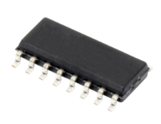
Analog Devices Inc.The ADG609 is a monolithic CMOS analog multiplexer comprising four differential channels. The ADG609 switches one of four differential inputs to a common differential output as determined by the 2-bit binary address lines A0 and A1. An EN input on both devices is used to enable or disable the device. When disabled, all channels are switched OFF.The ADG609 is designed on an enhanced LC2 MOS process which provides low power dissipation yet gives high switching speed and low on resistance. Each channel conducts equally well in both directions when ON and has an input signal range which extends to the supplies. In the OFF condition, signal levels up to the supplies are blocked. All channels exhibit break before make switching action preventing momentary shorting when switching channels. Inherent in the design is low charge injection for minimum transients when switching the digital inputs.
ADG712BRZ
Part Number : ADG712BRZ
Analog Devices Inc.The ADG712 is a monolithic CMOS device containing four independently selectable switches. It is designed on an advanced submicron process that provides low power dissipation yet gives high switching speed, low on resistance, low leakage currents and high bandwidth.The ADG712 operates from a single +1.8 V to +5.5 V supply, making it ideal for use in battery powered instruments and with the new generation of DACs and ADCs from Analog Devices. Fast switching times and high bandwidth make the part suitable for video signal switching.Each switch conducts equally well in both directions when ON. The ADG712 is available in 16-lead TSSOP and 16-lead SOIC packages.
ADL5541ACPZ-R7
Part Number : ADL5541ACPZ-R7
Analog Devices Inc.The ADL5541 is a broadband 15 dB linear amplifier that operates at frequencies up to 6 GHz. The device can be used in a wide variety of CATV, cellular, and instrumentation equipment. The ADL5541 provides a gain of 15 dB, which is stable over frequency, temperature, power supply, and from device to device. The device is internally matched to 50 Ω with an input return loss of 10 dB or better up to 6 GHz. Only input/output ac coupling capacitors, power supply decoupling capacitors, and an external inductor are required for operation. The ADL5541 is fabricated on an InGaP HBT process and has an ESD rating of 1 kV (Class 1C). The device is packaged in a 3 mm × 3 mm LFCSP that uses an exposed paddle for excellent thermal impedance. The ADL5541 consumes 90 mA on a single 5 V supply and is fully specified for operation from −40°C to +85°C. A fully populated RoHS-compliant evaluation board is available. The ADL5542 is a companion part that offers a gain of 20 dB in a pin-compatible package.
ADM1191-2ARMZ-R7
Part Number : ADM1191-2ARMZ-R7
Analog Devices Inc.The ADM1191 is an integrated current sense amplifier that offers digital current and voltage monitoring via an on-chip, 12-bit analog-to-digital converter (ADC), communicated through an I2C interface. An internal current sense amplifier senses voltage across the sense resistor in the power path via the VCC pin and the SENSE pin.A 12-bit ADC can measure the current seen in the sense resistor, as well as the supply voltage on the VCC pin.An industry-standard I2C interface allows a controller to read current and voltage data from the ADC. Measurements can be initiated by an I2C command or via the convert (CONV) pin. The CONV pin is especially useful for synchronizing reads on multiple ADM1191 devices. Alternatively, the ADC can run continuously, and the user can read the latest conversion data whenever it is required. Up to 16 unique I2C addresses can be created, depending on the way the A0 pin and the A1 pin are connected.A SETV pin is also included. A voltage applied to this pin is internally compared to the output voltage on the current sense amplifier. The output of the SETV comparator asserts when the current sense amplifier output exceeds the SETV voltage. When this event occurs, the ALERTB output asserts.The ALERTB output can be used as a flag to warn a micro-controller or field programmable gate array (FPGA) of an overcurrent condition. ALERTB outputs of multiple ADM1191 devices can be tied together and used as a combined alert.The ADM1191 is packaged in a 10-lead MSOP.APPLICATIONS Power monitoring/power budgeting Central office equipment Telecommunication and data communication equipment PCs/servers
ADM3232EARUZ
Part Number : ADM3232EARUZ
Analog Devices Inc.The ADM3232E transceiver is a high speed, 2-channel RS-232/V.28 interface device that operates from a single 3.3 V power supply. Low power consumption makes it ideal for battery-powered portable instruments. The ADM3232E conforms to the EIA-232E and CCITT V.28 specifications and operates at data rates up to 460 kbps.All RS-232 (TxOUT and RxIN) and TTL/CMOS (TxIN and RxOUT) inputs and outputs are protected against electrostatic discharges (up to ±15 kV ESD protection). This ensures compliance with IEC 1000-4-2 requirements.This device is ideally suited for operation in electrically harsh environments or where RS-232 cables are frequently plugged/ unplugged, with the ±15 kV ESD protection of the ADM3232E input/output pins.Emissions are also controlled to within very strict limits. CMOS technology is used to keep the power dissipation to an absolute minimum, allowing maximum battery life in portable applications.Four external 0.1 μF charge pump capacitors are used for the voltage doubler/inverter, permitting operation from a single 3.3 V supply.The ADM3232E is available in a 16-lead narrow SOIC package, as well as a space-saving 16-lead TSSOP.APPLICATIONS General-purpose RS-232 data link Portable instruments Handsets Industrial/telecom diagnostic ports
ADM483EARZ
Part Number : ADM483EARZ
Analog Devices Inc.The ADM483E is a 5 V, low power data transceiver with ±15 kV ESD protection suitable for half-duplex communication on multipoint bus transmission lines. The ADM483E is designed for balanced data transmission and complies with TIA/EIA Standards RS-485 and RS-422, which allow up to 32 transceivers on a bus.The ADM483E has a low current shutdown mode in which it consumes only 0.1 μA. Because only one driver is enabled at any time, the output of a disabled or power-down driver is three-stated to avoid overloading the bus. Drivers are short-circuit current-limited and are protected against excessive power dissipation by thermal shutdown circuitry that places their outputs into a high impedance state. The receiver input has a fail-safe feature that guarantees a logic high output if the input is open circuit. The ADM483E is fully specified over the industrial temperature ranges and is available in 8-lead SOIC_N packages. APPLICATIONS Low power RS-485 systems Electrically harsh environments EMI sensitive applications DTE-DCE interface Packet switching Local area networks
ADM705ANZ
Part Number : ADM705ANZ
Analog Devices Inc.The ADM705 / ADM706 / ADM707 / ADM708 microprocessorsupervisory circuits are suitable for monitoring 5 V powersupplies/batteries and microprocessor activity.The ADM705 / ADM706 provide power-supply monitoringcircuitry that generate a reset output during power-up, powerdown,and brownout conditions. The reset output remainsoperational with VCC as low as 1 V. Independent watchdogmonitoring circuitry is also provided. This is activated if thewatchdog input has not been toggled within 1.60 sec.In addition, there is a 1.25 V threshold detector to warn ofpower failures, to detect low battery conditions, or to monitor anadditional power supply. An active low, debounced manual resetinput (MR) is also included.The ADM705 and ADM706 are identical except for the resetthreshold monitor levels, which are 4.65 V and 4.40 V, respectively.The ADM707 and ADM708 provide a similar functionality tothe ADM705 and ADM706 and only differ in that a watchdogtimer function is not available. Instead, an active high resetoutput (RESET) is available as well as the active low reset output(RESET). The ADM707 and ADM708 are identical except forthe reset threshold monitor levels, which are 4.65 V and 4.40 V,respectively.All devices are available in narrow 8-lead PDIP and 8-lead SOICpackages.APPLICATIONS Microprocessor systems Computers Controllers Intelligent instruments Critical microprocessor supply monitoring
ADR363BUJZ-REEL7
Part Number : ADR363BUJZ-REEL7
Analog Devices Inc.The ADR360/ADR361/ADR363/ADR364/ADR365/ADR366 are precision 2.048 V, 2.500 V, 3.000 V, 4.096 V, 5.000 V, and 3.300 V band gap voltage references that offer low power and high precision in a compact TSOT package. Using proprietary temperature drift curvature correction techniques from Analog Devices, Inc., the ADR360/ADR361/ADR363/ADR364/ ADR365/ADR366 references achieve a low temperature drift of 9 ppm/°C in a TSOT package.The ADR360/ADR361/ADR363/ADR364/ADR365/ADR366 family of micropower, low dropout voltage references provide a stable output voltage from a minimum supply of 300 mV greater than the output. The advanced design of the devices eliminates the need for external capacitors, which further reduces board space and system cost. The combination of low power operation, small size, and ease of use makes the ADR360/ADR361/ADR363/ ADR364/ADR365/ADR366 precision voltage references ideally suited for battery-operated applications.See the Ordering Guide for automotive grades.Applications Battery-powered instruments Portable medical instruments Data acquisition systems Industrial process controls Automotive
ADR525ARTZ-REEL7
Part Number : ADR525ARTZ-REEL7
Analog Devices Inc.Designed for space-critical applications, the ADR525/ADR530/ ADR550 are high precision shunt voltage references, housed in ultrasmall SC70 and SOT-23-3 packages. These references feature low temperature drift of 40 ppm/°C, an initial accuracy of better than ±0.2%, and ultralow output noise of 18 μVP-P.Available in output voltages of 2.5 V, 3.0 V, and 5.0 V, the advanced design of the ADR525/ADR530/ADR550 eliminates the need for compensation by an external capacitor, yet the references are stable with any capacitive load. The minimum operating current increases from a mere 50 μA to a maximum of 15 mA. This low operating current and ease of use make these references ideally suited for handheld, battery-powered applications.A trim terminal is available on the ADR525/ADR530/ADR550 to allow adjustment of the output voltage over a ±0.5% range, without affecting the temperature coefficient of the device. This feature provides users with the flexibility to trim out small system errors.For better initial accuracy and wider temperature range, see the ADR5040/ADR5041/ADR5043ADR5044/ADR5045 family at www.analog.com.APPLICATIONS Portable, battery-powered equipment Automotive Power supplies Data acquisition systems Instrumentation and process control Energy measurement
ADSP-BF525ABCZ-5
Part Number : ADSP-BF525ABCZ-5
Analog Devices Inc.The ADSP-BF525 offers up to 600 MHz performance and up to 1200 MMACs. This processor core is supported by an advanced DMA controller supporting one-and two-dimensional DMA transfers between on-chip memory, off-chip memory, and system peripherals. The combination of the processor core speed and the DMA controller allows for efficient processing of audio, voice, video, and image data.The ADSP-BF525 provides peripheral flexibility to complement its high performance processing. The HS USB OTG host direct memory access (HDMA) and NAND flash controller are just a few of the peripheral options on the ADSP-BF525 family—not to mention the availability of up to 48 GPIO ports.For applications where product differentiation represents a challenge for securing market leadership, the ADSP-BF525 enables developers to provide features and benefits to augment their product offerings without compromising cost or power. The scalability of the ADSP-BF525 makes it an ideal candidate for Premium Audio Players where differentiation of features can be realized without sacrificing system cost. Where the diversity of Multimedia applications and content security are key attributes the ADSP-BF525 provides processing flexibility and Lockbox™ Secure Technology to enable users to develop freely and without bounds.IP protection has become a necessary part of today’s embedded computing applications. The ADSP-BF525 provides a security scheme which balances flexibility and upgradeability with performance through the inclusion of a firmware-based solution including OTP (One Time Programmable) memory to enable users to implement private keys for secure access to program code.
ADSP-BF525KBCZ-6A
Part Number : ADSP-BF525KBCZ-6A
Analog Devices Inc.The ADSP-BF525 offers up to 600 MHz performance and up to 1200 MMACs. This processor core is supported by an advanced DMA controller supporting one-and two-dimensional DMA transfers between on-chip memory, off-chip memory, and system peripherals. The combination of the processor core speed and the DMA controller allows for efficient processing of audio, voice, video, and image data.The ADSP-BF525 provides peripheral flexibility to complement its high performance processing. The HS USB OTG host direct memory access (HDMA) and NAND flash controller are just a few of the peripheral options on the ADSP-BF525 family—not to mention the availability of up to 48 GPIO ports.For applications where product differentiation represents a challenge for securing market leadership, the ADSP-BF525 enables developers to provide features and benefits to augment their product offerings without compromising cost or power. The scalability of the ADSP-BF525 makes it an ideal candidate for Premium Audio Players where differentiation of features can be realized without sacrificing system cost. Where the diversity of Multimedia applications and content security are key attributes the ADSP-BF525 provides processing flexibility and Lockbox™ Secure Technology to enable users to develop freely and without bounds.IP protection has become a necessary part of today’s embedded computing applications. The ADSP-BF525 provides a security scheme which balances flexibility and upgradeability with performance through the inclusion of a firmware-based solution including OTP (One Time Programmable) memory to enable users to implement private keys for secure access to program code.
ADSP-BF561SKBZ600
Part Number : ADSP-BF561SKBZ600
Analog Devices Inc.The Blackfin® Processor family expands the performance envelope with the ADSP-BF561. With two high performance Blackfin Processor cores, flexible cache architecture, enhanced DMA subsystem, and Dynamic Power Management (DPM) functionality, the ADSP-BF561 can support complex control and signal processing tasks while maintaining extremely high datathroughput.The ADSP-BF561 is a functional extension of the popular Blackfin Processor family and is ideally suited for a broad range of industrial, instrumentation, medical, and consumer appliance applications—allowing for scalability based upon the required data bandwidth and mix of control, plus signal processing needed in the end product.High-Level of Integration 328 KBytes of on-chip memory configured as: 32 KBytes of L1 instruction memory SRAM/Cache per core 64 KBytes of L1 data memory SRAM/Cache per core 4 KBytes of L1 scratchpad memory per core 128 KBytes of low-latency shared L2 memory 32-bit Memory Controller providing glueless connection to multiple banks of SDRAM, SRAM, Flash or ROM. Two Parallel Peripheral Interfaces Units supporting ITU-R 656 video data formats. Two dual-channel, full-duplex, synchronous serial ports supporting eight stereo I2S channels. Dual 16 Channel DMA Controllers, supporting one and two-dimension transfers. SPI-compatible Port. UART with support for IrDA®. 12 timer/counters supporting PWM, pulsewidth and event count modes. 48 Programmable Flags/General Purpose I/O. Event Handler. Dual Watchdog timers. PLL capable of 1x to 63x frequency multiplication. 256-ball Mini-BGA and 297-ball Sparse PBGA packages.
DC1009A-C
Part Number : DC1009A-C
Analog Devices Inc.The LTC2486 is a 4-channel (2-channel differential), 16-bit, No Latency ΔΣ™ ADC with Easy Drive™ technology. The patented sampling scheme eliminates dynamic input current errors and the shortcomings of on-chip buffering through automatic cancellation of differential input current. This allows large external source impedances and rail-to-rail input signals to be directly digitized while maintaining exceptional DC accuracy. The LTC2486 includes programmable gain, a high accuracy temperature sensor, and an integrated oscillator. This device can be configured to measure an external signal (from combinations of 4 analog input channels operating in single ended or differential modes) or its internal temperature sensor. It can be programmed to reject line frequencies of 50Hz, 60Hz, or simultaneous 50Hz/60Hz, provide a programmable gain from 1 to 256 in 8 steps, and configured to double its output rate. The integrated temperature sensor offers 1/2°C resolution and 2°C absolute accuracy. The LTC2486 allows a wide common mode input range (0V to VCC), independent of the reference voltage. Any combination of single-ended or differential inputs can be selected and the first conversion after a new channel selection is valid.Applications Direct Sensor Digitizer Direct Temperature Measurement Instrumentation Industrial Process Control
DC1010A-B
Part Number : DC1010A-B
Analog Devices Inc.The LTC2489 is a 4-channel (2-channel differential), 16-bit, No Latency ΔΣ™ ADC with Easy Drive technology and a 2-wire, I2C interface. The patented sampling scheme eliminates dynamic input current errors and the shortcomings of on-chip buffering through automatic cancellation of differential input current. This allows large external source impedances and rail-to-rail input signals to be directly digitized while maintaining exceptional DC accuracy. The LTC2489 includes an integrated oscillator. This device can be configured to measure an external signal from combinations of 4 analog input channels operating in single ended or differential modes. It automatically rejects line frequencies of 50Hz and 60Hz simultaneously. The LTC2489 allows a wide, common mode input range (0V to VCC), independent of the reference voltage. Any combination of single-ended or differential inputs can be selected and the first conversion, after a new channel is selected, is valid. Access to the multiplexer output enables optional external amplifiers to be shared between all analog inputs and auto calibration continuously removes their associated offset and drift.Applications Direct Sensor Digitizer Direct Temperature Measurement Instrumentation Industrial Process Control
DC1067A-A
Part Number : DC1067A-A
Analog Devices Inc.The LTC2450 is an ultra-tiny 16-bit analog-to-digital converter. The LTC2450 uses a single 2.7V to 5.5V supply, accepts a single-ended analog input voltage, and communicates through an SPI interface. It includes an integrated oscillator that does not require any external components. It uses a delta-sigma modulator as a converter core and provides single-cycle settling time for multiplexed applications. The converter is available in a 6-pin, 2mm × 2mm DFN package. The internal oscillator does not require any external components. The LTC2450 includes a proprietary input sampling scheme that reduces the average input sampling current several orders of magnitude.The LTC2450 is capable of up to 30 conversions per second and, due to the very large oversampling ratio, has extremely relaxed antialiasing requirements. The LTC2450 includes continuous internal offset and full-scale calibration algorithms which are transparent to the user, ensuring accuracy over time and over the operating temperature range. The converter uses its power supply voltage as the reference voltage and the single-ended, rail-to-rail input voltage range extends from GND to VCC.Following a conversion, the LTC2450 can automatically enter a sleep mode and reduce its power to less than 200nA. If the user samples the ADC once a second, the LTC2450 consumes an average of less than 50µW from a 2.7V supply.Applications System Monitoring Environmental Monitoring Direct Temperature Measurements Instrumentation Industrial Process Control Data Acquisition Embedded ADC Upgrades
DC1233A-B
Part Number : DC1233A-B
Analog Devices Inc.The LT5579 mixer is a high performance upconverting mixer optimized for frequencies in the 1.5GHz to 3.8GHz range. The single-ended LO input and RF output ports simplify board layout and reduce system cost. The mixer needs only –1dBm of LO power and the balanced design results in low LO signal leakage to the RF output. At 2.6GHz operation, the LT5579 provides high conversion gain of 1.3dB, high OIP3 of +26dBm and a low noise floor of –157.5dBm/Hz at a –5dBm RF output signal level. The LT5579 offers a high performance alternative to passive mixers. Unlike passive mixers, which have conversion loss and require high LO drive levels, the LT5579 delivers conversion gain at significantly lower LO input levels and is less sensitive to LO power level variations. The lower LO drive level requirements, combined with the excellent LO leakage performance, translate into lower LO signal contamination of the output signal.Applications GSM/EDGE, W-CDMA, UMTS, LTE and TD-SCDMA Basestations 2.6GHz and 3.5GHz WiMAX Basestations 2.4GHz ISM Band Transmitters High Performance Transmitters
DC1281A-A
Part Number : DC1281A-A
Analog Devices Inc.The LTC2209 is a 160Msps 16-bit A/D converter designed for digitizing high frequency, wide dynamic range signals with input frequencies up to 700MHz. The input range of the ADC can be optimized with the PGA front end.The LTC2209 is perfect for demanding communications applications, with AC performance that includes 77.3dBFS Noise Floor and 100dB spurious free dynamic range (SFDR). Ultra low jitter of 70fsRMS allows undersampling of high input frequencies with excellent noise performance. Maximum DC specs include ±5.5LSB INL, ±1LSB DNL (no missing codes).The digital output can be either differential LVDS or single-ended CMOS. There are two format options for the CMOS outputs: a single bus running at the full data rate or demultiplexed busses running at half data rate. A separate output power supply allows the CMOS output swing to range from 0.5V to 3.6V.The ENC+ and ENC– inputs may be driven differentially or single-ended with a sine wave, PECL, LVDS, TTL or CMOS inputs. An optional clock duty cycle stabilizer allows high performance at full speed with a wide range of clock duty cycles.Applications Telecommunications Receivers Cellular Base Stations Spectrum Analysis Imaging Systems
HMC496LP3
Part Number : HMC496LP3
Analog Devices Inc.The HMC496LP3(E) is a low noise Wideband Direct Quadrature Modulator RFIC which are ideal for digital modulation applications from 4 - 7 GHz including; WLL, U-NII, WLAN & microwave radios. Housed in a compact 3x3 mm (LP3) SMT QFN package, the RFIC requires minimal external components & provides a low cost alternative to more complicated double upconversion architectures.The RF output port is matched to 50 Ohms with no external components. The LO requires -3 to +6 dBm and can be driven in either differential or single-ended mode while the Baseband inputs will support modulation inputs from DC - 250 MHz typical. This device is optimized for a supply voltage of +3V @ 93 mA and will provide stable performance over a +2.7V to +3.3V range.Applications Fixed Wireless or WLL U-NII Radios 802.11a & HiperLAN WLAN C-band Microwave Radios
HMC593LP3E
Part Number : HMC593LP3E
Analog Devices Inc.The HMC593LP3 / HMC593LP3E are versatile, high dynamic range GaAs MMIC Low Noise Amplifiers that integrate a low loss LNA bypass mode on the IC. The amplifier is ideal for WiBro & WiMAX receivers operating between 3.3 and 3.8 GHz and provides 1.2 dB noise figure, 19 dB of gain and +29 dBm IP3 from a single supply of +5V @ 40mA.Input and output return losses are 23 and 13 dB respectively with no external matching components required. A single control line (0/+3V) is used to switch between LNA mode and a low 2 dB loss bypass mode reducing the current consumption to 10 A.Applications Wireless Infrastructure Fixed Wireless WiMAX & WiBro Tower Mounted Amplifiers
HMC615LP4E
Part Number : HMC615LP4E
Analog Devices Inc.The HMC615LP4(E) is a high linearity, GaAs FET converter IC that operates from 2.3 to 4.0 GHz and deliver a +35 dBm input third order intercept point. The LO amplifier output and high dynamic range mixer input are positioned so that an external LO filter can be placed in series between them.The IC operates from a single +5V supply consuming 65 mA of current and accepts a LO drive level of -2 to +6 dBm. The design requires no external baluns and supports IF frequencies between DC and 1 GHz. The HMC615LP4(E) is pin for pin compatible with the HMC551LP4(E), HMC552LP4(E) and HMC215LP4(E), which operate from 0.8 to 4 GHz.Applications PCS / 3G Infrastructure Base Stations & Repeaters WiMAX & WiBro ISM & Fixed Wireless


