ADR3430ARJZ-R2
Part Number : ADR3430ARJZ-R2
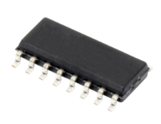
Analog Devices Inc.The ADR3412 / ADR3420 / ADR3425 / ADR3430 / ADR3433 / ADR3440 / ADR3450 are low-cost, low-power, high precision voltage references, featuring ± 0.1% initial accuracy, low operating current and low output noise in a small SOT23 package. For high accuracy, output voltage and temperature coefficient are trimmed digitally during final assembly using Analog Devices’ proprietary Digi-Trim® technology. Stability and reliability are further improved by the devices’ low output voltage hysteresis and low long-term output voltage drift.Furthermore, the low operating current of the device (100 μA max) facilitates usage in low-power devices, while its low output noise helps maintain signal integrity in critical signal processing systems.These CMOS are available in a wide range of output voltages, all of which are specified over the industrial temperature range of −40°C to +125 °C.APPLICATIONS Precision data acquisition systems Industrial instrumentation Medical devices Battery-powered devices
ADUM3473CRSZ
Part Number : ADUM3473CRSZ
Analog Devices Inc.The ADuM3470 / ADuM3471/ADuM3472 / ADuM3473 / ADuM3474 devicesare quad-channel, digital isolators withan integrated PWM controller and transformer driver for anisolated DC/DC converter. Based on the Analog Devices, Inc.,iCoupler® technology, the DC/DC converter provides up to 2 Wof regulated, isolated power at 3.3 V to 24 V from a 5.0 V inputsupply or from a 3.3 V supply. This eliminates the need for aseparate, isolated DC/DC converter in 2 W isolated designs.The iCoupler chip-scale transformer technology is used to isolatethe logic signals, and the integrated transformer driver withisolated secondary side control provides higher efficiency for theisolated DC/DC converter. The result is a small form factor, totalisolation solution.The ADuM347x isolators provide four independent isolationchannels in a variety of channel configurations and data rates.APPLICATIONS RS-232/RS-422/RS-485 transceivers Industrial field bus isolation Power supply startup bias and gate drives Isolated sensor interfaces Process controls Automotive
ADUM4400ARWZ
Part Number : ADUM4400ARWZ
Analog Devices Inc.The ADuM440x are 4-channel digital isolators based on the Analog Devices, Inc., iCoupler® technology. Combining high speed CMOS and monolithic air core transformer technology, these isolation components provide outstanding performance characteristics that are superior to the alternatives, such as optocoupler devices and other integrated couplers.The ADuM440x isolators provide four independent isolation channels in a variety of channel configurations and data rates (see the Ordering Guide). All models operate with the supply voltage on either side ranging from 3.0 V to 5.5 V, providing compatibility with lower voltage systems as well as enabling a voltage translation functionality across the isolation barrier. The ADuM440x isolators have a patented refresh feature that ensures dc correctness in the absence of input logic transitions and during power-up/power-down conditions.This family of isolators, like many Analog Devices isolators, offers very low power consumption, consuming one-tenth to one-sixth the power of comparable isolators at comparable data rates up to 10 Mbps. All models of the ADuM440x provide low pulse width distortion (
ADUM6202ARWZ
Part Number : ADUM6202ARWZ
Analog Devices Inc.The ADuM6200 / ADuM6201/ADuM6202 are dual-channel digital isolators with isoPower®, an integrated, isolated DC/DC converter. Based on the Analog Devices, Inc., iCoupler® technology, the DC/DC converter provides up to 400 mW of regulated, isolated power at either 5.0 V or 3.3 V from a 5.0 V input supply, or at 3.3 V from a 3.3 V supply at the power levels shown in Table 1 on the data sheet. These devices eliminate the need for a separate, isolated DC/DC converter in low power, isolated designs. The iCoupler chip scale transformer technology is used to isolate the logic signals and for the magnetic components of the DC/DC converter. The result is a small form factor, total isolation solution.The ADuM6200 / ADuM6201/ADuM6202 isolators provide two independent isolation channels in a variety of channel configurations and data rates (see the Ordering Guide for more information).isoPower uses high frequency switching elements to transfer power through its transformer. Special care must be taken during printed circuit board (PCB) layout to meet emissions standards. See the AN-0971 Application Note for board layout recommendations.APPLICATIONS RS-232/RS-422/RS-485 transceivers Industrial field bus isolation Power supply start-up bias and gate drives Isolated sensor interfaces Industrial PLCs
ADUM6404ARIZ
Part Number : ADUM6404ARIZ
Analog Devices Inc.The ADuM640x devices are quad-channel digital isolators with isoPower®, an integrated, isolated DC/DC converter. Based on the Analog Devices, Inc., iCoupler® technology, the DC/DC converter provides up to 500 mW of regulated, isolated power at either 5.0 V or 3.3 V from a 5.0 V input supply, or 3.3 V from a 3.3 V supply at the power levels shown in Table 1. This eliminates the need for a separate, isolated DC/DC converter in low power, isolated designs. The iCoupler chip scale transformer technology is used to isolate the logic signals and for the magnetic components of the DC/DC converter. The result is a small form factor, total isolation solution.The ADuM640x isolators provide four independent isolation channels in a variety of channel configurations and data rates (see the Ordering Guide for more information).isoPower uses high frequency switching elements to transfer power through its transformer. Special care must be taken during printed circuit board (PCB) layout to meet emissions standards. Refer to the AN-0971 application note for board layout recommendations at www.analog.com.
ADXL346ACCZ-RL
Part Number : ADXL346ACCZ-RL
Analog Devices Inc.The ADXL346 is a small, thin, ultralow power, 3-axis accelerometer with high resolution (13-bit) measurement at up to ±16g. Digital output data is formatted as 16-bit twos complement and is accessible through either an SPI (3- or 4-wire) or I2C® digital interface.The ADXL346 is well suited for mobile device applications. It measures the static acceleration of gravity in tilt-sensing applications, as well as dynamic acceleration resulting from motion or shock. Its high resolution (4 mg/LSB) enables measurement of inclination changes of less than 1.0°.Several special sensing functions are provided. Activity and inactivity sensing detect the presence or lack of motion by comparing the acceleration on any axis with user-set thresholds. Tap sensing detects single and double taps in any direction. Free-fall sensing detects if the device is falling. Orientation detection is capable of concurrent four- and six-position sensing and a user-selectable interrupt on orientation change for 2D or 3D applications. These functions can be mapped individually to either of two interrupt output pins. An integrated, patent pending memory management system with 32-level first in, first out (FIFO) buffer can be used to store data to minimize host processor activity and lower overall system power consumption.Low power modes enable intelligent motion-based power management with threshold sensing and active acceleration measurement at extremely low power dissipation.The ADXL346 is supplied in a small, thin, 3 mm × 3 mm × 0.95 mm, 16-lead, plastic package.APPLICATIONS Handsets Medical instrumentation Gaming and pointing devices Industrial instrumentation Personal navigation devices Hard disk drive (HDD) protection
ADXRS453BEYZ
Part Number : ADXRS453BEYZ
Analog Devices Inc.The ADXRS453 is an angular rate sensor (gyroscope) intended for industrial, instrumentation, and stabilization applications in high vibration environments. An advanced, differential, quad sensor design rejects the influence of linear acceleration, enabling the ADXRS453 to offer high accuracy rate sensing in harsh envi-ronments where shock and vibration are present.The ADXRS453 uses an internal, continuous self-test architec-ture. The integrity of the electromechanical system is checked by applying a high frequency electrostatic force to the sense structure to generate a rate signal that can be differentiated from the base-band rate data and internally analyzed.The ADXRS453 is capable of sensing an angular rate of up to ±300°/sec. Angular rate data is presented as a 16-bit word that is part of a 32-bit SPI message.The ADXRS453 is available in a 16-lead plastic cavity SOIC (SOIC_CAV) and an SMT-compatible vertical mount package (LCC_V), and is capable of operating across a wide voltage range (3.3 V to 5 V). ApplicationsRotation sensing in high vibration environments Rotation sensing for industrial and instrumentation applicationsHigh performance platform stabilization
ADXRS623BBGZ
Part Number : ADXRS623BBGZ
Analog Devices Inc.The ADXRS623 is a complete angular rate sensor (gyroscope)that uses the Analog Devices, Inc. surface-micromachiningprocess to create a functionally complete and low cost angularrate sensor integrated with all required electronics on one chip.The manufacturing technique for this device is the same highvolume BiMOS process used for high reliability automotiveairbag accelerometers.The ADXRS623 is an automotive grade gyroscope. Automotive grade gyroscopes have more extensive guaranteed min/max specifications due to automotive testing.The output signal, RATEOUT (1B, 2A), is a voltageproportional to the angular rate about the axis that is normal tothe top surface of the package. The output is ratiometric withrespect to a provided reference supply. A single externalresistor between SUMJ and RATEOUT can be used to lowerthe scale factor. An external capacitor sets the bandwidth. Otherexternal capacitors are required for operation.A temperature output is provided for compensation techniques.Two digital self-test inputs electromechanically excite thesensor to test proper operation of both the sensor and the signalconditioning circuits. The ADXRS623 is available in a 7 mm ×7 mm × 3 mm BGA chip scale package.APPLICATIONS Inertial measurement units Platform stabilization Robotics
DC1501A-B
Part Number : DC1501A-B
Analog Devices Inc.The LTC2392-16 is a low noise, high speed 16-bit successive approximation register (SAR) ADC. Operating from a single 5V supply, the LTC2392-16 supports a large ±4.096V fully differential input range, making it ideal for high performance applications which require maximum dynamic range. The LTC2392-16 achieves ±2LSB INL max, no missing codes at 16-bits and 94dB SNR (typ). The LTC2392-16 includes a precision internal reference with a guaranteed 0.5% initial accuracy and a ±20ppm/°C (max) temperature coefficient. Fast 500ksps throughput with no cycle latency in both parallel and serial interface modes makes the LTC2392-16 ideally suited for a wide variety of high speed applications. An internal oscillator sets the conversion time, easing external timing considerations. The LTC2392-16 dissipates only 110mW at 500ksps, while both nap and sleep power-down modes are provided to further reduce power during inactive periods.Applications Medical Imaging High Speed Data Acquisition Digital Signal Processing Industrial Process Control Instrumentation ATE
DC1532A-B
Part Number : DC1532A-B
Analog Devices Inc.The LTC2268-14/LTC2267-14/LTC2266-14 are 2-channel, simultaneous sampling 14-bit A/D converters designed for digitizing high frequency, wide dynamic range signals. They are perfect for demanding communications applications with AC performance that includes 73.1dB SNR and 88dB spurious free dynamic range (SFDR). Ultralow jitter of 0.15psRMS allows undersampling of IF frequencies with excellent noise performance.DC specs include ±1LSB INL (typ), ±0.3LSB DNL (typ) and no missing codes over temperature. The transition noise is a low 1.2LSBRMS. The digital outputs are serial LVDS to minimize the number of data lines. Each channel outputs two bits at a time (2-lane mode). At lower sampling rates there is a one bit per channel option (1-lane mode). The LVDS drivers have optional internal termination and adjustable output levels to ensure clean signal integrity. The ENC+ and ENC– inputs may be driven differentially or single-ended with a sine wave, PECL, LVDS, TTL, or CMOS inputs. An internal clock duty cycle stabilizer allows high performance at full speed for a wide range of clock duty cycles. Bits LTC2267-12 12 LTC2267-14 14 Applications Communications Cellular Base Stations Software Defined Radios Portable Medical Imaging Multichannel Data Acquisition Nondestructive Testing
DC1554A-A
Part Number : DC1554A-A
Analog Devices Inc.The LTM2882 is a complete galvanically isolated dual RS232 μModule® (micromodule) transceiver. No external components are required. A single 3.3V or 5V supply powers both sides of the interface through an integrated, isolated DC/DC converter. A logic supply pin allows easy interfacing with different logic levels from 1.62V to 5.5V, independent of the main supply.Coupled inductors and an isolation power transformer provide 2500VRMS of isolation between the line transceiver and the logic interface. This device is ideal for systems with different grounds, allowing for large common mode voltages. Uninterrupted communication is guaranteed for common mode transients greater than 30kV/μs.This part is compatible with the TIA/EIA-232-F standard. Driver outputs are protected from overload and can be shorted to ground or up to ±15V without damage. An auxiliary isolated digital channel is available. This channel allows configuration for half-duplex operation by controlling the DE pin.Enhanced ESD protection allows this part to withstand up to ±10kV (human body model) on the transceiver interface pins to isolated supplies and across the isolation barrier to logic supplies without latch-up or damage.Applications Isolated RS232 Interface Industrial Communication Test and Measurement Equipment Breaking RS232 Ground Loops
DC1561B
Part Number : DC1561B
Analog Devices Inc.The LTC4278 is an integrated Powered Device (PD) controller and switching regulator intended for high power IEEE 802.3at and 802.3af applications. With a wide input voltage range, the LTC4278 is specifically designed to support PD applications that include a low-voltage auxiliary power input such as a 12V wall adaptor. The inclusion of a shutdown pin provides simple implementation of both PoE and auxiliary dominate applications. In addition, the LTC4278 supports both 1-event and 2-event classifications as defined by the IEEE, thereby allowing the use in a wide range of product configurations.The LTC4278 synchronous, current mode, flyback controller generates multiple supply rails in a single conversion step providing for the highest system efficiency while maintaining tight regulation across all outputs. The LTC4278 includes Linear Technology’s patented No-Opto feedback topology to provide full IEEE 802.3 isolation without the need of an opto-isolator circuit. A true soft-start function allows graceful ramp-up of all output voltages.The LTC4278 is available in a space saving 32-pin DFN package.Applications VoIP Phones with Advanced Display Options Dual-Radio Wireless Access Points PTZ Security Cameras RFID Readers Industrial Controls
DC1703A-D
Part Number : DC1703A-D
Analog Devices Inc.The LTC2655 is a family of Quad I2C 16-/12-Bit Rail-to-Rail DACs with integrated 10ppm/°C max reference. The DACs have built-in high performance, rail-to-rail, output buffers and are guaranteed monotonic. The LTC2655-L has a full-scale output of 2.5V with the integrated reference and operates from a single 2.7V to 5.5V supply. The LTC2655-H has a full-scale output of 4.096V with the integrated reference and operates from a 4.5V to 5.5V supply. Each DAC can also operate with an external reference, which sets the full-scale output to 2 times the external reference voltage.The parts use the 2-wire I2C compatible serial interface. The LTC2655 operates in both the standard mode (maximum clock rate of 100kHz) and the fast mode (maximum clock rate of 400kHz). The LTC2655 incorporates a power-on reset circuit that is controlled by the PORSEL pin. If PORSEL is tied to GND the DACs power-on reset to zero-scale. If PORSEL is tied to VCC, the DACs power-on reset to mid-scale.Applications Mobile Communications Process Control and Industrial Automation Instrumentation Automatic Test Equipment Automotive
DC996B-C
Part Number : DC996B-C
Analog Devices Inc.The LTC2208-14 is a 130Msps, sampling 14-bit A/D converter designed for digitizing high frequency, wide dynamic range signals with input frequencies up to 700MHz. The input range of the ADC can be optimized with the PGA front end.The LTC2208-14 is perfect for demanding communications applications, with AC performance that includes 77.1dBFS Noise Floor and 98dB spurious free dynamic range (SFDR). Ultralow jitter of 70fsRMS allows undersampling of high input frequencies with excellent noise performance. Maximum DC specs include ±1.5LSB INL, ±0.5LSB DNL (no missing codes).The digital output can be either differential LVDS or single-ended CMOS. There are two format options for the CMOS outputs: a single bus running at the full data rate or demultiplexed buses running at half data rate. A separate output power supply allows the CMOS output swing to range from 0.5V to 3.6V.The ENC+ and ENC– inputs may be driven differentially or single-ended with a sine wave, PECL, LVDS, TTL or CMOS inputs. An optional clock duty cycle stabilizer allows high performance at full speed with a wide range of clock duty cycles. Bits LTC2208-14 14 LTC2208-16 16 Applications Telecommunications Receivers Cellular Base Stations Spectrum Analysis Imaging Systems ATE
AD8421BRMZ-RL
Part Number : AD8421BRMZ-RL
Analog Devices Inc.The AD8421 is a low cost, low power, extremely low noise, ultralow bias current, high speed instrumentation amplifier that is ideally suited for a broad spectrum of signal conditioning and data acquisition applications. This product features extremely high CMRR, allowing it to extract low level signals in the presence of high frequency common-mode noise over a wide temperature range. The 10 MHz bandwidth, 35 V/µs slew rate, and 0.6 µs settling time to 0.001% (G = 10) allow the AD8421 to amplify high speed signals and excel in applications that require high channel count, multiplexed systems. Even at higher gains, the current feedback architecture maintains high performance; for example, at G = 100, the bandwidth is 2 MHz and the settling time is 0.8 µs. The AD8421 has excellent distortion performance, making it suitable for use in demanding applications such as vibration analysis. The AD8421 delivers industry-leading 3 nV/√Hz input voltage noise and 200 fA/√Hz current noise with only 2 mA quiescent current, making it an ideal choice for measuring low level signals. For applications with high source impedance, the AD8421 employs innovative process technology and design techniques to provide noise performance that is limited only by the sensor. The AD8421 uses unique protection methods to ensure robust inputs while still maintaining very low noise. This protection allows input voltages up to 40 V from the opposite supply rail without damage to the part. A single resistor sets gains between 1 and 10,000. The reference pin can be used to apply a precise offset to the output voltage.The AD8421 performance is specified from −40°C to +85°C for the 8-lead MSOP and SOIC packages, and from −40°C to 125°C for the 8-lead LFCSP package.Applications Medical instrumentation Precision data acquisition Microphone preamplification Vibration analysis Multiplexed input applications ADC driver
AD8451ASTZ
Part Number : AD8451ASTZ
Analog Devices Inc.The AD8451 is a precision analog front end and controller for testing and monitoring battery cells. A precision fixed gain instrumentation amplifier (IA) measures the battery charge/discharge current, and a fixed gain difference amplifier (DA) measures the battery voltage. Internal laser trimmed resistor networks set the gains for the IA and the DA, optimizing the performance of the AD8451 over the rated temperature range. The IA gain is 26 and the DA gain is 0.8 V/V.Voltages at the ISET and VSET inputs set the desired constant current (CC) and constant voltage (CV) values. CC to CV switching is automatic and transparent to the system.A TTL logic level input, MODE, selects the charge or discharge mode (high for charge, low for discharge). An analog output, VCTRL, interfaces directly with the Analog Devices, Inc., ADP1972 PWM controller.The AD8451 simplifies designs by providing excellent accuracy, performance over temperature, flexibility with functionality, and overall reliability in a space-saving package. The AD8451 is available in an 80-lead, 14 mm × 14 mm × 1 mm LQFP package and is rated for an operating temperature of −40°C to +85°C.APPLICATIONS Battery cell formation and testing Battery module testing
AD9253-125EBZ
Part Number : AD9253-125EBZ
Analog Devices Inc.The AD9253 is a quad, 14-bit, 80 MSPS/105 MSPS/125 MSPSanalog-to-digital converter (ADC) with an on-chip sample-and-holdcircuit designed for low cost, low power, small size,and ease of use. The product operates at a conversion rate ofup to 125 MSPS and is optimized for outstanding dynamicperformance and low power in applications where a smallpackage size is critical.The ADC requires a single 1.8 V power supply and LVPECL-/CMOS-/LVDS-compatible sample rate clock for full performanceoperation. No external reference or driver components arerequired for many applications.The ADC automatically multiplies the sample rate clock for theappropriate LVDS serial data rate. A data clock output (DCO) forcapturing data on the output and a frame clock output (FCO)for signaling a new output byte are provided. Individual-channelpower-down is supported and typically consumes less than 2 mWwhen all channels are disabled. The ADC contains several featuresdesigned to maximize flexibility and minimize system cost, such as programmable output clock and data alignment and digitaltest pattern generation. The available digital test patternsinclude built-in deterministic and pseudorandom patterns, alongwith custom user-defined test patterns entered via the serial portinterface (SPI).The AD9253 is available in a RoHS-compliant, 48-lead LFCSP.It is specified over the industrial temperature range of −40°C to+85°C. This product is protected by a U.S. patent.PRODUCT HIGHLIGHTS Small Footprint. Four ADCs are contained in a small, spacesaving package. Low power of 110 mW/channel at 125 MSPS with scalable power options. Pin compatible to the AD9633 12-bit quad ADC. Ease of Use. A data clock output (DCO) operates at frequencies of up to 500 MHz and supports double data rate (DDR) operation. User Flexibility. The SPI control offers a wide range of flexible features to meet specific system requirementsAPPLICATIONS Medical ultrasound High speed imaging Quadrature and diversity radio receivers Test equipment
AD9364BBCZREEL
Part Number : AD9364BBCZREEL
Analog Devices Inc.The AD9364 is a 1 x 1 channel high performance, highly integrated RF Agile Transceiver™. Its programmability and wideband capability make it ideal for a broad range of transceiver applications. The device combines an RF front end with a flexible mixed-signal baseband section and integrated frequency synthesizers, simplifying design-in by providing a configurable digital interface to a processor. The AD9364 operates in the 70 MHz to 6.0 GHz range, covering most licensed and unlicensed bands. Channel bandwidths from less than 200 kHz to 56 MHz are supported.The AD9364 is packaged in a 10 mm × 10 mm, 144-ball chip scale package ball grid array (CSP_BGA).Applications Point to point communication systems Femtocell/picocell/microcell base stations General-purpose radio systems
AD9434BCPZ-370
Part Number : AD9434BCPZ-370
Analog Devices Inc.The AD9434 is a 12-bit monolithic sampling analog-to-digital converter (ADC) optimized for high performance, low power, and ease of use. The part operates at up to a 500 MSPS conversion rate and is optimized for outstanding dynamic performance in wideband carrier and broadband systems. All necessary functions, including a sample-and-hold and voltagereference, are included on the chip to provide a complete signal conversion solution. The VREF pin can be used to monitor the internal reference or provide an external voltage reference (external reference mode must be enabled through the SPI port). The ADC requires a 1.8 V analog voltage supply and a differential clock for full performance operation. The digital outputs are LVDS (ANSI-644) compatible and support twos complement, offset binary format, or Gray code. A data clock output is available for proper output data timing.Fabricated on an advanced BiCMOS process, the AD9434 isavailable in a 56-lead LFCSP, specified over the industrial temperature range (−40°C to +85°C). This part is protected under a U.S. patent.APPLICATIONS Wireless and wired broadband communications Cable reverse path Communications test equipment Radar and satellite subsystems Power amplifier linearizationPRODUCT HIGHLIGHTS High Performance. Maintains 65 dBFS SNR at 500 MSPS with a 250 MHz input. Low Power. Consumes only 660 mW at 500 MSPS. Ease of Use. LVDS output data and output clock signal allow interface to current FPGA technology. The on-chip reference and sample and hold provide flexibility in system design. Use of a single 1.8 V supply simplifies system power supply design. Serial Port Control. Standard serial port interface supports various product functions, such as data formatting, power-down, gain adjust, and output test pattern generation. The AD9434 is pin compatible with the AD9230, and can be substituted in many applications with minimal design changes.
AD9613BCPZ-250
Part Number : AD9613BCPZ-250
Analog Devices Inc.The AD9613 is a dual 12-bit, analog-to-digital converter (ADC) with sampling speeds up to 250 MSPS. The AD9613 is designed to support communications applications where low cost, small size, wide bandwidth and versatility are desired.The dual ADC core features a multistage, differential pipelinedarchitecture with integrated output error correction logic. EachADC features wide bandwidth inputs supporting a variety of user-selectable input ranges. An integrated voltage reference eases design considerations. A duty cycle stabilizer is provided to compensate for variations in the ADC clock duty cycle, allowing the converters to maintain excellent performance.The ADC output data are routed directly to the two external 12-bit LVDS output ports and formatted either as interleaved or channel multiplexed.Flexible power-down options allow significant power savings,when desired.Programming for setup and control are accomplished using a 3-wire SPI-compatible serial interface.The AD9613 is available in a 64-lead LFCSP and is specified overthe industrial temperature range of −40°C to +85°C.PRODUCT HIGHLIGHTS Integrated dual, 12-bit, 170 MSPS/210 MSPS/250 MSPS ADCs. Fast overrange and threshold detect. Proprietary differential input maintains excellent SNR performance for input frequencies up to 400 MHz. SYNC input allows synchronization of multiple devices. 3-pin, 1.8V SPI port for register programming and register readback. Pin compatibility with the AD9643, allowing a simple migration up to 14 bits, and with the AD6649 and the AD6643.APPLICATIONS Communications Diversity radio systems Multimode digital receivers (3G) TD-SCDMA, WiMax, WCDMA, CDMA2000, GSM, EDGE, LTE I/Q demodulation systems Smart antenna systems General-purpose software radios Ultrasound equipment Broadband data applications


