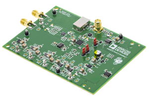
AD9628BCPZ-105
Part Number : AD9628BCPZ-105
Analog Devices Inc.The AD9628 is a monolithic, dual-channel, 1.8 V supply, 12-bit, 125 MSPS/105 MSPS analog-to-digital converter (ADC). It features a high performance sample-and-hold circuit and on-chip voltage reference.The product uses multistage differential pipeline architecture with output error correction logic to provide 12-bit accuracy at 125 MSPS data rates and to guarantee no missing codes over the full operating temperature range.The ADC contains several features designed to maximize flexibility and minimize system cost, such as programmable clock and data alignment and programmable digital test pattern generation. The available digital test patterns include built-in deterministic and pseudorandom patterns, along with custom user-defined test patterns entered via the serial port interface (SPI).A differential clock input controls all internal conversion cycles. An optional duty cycle stabilizer (DCS) compensates for wide variations in the clock duty cycle while maintaining excellent overall ADC performance.The digital output data is presented in offset binary, Gray code, or twos complement format. A data output clock (DCO) is provided for each ADC channel to ensure proper latch timing with receiving logic. 1.8 V CMOS or LVDS output logic levels are supported. Output data can also be multiplexed onto a single output bus.APPLICATIONS Communications Diversity radio systems Multimode digital receivers GSM, EDGE, W-CDMA, LTE, CDMA2000, WIMAX, TD-SCDMA I/Q demodulation systems Smart antenna systems Broadband data applications Battery-powered instruments Hand-held scope meters Portable medical imaging Ultrasound Radar/LIDARPRODUCT HIGHLIGHTS The AD9628 operates from a single 1.8 V analog power supply and features a separate digital output driver supply to accommodate 1.8 V CMOS or LVDS logic families. The patented sample-and-hold circuit maintains excellent performance for input frequencies up to 200 MHz and is designed for low cost, low power, and ease of use. A standard serial port interface supports various product features and functions, such as data output formatting, internal clock divider, power-down, DCO/data timing and offset adjustments. The AD9628 is packaged in a 64-lead RoHS-compliant LFCSP that is pin compatible with the AD9650 / AD9269 / AD9268 16-bit ADC, the AD9258 / AD9251 / AD9648 14-bit ADCs, the AD9231 12-bit ADC, and the AD9608 / AD9204 10-bit ADCs, enabling a simple migration path between 10-bit and 16-bit converters sampling from 20MSPS to 125MSPS.
AD9637BCPZ-40
Part Number : AD9637BCPZ-40
Analog Devices Inc.The AD9637 is an octal, 12-bit, 40/80 MSPS analog-to-digital converter (ADC) with an on-chip sample-and-hold circuit designed for low cost, low power, small size, and ease of use. The product operates at a conversion rate of up to 80 MSPS and is optimized for outstanding dynamic performance and low power in applications where a small package size is critical.The ADC requires a single 1.8 V power supply and LVPECL-/ CMOS-/LVDS-compatible sample rate clock for full performance operation. No external reference or driver components are required for many applications.The ADC automatically multiplies the sample rate clock for the appropriate LVDS serial data rate. A data clock output (DCO) for capturing data on the output and a frame clock output (FCO) for signaling a new output byte are provided. Individual channel power-down is supported and typically consumes less than 2 mW when all channels are disabled.The ADC contains several features designed to maximize flexibility and minimize system cost, such as programmable clock and data alignment and programmable digital test pattern generation. The available digital test patterns include built-in deterministic and pseudorandom patterns, along with custom user-defined test patterns entered via the serial port interface (SPI).The AD9637 is available in a RoHS-compliant, 64-lead LFCSP. It is specified over the industrial temperature range of −40°C to +85°C. This product is protected by a U.S. patent.APPLICATIONS Medical imaging and nondestructive ultrasound Portable ultrasound and digital beam-forming systems Quadrature radio receivers Diversity radio receivers Optical networking Test equipmentPRODUCT HIGHLIGHTS Small Footprint. Eight ADCs are contained in a small, space-saving package. Low Power of 60 mW/Channel at 80 MSPS with Scalable Power Options. Ease of Use. A data clock output (DCO) is provided that operates at frequencies of up to 480 MHz and supports double data rate (DDR) operation. User Flexibility. The SPI control offers a wide range of flexible features to meet specific system requirements. Pin Compatible with the AD9257 (14-Bit Octal ADC).
AD9837BCPZ-RL
Part Number : AD9837BCPZ-RL
Analog Devices Inc.The AD9837 is a low power, programmable waveform generatorcapable of producing sine, triangular, and square wave outputs.Waveform generation is required in various types of sensing,actuation, and time domain reflectometry (TDR) applications. The outputfrequency and phase are software programmable, allowing easytuning. The frequency registers are 28 bits: with a 16 MHz clock rate, resolution of 0.06 Hz can be achieved; with a 5 MHz clock rate, the AD9837can be tuned to 0.02 Hz resolution.The AD9837 is written to via a 3-wire serial interface. This serialinterface operates at clock rates up to 40 MHz and is compatiblewith DSP and microcontroller standards. The device operateswith a power supply from 2.3 V to 5.5 V.The AD9837 has a power-down (SLEEP) function. Sections of the device that are not being used can be powered down to minimize the current consumption of the part. For example, the DAC can be powered down when a clock output is being generated.The AD9837 is available in a 10-lead LFCSP_WD package.APPLICATIONS Frequency stimulus/waveform generation Liquid and gas flow measurement Sensory applications: proximity, motion, and defect detection Line loss/attenuation Test and medical equipment Sweep/clock generators Time domain reflectometry (TDR) applications
ADA4084-2ARZ-R7
Part Number : ADA4084-2ARZ-R7
Analog Devices Inc.The ADA4084-1 (single), ADA4084-2 (dual), and ADA4084-4 (quad) are single-supply, 10 MHz bandwidth amplifiers featuring rail-to-rail inputs and outputs. They are guaranteed to operate from +3 V to +30 V (or ±1.5 V to ±15 V).These amplifiers are well suited for single-supply applications requiring both ac and precision dc performance. The combination of wide bandwidth, low noise, and precision makes the ADA4084-1/ADA4084-2/ADA4084-4 useful in a wide variety of applications, including filters and instrumentation.Other applications for these amplifiers include portable telecommunications equipment, power supply control and protection, and use as amplifiers or buffers for transducers with wide output ranges. Sensors requiring a rail-to-rail input amplifier include Hall effect, piezoelectric, and resistive transducers.The ability to swing rail to rail at both the input and output enables designers to build multistage filters in single-supply systems and to maintain high signal-to-noise ratios.The ADA4084-1/ADA4084-2/ADA4084-4 are specified over the industrial temperature range of −40°C to +125°C.The single ADA4084-1 is available in the 5-lead SOT-23 and 8-lead SOIC; the dual ADA4084-2 is available in the 8-lead SOIC, 8-lead MSOP, and 8-lead LFCSP surface-mount packages; and the ADA4084-4 is offered in the 14-lead TSSOP and 16-lead LFCSP.The ADA4084-1/ADA4084-2/ADA4084-4 are members of a growing series of high voltage, low noise op amps offered by Analog Devices, Inc.Applications Battery-powered instrumentation High-side and low-side sensing Power supply control and protection Telecommunications Digital-to-analog converter (DAC) output amplifiers Analog-to-digital converter (ADC) input buffers
ADA4432-1BRJZ-R2
Part Number : ADA4432-1BRJZ-R2
Analog Devices Inc.The ADA4432-1 is a single-ended output fully integrated video reconstruction filter that combines overvoltage protection (short-to-battery [STB] protection) and short-to-ground (STG) protection on the outputs, with excellent video specifications and low power consumption. The combination of STB protection and robust ESD tolerance allows the ADA4432-1 to provide superior protection in the hostile automotive environment.The ADA4432-1 is a single-ended input/single-ended output video filter capable of driving long back-terminated cables.The short-to-battery protection integrated into the ADA4432-1 protects against both dc and transient overvoltage events, caused by an accidental short to a battery voltage up to 18 V. The Analog Devices, Inc., short-to-battery protection eliminates the need for large output coupling capacitors and other complicated circuits used to protect standard video amplifiers, saving space and cost.The ADA4432-1 features a high-order filter with −3 dB cutoff frequency response at 10 MHz and 45 dB of rejection at 27 MHz. The ADA4432-1 features an internally fixed gain of 2 V/V. This makes the ADA4432-1 ideal for SD video applications, including NTSC and PAL.The ADA4432-1 operatea on single supplies as low as 2.6 V and as high as 3.6 V while providing the dynamic range required by the most demanding video systems.The ADA4432-1 is offered in an 8-lead, 3 mm × 3 mm LFCSP package and a 6-lead SOT-23 package. It is rated for operation over the wide automotive temperature range of −40°C to +125°C.Appplications Automotive rearview cameras Automotive video electronic control units (ECUs) Surveillance video systems
ADA4638-1ARZ-R7
Part Number : ADA4638-1ARZ-R7
Analog Devices Inc.The ADA4638-1 is a high voltage, high precision, zero-drift amplifier featuring rail-to-rail output swing. It is guaranteed to operate from 4.5 V to 30 V single supply or ±2.25 V to ±15 V dual supplies while consuming less than 0.95 mA of supply current at ±5 V.With an offset voltage of 4 μV, offset drift less than 0.05 μV/°C, no 1/f noise, and input voltage noise of only 1.2 μV p-p (0.1 Hz to 10 Hz), the ADA4638-1 is suited for high precision applications where large error sources cannot be tolerated. Pressure sensors, medical equipment, and strain gage amplifiers benefit greatly from nearly zero drift over the wide operating temperature range. Many applications can take advantage of the rail-to-rail output swing provided by the ADA4638-1 to maximize the signal-to-noise ratio (SNR).The ADA4638-1 is specified for the extended industrial (−40°C to +125°C) temperature range and is available in 8-lead LFCSP (3 mm × 3 mm) and SOIC packages.Applications Electronic weigh scale Pressure and position sensors Strain gage amplifiers Medical instrumentation Thermocouple amplifiers
ADA4895-1ARZ
Part Number : ADA4895-1ARZ
Analog Devices Inc.The ADA4895-1 is a single, high speed voltage feedback amplifier that is gain ≥ 10 stable with low input noise, rail-to-rail output, and quiescent current of 3 mA per amplifier. With a 1/f noise of 2 nV/√Hz at 10 Hz and a spurious-free dynamic range of −72 dBc at 2 MHz, the ADA4895-1 is an ideal solution in a variety of applications, including ultrasound, low noise preamplifiers, and drivers of high performance ADCs. The Analog Devices, Inc., proprietary next generation SiGe bipolar process and innovative architecture enable this high performance amplifier.The ADA4895-1 has a large signal bandwidth of 146 MHz at a gain of +10 with a slew rate of 943 V/μs, and settles to 0.1% in 22 ns. The wide supply voltage range (3 V to 10 V) of the ADA4895-2 makes this amplifier an ideal candidate for systems that require high dynamic range, high gain, precision, and high speed.The ADA4895-1 is available in a 8-Lead SOIC package and 6-Lead SOT package and operates over the extended industrial temperature range of −40°C to +125°C. Applications Low noise preamplifier Ultrasound amplifiers PLL loop filters High performance ADC drivers DAC buffers
ADF4151BCPZ
Part Number : ADF4151BCPZ
Analog Devices Inc.The ADF4151 allows implementation of fractional-N or integer-N phase-locked loop (PLL) frequency synthesizers if used with an external voltage controlled oscillator (VCO), loop filter, and external reference frequency.The ADF4151 is used with external VCO parts and is footprint and software compatible with the ADF4350. The part consists of a low noise digital phase frequency detector (PFD), a precision charge pump, and a programmable reference divider. There is a Σ-Δ based fractional interpolator to allow programmable fractional-N division. The INT, FRAC, and MOD registers define an overall N divider [N = (INT + (FRAC/MOD))]. The RF output phase is programmable for applications that require a particular phase relationship between the output and the reference. The ADF4151 also features cycle slip reduction circuitry, leading to faster lock times without the need for modifications to the loop filter.Control of all the on-chip registers is through a simple 3-wire interface. The device operates with a power supply ranging from 3.0 V to 3.6 V that can be powered down when not in use.The ADF4151 is available in a 5 mm × 5 mm package.Applications Wireless infrastructure (W-CDMA, TD-SCDMA, WiMax, GSM, PCS, DCS, DECT) Test equipment Wireless LANs, CATV equipment Clock generation
ADG5212BRUZ
Part Number : ADG5212BRUZ
Analog Devices Inc.The ADG5212 / ADG5213 contain four independent single-pole/single-throw (SPST) switches. The ADG5212 switches turn on with Logic 1. The ADG5213 has two switches with digital control logic similar to that of the ADG5212; however, the logic is inverted on the other two switches. Each switch conducts equally well in both directions when on, and each switch has an input signal range that extends to the supplies. In the off condition, signal levels up to the supplies are blocked.The ADG5212 and ADG5213 do not have a VL pin. The digital inputs are compatible with 3 V logic inputs over the full operating supply range. The ultralow capacitance and charge injection of these switches make them ideal solutions for data acquisition and sample-and-hold applications, where low glitch and fast settling are required. Fast switching speed together with high signal bandwidth make the parts suitable for video signal switching.APPLICATIONS Automatic test equipment Data acquisition Instrumentation Avionics Audio and video switching Communication systemsPRODUCT HIGHLIGHTS Trench Isolation Guards Against Latch-Up. A dielectric trench separates the P and N channel transistors thereby preventing latch-up even under severe overvoltage conditions. Ultralow capacitance and < 1 pC charge injection. Dual-Supply Operation. For applications where the analog signal is bipolar, the ADG5212 / ADG5213 can be operated from dual supplies up to ±22 V. Single-Supply Operation. For applications where the analog signal is unipolar, the ADG5212 / ADG5213 can be operated from a single rail power supply up to 40 V. 3 V Logic Compatible Digital Inputs. VINH = 2.0 V, VINL = 0.8 V. No VL Logic Power Supply Required.
ADA4610-1ARJZ-R2
Part Number : ADA4610-1ARJZ-R2
Analog Devices Inc.The ADA4610-1/ADA4610-2/ADA4610-4 are precision junction field effect transistor (JFET) amplifiers that feature low input noise voltage, current noise, offset voltage, input bias current, and rail-to-rail output. The ADA4610-1 is a single amplifier, the ADA4610-2 is a dual amplifier, and the ADA4610-4 is a quad amplifier.The combination of low offset, noise, and very low input bias current makes these amplifiers especially suitable for high impedance sensor amplification and precise current measurements using shunts. With excellent dc precision, low noise, and fast settling time, the ADA4610-1/ADA4610-2/ADA4610-4 provide superior accuracy in medical instruments, electronic measurement, and automated test equipment. Unlike many competitive amplifiers, the ADA4610-1/ADA4610-2/ADA4610-4 maintain fast settling performance with substantial capacitive loads. Unlike many older JFET amplifiers, the ADA4610-1/ADA4610-2/ADA4610-4 do not suffer from output phase reversal when input voltages exceed the maximum common-mode voltage range. The fast slew rate and great stability with capacitive loads make the ADA4610-1/ADA4610-2/ADA4610-4 ideal for high performance filters. Low input bias currents, low offset, and low noise result in a wide dynamic range for photodiode amplifier circuits. Low noise and distortion, high output current, and excellent speed make the ADA4610-1/ADA4610-2/ ADA4610-4 great choices for audio applications.The ADA4610-1/ADA4610-2/ADA4610-4 are specified over the −40°C to +125°C extended industrial temperature range.The ADA4610-1 is available in an 8-lead SOIC package and in a 5-lead SOT-23 package. The ADA4610-2 is available in 8-lead SOIC, 8-lead MSOP, and 8-lead LFCSP packages. The ADA4610-4 is available in a 14-lead SOIC package and in a 16-lead LFCSP.Applications Instrumentation Medical instruments Multipole filters Precision current measurement Photodiode amplifiers Sensors Audio
AD5592RBCPZ-1-RL7
Part Number : AD5592RBCPZ-1-RL7
Analog Devices Inc.ADC, 12BIT, 400KSPS, LFCSP-16;


