
ICL7642CCPD
Part Number : ICL7642CCPD
Analog Devices Inc.Operational Amplifiers - Op Amps Quad CMOS Low Power
HMC188MS8E
Part Number : HMC188MS8E
Analog Devices Inc.Signal Conditioning Passive Freq. Doubler, 1.25 - 3.0 GHz
LT1019CS8-10
Part Number : LT1019CS8-10
Analog Devices Inc.Voltage References LT1019 - Precision Reference
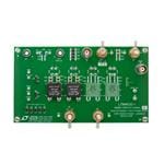
DC1437B-AA
Part Number : DC1437B-AA
Analog Devices Inc.RF Development Tools LTM9003-AA demo board, LVDS output, uses DC890 & LVDS_XFMR
HMC-C010
Part Number : HMC-C010
Analog Devices Inc.Sub-GHz Modules 600deg Anlg Phase Shift Module 6-15 GHz

HMC1019LP4E
Part Number : HMC1019LP4E
Analog Devices Inc.Attenuators 0.5 dB LSB 5-Bit dig atten , 0.1-30 GHz
HMC188MS8
Part Number : HMC188MS8
Analog Devices Inc.Signal Conditioning Passive Freq. Doubler, 1.25 - 3.0 GHz

RAPID-NI-V2109
Part Number : RAPID-NI-V2109
Analog Devices Inc.Networking Modules EtherNet/IP Netwrk module w/DLR Parallel
71M6543GT-IGTR/F
Part Number : 71M6543GT-IGTR/F
Analog Devices Inc.Metering Systems on a Chip - SoC 3-PHSE, 128KB, PRES TEMP SENSOR T/R

HMC855LC5
Part Number : HMC855LC5
Analog Devices Inc.Encoders, Decoders, Multiplexers & Demultiplexers 1:4 Demux
DC2164A-A
Part Number : DC2164A-A
Analog Devices Inc.Power Management IC Development Tools LTM4630EY-1 Demo Board - 70A, Two Step-D

AD7172-2BRUZ
Part Number : AD7172-2BRUZ
Analog Devices Inc.TThe AD7172-2 is an intelligent, low noise, low power, multiplexed,Σ-Δ analog-to-digital converter (ADC) with 2- or 4-channel(fully differential/single-ended) inputs for low bandwidthsignals. The AD7172-2 has a maximum channel scan rate of6.21 kSPS (161 µs) for fully settled data. The output data ratesrange from 1.25 SPS to 31.25 kSPS.The AD7172-2 integrates key analog and digital signal conditioningblocks to allow users to configure an individual setup for eachanalog input channel in use via the SPI. Integrated true rail-to-railbuffers on the analog inputs and external reference inputs provideeasy to drive high impedance inputs. The precision 2.5 V low drift(2 ppm/°C) band gap internal reference (with an output referencebuffer) adds embedded functionality to reduce the externalcomponent count.The digital filter allows simultaneous 50 Hz and 60 Hz rejectionat a 27.27 SPS output data rate. The user can switch betweendifferent filter options according to the demands of each channel inthe application, with further digital processing functions such asoffset and gain calibration registers, which are also configurable ona per channel basis. General-purpose inputs/outputs (GPIOs)control external multiplexers synchronous to the ADC conversiontiming.The specified operating temperature range is −40°C to +105°C.The AD7172-2 is in a 24-lead TSSOP package.Applications Process control: PLC/DCS modules - Temperature and pressure measurement Medical and scientific multichannel instrumentation Chromatography

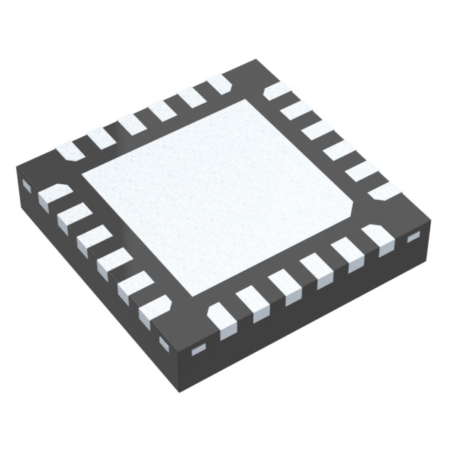
AD8285WBCPZ
Part Number : AD8285WBCPZ
Analog Devices Inc.The AD8285 is designed for low cost, low power, compact size, flexibility, and ease of use. It contains four channels of a low noise preamplifier (LNA) with a programmable gain amplifier (PGA) and an antialiasing filter (AAF) plus one direct-to-ADC channel, all integrated with a single 12-bit analog-to-digital converter (ADC).Each channel features a gain range of 16 dB to 34 dB in 6 dB increments and an ADC with a conversion rate of up to 72 MSPS. The combined input referred noise voltage of the entire channel is 3.5 nV/√Hz at maximum gain. The channel is optimized for dynamic performance and low power in applications where a small package size is critical.Fabricated in an advanced complementary metal oxide semiconductor (CMOS) process, the AD8285 is available in a 10 mm × 10 mm, RoHS compliant, 72-lead LFCSP that is specified over the automotive temperature range of −40°C to +105°C.APPLICATIONS Automotive radar Adaptive cruise control Collision avoidance Blind spot detection Self parking Electronic bumper

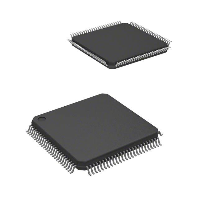
AD9208BBPZRL-3000
Part Number : AD9208BBPZRL-3000
Analog Devices Inc.The AD9208 is a dual, 14-bit, 3 GSPS analog-to-digital converter (ADC). The device has an on-chip buffer and a sample-and-hold circuit designed for low power, small size, and ease of use. This product is designed to support communications applications capable of direct sampling wide bandwidth analog signals of up to 5 GHz. The −3 dB bandwidth of the ADC input is 9 GHz. The AD9208 is optimized for wide input bandwidth, high sampling rate, excellent linearity, and low power in a small package.The dual ADC cores feature a multistage, differential pipelined architecture with integrated output error correction logic. Each ADC features wide bandwidth inputs supporting a variety of user-selectable input ranges. An integrated voltage referenceeases design considerations. The analog input and clock signals are differential inputs. The ADC data outputs are internally connected to four digital downconverters (DDCs) through a crossbar mux. Each DDC consists of up to five cascaded signalprocessing stages: a 48-bit frequency translator (numerically controlled oscillator (NCO)), and up to four half-band decimationfilters. The NCO has the option to select preset bands over the general-purpose input/output (GPIO) pins, which enables the selection of up to three bands. Operation of the AD9208 between the DDC modes is selectable via SPI-programmable profiles.In addition to the DDC blocks, the AD9208 has several functions that simplify the automatic gain control (AGC) function in acommunications receiver. The programmable threshold detector allows monitoring of the incoming signal power using the fast detect control bits in Register 0x0245 of the ADC. If the input signal level exceeds the programmable threshold, the fast detect indicator goes high. Because this threshold indicator has low latency, the user can quickly turn down the system gain to avoidan overrange condition at the ADC input. In addition to the fast detect outputs, the AD9208 also offers signal monitoring capability. The signal monitoring block provides additional information about the signal being digitized by the ADC.The user can configure the Subclasss 1 JESD204B-based high speed serialized output in a variety of one-lane, two-lane, four-lane, and eight-lane configurations, depending on the DDC configuration and the acceptable lane rate of the receiving logic device. Multidevice synchronization is supported through the SYSREF± and SYNCINB± input pins.The AD9208 has flexible power-down options that allow significant power savings when desired. All of these features canbe programmed using a 3-wire serial port interface (SPI).The AD9208 is available in a Pb-free, 196-ball BGA, specified over the −40°C to +85°C ambient temperature range. Thisproduct is protected by a U.S. patent.Note that throughout this data sheet, multifunction pins, such as FD_A/GPIO_A0, are referred to either by the entire pin name or by a single function of the pin, for example, FD_A, when only that function is relevant.Product Highlights Wide, input −3 dB bandwidth of 9 GHz supports direct radio frequency (RF) sampling of signals up to about 5 GHz. Four integrated, wideband decimation filter and NCO blocks supporting multiband receivers. Fast NCO switching enabled through GPIO pins. A SPI controls various product features and functions to meet specific system requirements. Programmable fast overrange detection and signal monitoring. On-chip temperature dioide for system thermal management. 12mm × 12mm 196-Lead BGAApplications Diversity multiband, multimode digital receivers 3G/4G, TD-SCDMA, W-CDMA, GSM, LTE, LTE-A Electronic test and measurement systems Phased array radar and electronic warfare DOCSIS 3.0 CMTS upstream receive paths HFC digital reverse path receivers

AD9363ABCZ
Part Number : AD9363ABCZ
Analog Devices Inc.The AD9363 is a high performance, highly integrated RF agiletransceiver designed for use in 3G and 4G femtocell applications.Its programmability and wideband capability make it ideal for abroad range of transceiver applications. The device combines anRF front end with a flexible mixed-signal baseband section andintegrated frequency synthesizers, simplifying design-in byproviding a configurable digital interface to a processor. TheAD9363 operates in the 325 MHz to 3.8 GHz range, coveringmost licensed and unlicensed bands. Channel bandwidths fromless than 200 kHz to 20 MHz are supported.The two independent direct conversion receivers have state-of-the-artnoise figure and linearity. Each Rx subsystem includesindependent automatic gain control (AGC), dc offset correction,quadrature correction, and digital filtering, thereby eliminatingthe need for these functions in the digital baseband. The AD9363also has flexible manual gain modes that can be externallycontrolled. Two high dynamic range ADCs per channel digitizethe received I and Q signals and pass them through configurabledecimation filters and 128-tap finite impulse response (FIR)filters to produce a 12-bit output signal at the appropriatesample rate.The transmitters use a direct conversion architecture that achieveshigh modulation accuracy with ultralow noise. This transmitterdesign produces a best-in-class Tx EVM of −34 dB, allowingsignificant system margin for the external power amplifier (PA)selection. The on-board Tx power monitor can be used as apower detector, enabling highly accurate Tx powermeasurements.The fully integrated phase-locked loops (PLLs) provide lowpower fractional N frequency synthesis for all receive andtransmit channels. Channel isolation, demanded by FDDsystems, is integrated into the design. All voltage controlledoscillators (VCOs) and loop filter components are integrated.The core of the AD9363 can be powered directly from a 1.3 Vregulator. The IC is controlled via a standard 4-wire serial portand four real-time I/O control pins. Comprehensive power-downmodes are included to minimize power consumption duringnormal use. The AD9363 is packaged in a 10 mm × 10 mm,144-ball chip scale package ball grid array (CSP_BGA).Applications 3G enterprise femtocell base stations 4G femtocell base stations Wireless video transmission


