AD532SD
Part Number : AD532SD
Analog Devices Inc.The AD532 is the first pretrimmed single chip monolithic multiplier/divider. It guarantees a maximum multiplying error of ±1.0% and a ±10 V output voltage without the need for any external trimming resistors or output op amp. Because the AD532 is internally trimmed, its simplicity of use provides design engineers with an attractive alternative to modular multipliers, and its monolithic construction provides significant advantages in size, reliability and economy. Further, the AD532 can be used as a direct replacement for other IC multipliers that require external trim networks (such as the AD530).APPLICATIONS Multiplication, division, squaring, square rooting Algebraic computation Power measurements Instrumentation applications Available in chip form
AD534SD
Part Number : AD534SD
Analog Devices Inc.The AD534 is a monolithic laser trimmed four-quadrant multiplier divider having accuracy specifications previously found only in expensive hybrid or modular products. A maximum multiplication error of ±0.25% is guaranteed for the AD534L without any external trimming. Excellent supply rejection, low temperature coefficients and long-term stability of the on-chip thin film resistors and buried Zener reference preserve accuracy even under adverse conditions of use. It is the first multiplier to offer fully differential, high impedance operation on all inputs, including the Z input, a feature that greatly increases its flexibility and ease of use. The scale factor is pretrimmed to the standard value of 10.00 V; by means of an external resistor, this can be reduced to values as low as 3 V.The wide spectrum of applications and the availability of several grades commend this multiplier as the first choice for all new designs. The AD534J (±1% maximum error), AD534K (±0.5% maximum), and AD534L (±0.25% maximum) are specified for operation over the 0°C to +70°C temperature range. The AD534S (±1% maximum) and AD534T (±0.5% maximum) are specified over the extended temperature range, −55°C to +125°C. All grades are available in hermetically sealed TO-100 metal cans and SBDIP packages. AD534K, AD534S, and AD534T chips are also available.APPLICATIONSHigh quality analog signal processingDifferential ratio and percentage computationsAlgebraic and trigonometric function synthesisWideband, high crest rms-to-dc conversionAccurate voltage controlled oscillators and filtersAvailable in chip form
AD5541LRZ
Part Number : AD5541LRZ
Analog Devices Inc.The AD5541 / AD5542 are single, 16-bit, serial input, voltage output digital-to-analog converters (DACs) that operate from a single 2.7 V to 5.5 V supply. The DAC output range extends from 0 V to VREF.The DAC output range extends from 0 V to VREF and is guaranteed monotonic, providing 1 LSB INL accuracy at 16 bits without adjustment over the full specified temperature range of −40°C to +85°C. Offering unbuffered outputs, the AD5541 / AD5542 achieve a 1 μs settling time with low power consumption and low offset errors. Providing a low noise performance of 11.8 nV/√Hz and low glitch, the AD5541 / AD5542 is suitable for deployment across multiple end systems.The AD5542 can be operated in bipolar mode, which generates a ±VREF output swing. The AD5542 also includes Kelvin sense connections for the reference and analog ground pins to reduce layout sensitivity.The AD5541 / AD5542 utilize a versatile 3-wire interface that is compatible with SPI, QSPI™, MICROWIRE™, and DSP interface standards. The AD5541 / AD5542 are available in 8-lead and 14-lead SOIC packages.PRODUCT HIGHLIGHTS Single-Supply Operation. The AD5541 and AD5542 are fully specified and guaranteed for a single 2.7 V to 5.5 V supply. Low Power Consumption. These parts consume typically 0.625 mW with a 5 V supply and 0.375 mW at 3 V. 3-Wire Serial Interface. Unbuffered Output Capable of Driving 60 kΩ Loads. This reduces power consumption because there is no internal buffer to drive. Power-On Reset Circuitry.APPLICATIONS Digital gain and offset adjustment Automatic test equipment Data acquisition systems Industrial process control
AD676JDZ
Part Number : AD676JDZ
Analog Devices Inc.The AD676 is a multipurpose 16-bit parallel output analog-to-digital converter which utilizes a switched-capacitor/charge redistribution architecture to achieve a 100 kSPS conversion rate (10 µs total conversion time). Overall performance is optimized by digitally correcting internal nonlinearities through on-chip autocalibration.The AD676 circuitry is segmented onto two monolithic chips- a digital control chip fabricated on Analog Devices DSP CMOS process and an analog ADC chip fabricated on our BiMOS II process. Both chips are contained in a single package.The AD676 is specified for ac (or 'dynamic') parameters such as S/(N+D) Ratio, THD and IMD which are important in signal processing applications. In addition, dc parameters are specified which are important in measurement applications.The AD676 operates from +5 V and ±12 V supplies and typically consumes 360 mW during conversion. The digital supply (VDD ) is separated from the analog supplies (VCC , VEE ) for reduced digital crosstalk. An analog ground sense is provided for the analog input. Separate analog and digital grounds are also provided.The AD676 is available in a 28-pin plastic DIP or 28-pin side-brazed ceramic package. A serial-output version, the AD677, is available in a 16-pin 300 mil wide ceramic or plastic package.
AD693AD
Part Number : AD693AD
Analog Devices Inc.The AD693 is a monolithic signal conditioning circuit which accepts low-level inputs from a variety of transducers to control a standard 4-20 mA, two-wire current loop. An on-chip voltage reference and auxiliary amplifier are provided for transducer excitation; up to 3.5 mA of excitation current is available when the device is operated in the loop-powered mode. Alternatively, the device may be locally powered for three-wire applications when 0-20 mA operation is desired.Precalibrated 30 mV and 60 mV input spans may be set by simple pin strapping. Other spans from 1 mV to 100 mV may be realized with the addition of external resistors. The auxiliary amplifier may be used in combination with on-chip voltages to provide six precalibrated ranges for 100 (ohm) RTDs. Output span and zero are also determined by pin strapping to obtain the standard ranges: 4-20mA, 12 ± 8 mA and 0-20 mA.Active laser trimming of the AD693's thin-film resistors result in high levels of accuracy without the need for additional adjustments and calibration. Total unadjusted error is tested on every device to be less than 0.5% of full scale at +25°C, and less than 0.75% over the industrial temperature range. Residual nonlinearity is under 0.05%. The AD693 also allows for the use of an external pass transistor to further reduce errors caused by self-heating.For transmission of low-level signals from RTDs, bridges and pressure transducers, the AD693 offers a cost-effective signal conditioning solution. It is recommended as a replacement for discrete designs in a variety of applications in process control, factory automation and system monitoring.The AD693 is packaged in a 20-pin ceramic side-brazed DIP, 20-pin Cerdip, and 20-pin LCCC and is specified over the -40°C to +85°C industrial temperature range.
AD7545CQ
Part Number : AD7545CQ
Analog Devices Inc.The AD7545 is a monolithic 12-bit CMOS multiplying DAC with onboard datalatches. It is loaded by a single 12-bit wide word and directly interfaces to most 12- and 16-bit bus systems. Data is loaded into the input latches under the control of the CS and WR inputs; tying these control inputs low makes the input latches transparent, allowing direct unbuffered operation of the DAC.The AD7545 is particularly suitable for single supply operationand applications with wide temperature variations.The AD7545 can be used with any supply voltage from +5 V to+15 V. With CMOS logic levels at the inputs the device dissipates less than 0.5 mW for VDD = +5 V.
OP162GSZ-REEL7
Part Number : OP162GSZ-REEL7
Analog Devices Inc.The OP162 (single), OP262 (dual), and OP462 (quad) rail-to-rail 15 MHz amplifiers feature the extra speed new designs require, with the benefits of precision and low power operation. With their incredibly low offset voltage of 45 µV (typical) and low noise, they are perfectly suited for precision filter applications and instrumentation. The low supply current of 500 µA (typical) is critical for portable or densely packed designs. In addition, the rail-to-rail output swing provides greater dynamic range and control than standard video amplifiers.These products operate from single supplies as low as 2.7 V to dual supplies of ±6 V. The fast settling times and wide output swings recommend them for buffers to sampling A/D converters. The output drive of 30 mA (sink and source) is needed for many audio and display applications; more output current can be supplied for limited durations. The OPx62 family is specified over the extended industrial temperature range (–40°C to +125°C). The single OP162 amplifiers are available in 8-lead SOIC package. The dual OP262 amplifiers are available in 8 lead SOIC and TSSOP packages. The quad OP462 amplifiers are available in 14-lead, narrow-body SOIC and TSSOP packages.
AD5254BRUZ100
Part Number : AD5254BRUZ100
Analog Devices Inc.The AD5253 / AD5254 are quad-channel, I2C, nonvolatile memory, digitally controlled potentiometers with 64/256 positions, respectively. These devices perform the same electronic adjustment functions as mechanical potentiometers, trimmers, and variable resistors.The parts’ versatile programmability allows multiple modes of operation, including read/write access in the RDAC and EEMEM registers, increment/decrement of resistance, resistance changes in ±6 dB scales, wiper setting readback, and extra EEMEM for storing user-defined information, such as memory data for other components, look-up table, or system identification information.The AD5253 / AD5254 allow the host I2C controllers to write any of the 64-/256-step wiper settings in the RDAC registers and store them in the EEMEM. Once the settings are stored, they are restored automatically to the RDAC registers at system power-on; the settings can also be restored dynamically.The AD5253 / AD5254 provide additional increment, decrement, +6 dB step change, and –6 dB step change in synchronous or asynchronous channel update mode. The increment and decrement functions allow stepwise linear adjustments, with a ± 6 dB step change equivalent to doubling or halving the RDAC wiper setting. These functions are useful for steep-slope, nonlinear adjustments, such as white LED brightness and audio volume control.The AD5253 / AD5254 have a patented resistance-tolerance storing function that allows the user to access the EEMEM and obtain the absolute end-to-end resistance values of the RDACs for precision applications.The AD5253 / AD5254 are available in TSSOP-20 packages in 1 kΩ, 10 kΩ, 50 kΩ, and 100 kΩ options. All parts are guaranteed to operate over the –40°C to +105°C extended industrial temperature range. In this data sheet, the nonvolatile memory and EEMEM terms are used interchangeably, as are the digital potentiometer and RDAC terms.APPLICATIONS Mechanical potentiometer replacement Low resolution DAC replacement RGB LED backlight control White LED brightness adjustment RF base station power amp bias control Programmable gain and offset control Programmable attenuators Programmable voltage-to-current conversion Programmable power supply Programmable filters Sensor calibrations
AD5290YRMZ100
Part Number : AD5290YRMZ100
Analog Devices Inc.The AD5290 is one of the few high voltage, high performance, and compact digital potentiometers1 in the market at present. This device can be used as a programmable resistor or resistor divider. The AD5290 performs the same electronic adjustment function as mechanical potentiometers, variable resistors, and trimmers, with enhanced resolution, solid-state reliability, and superior temperature stability.With digital rather than manual control, the AD5290 provides layout flexibility and allows closed-loop dynamic controllability.The AD5290 is available in MSOP-10 package and has 10 kΩ, 50 kΩ, and 100 kΩ options. All parts are guaranteed to operate over the –40°C to +125°C extended automotive temperature range.Applications High voltage DAC Programmable power supply Programmable gain and offset adjustment Programmable filters and delays Actuator control Audio volume control Mechanical potentiometer replacement1 The RDAC segmentation is protected by U.S. Patent Number 5,495,245.
AD5305ARMZ
Part Number : AD5305ARMZ
Analog Devices Inc.The AD5305 / AD5315 / AD5325 are quad 8-, 10-, and 12-bit buffered voltage output DACs in a 10-lead MSOP that operate from a single 2.5 V to 5.5 V supply, consuming 500 μA at 3 V. Their on-chip output amplifiers allow rail-to-rail output swing with a slew rate of 0.7 V/μs. A 2-wire serial interface that operates at clock rates up to 400 kHz is used. This interface is SMBus compatible at VDD < 3.6 V. Multiple devices can be placed on the same bus.The references for the four DACs are derived from one reference pin. The outputs of all DACs can be updated simultaneously using the software LDAC function.The parts incorporate a power-on reset circuit, which ensures that the DAC outputs power up to 0 V and remain there until a valid write takes place to the device. There is also a software clear function to reset all input and DAC registers to 0 V. The parts contain a power-down feature that reduces the current consumption of the devices to 200 nA @ 5 V (80 nA @ 3 V).The low power consumption of these parts in normal operation makes them ideally suited for portable battery-operated equipment. The power consumption is 3 mW at 5 V, 1.5 mW at 3 V, reducing to 1 μW in power-down mode.APPLICATIONS Portable battery-powered instruments Digital gain and offset adjustment Programmable voltage and current sources Programmable attenuators Industrial process control
AD5312ARMZ
Part Number : AD5312ARMZ
Analog Devices Inc.The AD5302/AD5312/AD5322 are dual 8-, 10- and 12-bit buffered voltage output DACs in a 10-lead µSOIC package that operate from a single +2.5 V to +5.5 V supply consuming 230 µA at 3 V. Their on-chip output amplifiers allow the outputs to swing rail-to-rail with a slew rate of 0.7 V/µs. The AD5302/ AD5312/AD5322 utilize a versatile 3-wire serial interface which operates at clock rates up to 30 MHz and is compatible with standard SPI™, QSPI™, MICROWIRE™ and DSP interface standards.PRODUCT HIGHLIGHTS Available in 10-lead MicroSOIC packages Low power, single supply operation from 2.5 V to 5.5 V supply Consumes 0.7mW at 3 V and 1.5 mW at 5 V Rail-to-Rail output with a slew rate of 0.7 V/µs Utilizes a versatile 3-wire serial interface with clock rates up to 30 MHz Pin and Software Compatible with the AD5302 (8-Bit) and the AD5322 (12-bit)
AD5324BRMZ
Part Number : AD5324BRMZ
Analog Devices Inc.The AD5304/AD5314/AD5324 are quad 8-, 10-, and 12-bit buffered voltage output DACs in 10-lead MSOP and 10-lead LFCSP packages that operate from a single 2.5 V to 5.5 V supply, consuming 500 μA at 3 V. Their on-chip output amplifiers allow rail-to-rail output swing to be achieved with a slew rate of 0.7 V/μs. A 3-wire serial interface is used; it operates at clock rates up to 30 MHz and is compatible with standard SPI, QSPI, MICROWIRE, and DSP interface standards.The references for the four DACs are derived from one reference pin. The outputs of all DACs can be updated simultaneously using the software LDAC function. The parts incorporate a power-on reset circuit, and ensure that the DAC outputs power up to 0 V and remains there until a valid write takes place to the device. The parts contain a power-down feature that reduces the current consumption of the device to 200 nA @ 5 V (80 nA @ 3 V).The low power consumption of these parts in normal operation makes them ideally suited to portable battery-operated equipment. The power consumption is 3 mW at 5 V, 1.5 mW at 3 V, reducing to 1 μW in power-down mode.Applications Portable battery-powered instruments Digital gain and offset adjustment Programmable voltage and current sources Programmable attenuators Industrial process controls
AD5391BSTZ-3
Part Number : AD5391BSTZ-3
Analog Devices Inc.The AD5390 / AD5391 are complete single-supply, 16-channel, 14-bit and 12-bit DACs, respectively. The AD5392 is a complete single-supply, 8-channel, 14-bit DAC. The devices are available in either a 64-lead LFCSP or a 52-lead LQFP. All channels have an on-chip output amplifier with rail-to-rail operation. All devices include an internal 1.25/2.5 V, 10 ppm/°C reference, an on-chip channel monitor function that multiplexes the analog outputs to a common MON_OUT pin for external monitoring, and an output amplifier boost mode that optimizes the output amplifier slew rate.The AD5390 / AD5391 / AD5392 contain a 3-wire serial interface with interface speeds in excess of 30 MHz that are compatible with SPI®, QSPI™, MICROWIRE™, and DSP interface standards and an I2C-compatible interface supporting a 400 kHz data transfer rate.An input register followed by a DAC register provides double-buffering, allowing DAC outputs to be updated independently or simultaneously using the LDAC input. Each channel has a programmable gain and offset adjust register, letting the user fully calibrate any DAC channel.Power consumption is typically 0.25 mA per channel.APPLICATIONS Instrumentation and industrial control Power amplifier control Level setting (ATE) Control systems Microelectromechanical systems (MEMS) Variable optical attenuators (VOAs) Optical transceivers (MSA 300, XFP)
AD5624RBRMZ-5
Part Number : AD5624RBRMZ-5
Analog Devices Inc.The AD5624R/AD5644R/AD5664R, members of the nanoDAC® family, are low power, quad, 12-/14-/16-bit buffered voltage-out DACs. All devices operate from a single 2.7 V to 5.5 V supply and are guaranteed monotonic by design.The AD5624R/AD5644R/AD5664R have an on-chip reference. The AD56x4R-3 has a 1.25 V, 5 ppm/°C reference, giving a full-scale output range of 2.5 V; the AD56x4R-5 has a 2.5 V, 5 ppm/°C reference giving a full-scale output range of 5 V. The on-chip reference is off at power-up, allowing the use of an external reference; all devices can be operated from a single 2.7 V to 5.5 V supply. The internal reference is enabled via a software write.The part incorporates a power-on reset circuit that ensures the DAC output powers up to 0 V and remains there until a valid write takes place. The part contains a per-channel power-down feature that reduces the current consumption of the device to 480 nA at 5 V and provides software-selectable output loads while in power-down mode. The low power consumption of this part in normal operation makes it ideally suited to portable battery-operated equipment.The AD5624R/AD5644R/AD5664R use a versatile 3-wire serial interface that operates at clock rates up to 50 MHz, and is compatible with standard SPI, QSPI™, MICROWIRE™, and DSP interface standards. The on-chip precision output amplifier enables rail-to-rail output swing.Product Highlights Quad 12-/14-/16-bit DACs. On-chip 1.25 V/2.5 V, 5 ppm/°C reference. Available in 10-lead MSOP; 10-lead, 3 mm × 3 mm LFCSP_WD; and 12-ball, 1.665 mm × 2.245 mm WLCSP. Low power, typically consumes 1.32 mW at 3 V and 2.25 mW at 5 V.Applications Process controls Data acquisition systems Portable battery-powered instruments Digital gain and offset adjustment Programmable voltage and current sources Programmable attenuators
AD588AQ
Part Number : AD588AQ
Analog Devices Inc.The AD588 represents a major advance in state-of-the-art monolithic voltage references. Low initial error and low temperature drift give the AD588 absolute accuracy performance previously not available in monolithic form. The AD588 uses a proprietary ion-implanted, buried Zener diode and laser-wafer drift trimming of high stability thin film resistors to provide outstanding performance.The AD588 includes the basic reference cell and three additional amplifiers that provide pin programmable output ranges. The amplifiers are laser trimmed for low offset and low drift to maintain the accuracy of the reference. The amplifiers are configured to allow Kelvin connections to the load and/or boosters for driving long lines or high current loads, delivering the full accuracy of the AD588 where it is required in the application circuit.The low initial error allows the AD588 to be used as a system reference in precision measurement applications requiring 12-bit absolute accuracy. In such systems, the AD588 can provide a known voltage for system calibration in software. The low drift also allows compensation for the drift of other components in a system. Manual system calibration and the cost of periodic recalibration can, therefore, be eliminated. Furthermore, the mechanical instability of a trimming potentiometer and the potential for improper calibration can be eliminated by using the AD588 in conjunction with auto calibration software.The AD588 is available in seven versions. The AD588JQ and AD588KQ are packaged in a 16-lead CERDIP and are specified for 0°C to +70°C operation. The AD588AQ and AD588BQ are packaged in a 16-lead CERDIP, and the AD588ARWZ is packaged in a 16-lead SOIC, and they are specified for the −25°C to +85°C industrial temperature range. The ceramic AD588TE and AD588TQ grades are specified for the full military/aerospace temperature range.Product HighlightsThe AD588 offers 12-bit absolute accuracy without any user adjustments. Optional fine-trim connections are provided for applications requiring higher precision. The fine trimming does not alter the operating conditions of the Zener or the buffer amplifiers, and so does not increase the temperature drift.Output noise of the AD588 is very low, typically 6 μV p-p. A pin is provided for additional noise filtering using an external capacitor.A precision ±5 V tracking mode with Kelvin output connections is available with no external components. Tracking error is less than 1 mV, and a fine trim is available for applications requiring exact symmetry between the +5 V and −5 V outputs.Pin strapping capability allows configuration of a wide variety of outputs: ±5 V, +5 V, +10 V, −5 V, and −10 V dual outputs or +5 V, −5 V, +10 V, and −10 V single outputs.
AD600JRZ
Part Number : AD600JRZ
Analog Devices Inc.The AD600/AD602 dual channel, low noise, variable gain amplifiers are optimized for use in ultrasound imaging systems, but are applicable to any application requiring precise gain, low noise and distortion, and wide bandwidth. Each independent channel provides a gain of 0 dB to +40 dB in the AD600 and -10 dB to +30 dB in the AD602. The lower gain of the AD602 results in an improved signal-to-noise ratio (SNR) at the output. However, both products have the same 1.4 nV/√Hz input noise spectral density. The decibel gain is directly proportional to the control voltage, accurately calibrated, and supply and temperature-stable.To achieve the difficult performance objectives, a proprietary circuit form, the X-AMP®, was developed. Each channel of the X-AMP comprises a variable attenuator of 0 dB to -42.14 dB followed by a high speed fixed gain amplifier. In this way, the amplifier never has to cope with large inputs, and can benefit from the use of negative feedback to precisely define the gain and dynamics. The attenuator is realized as a 7-stage R-2R ladder network having an input resistance of 100 W, laser trimmed to ±2%. The attenuation between tap points is 6.02 dB; the gain-control circuit provides continuous interpolation between these taps. The resulting control function is linear in dB.The gain-control interfaces are fully differential, providing an input resistance of ~15 M W and a scale factor of 32 dB/V (that is, 31.25 mV/dB) defined by an internal voltage reference. The response time of this interface is less than 1 µs. Each channel also has an independent gating facility that optionally blocks signal transmission and sets the dc output level to within a few millivolts of the output ground. The gating control input is TTL- and CMOS-compatible.The maximum gain of the AD600 is 41.07 dB, and the maximum gain of the AD602 is 31.07 dB; the -3 dB bandwidth of both models is nominally 35 MHz, essentially independent of the gain. The SNR for a 1 V rms output and a 1 MHz noise bandwidth is typically 76 dB for the AD600 and 86 dB for the AD602. The amplitude response is flat within ±0.5 dB from 100 kHz to 10 MHz; over this frequency range, the group delay varies by less than ±2 ns at all gain settings.Each amplifier channel can drive 100 W load impedances with low distortion. For example, the peak specified output is ±2.5 V minimum into a 500 W load, or ±1 V into a 100 W load. For a 200 W load in shunt with 5 pF, the total harmonic distortion for a ±1 V sinusoidal output at 10 MHz is typically -60 dBc.The AD600J/AD602J are specified for operation from 0°C to 70°C and are available in 16-lead PDIP (N) and 16-lead SOIC packages. The AD600A/AD602A are specified for operation from -40°C to +85°C and are available in 16-lead CERDIP (Q) and 16-lead SOIC packages. The AD600S/AD602S are specified for operation from -55°C to +125°C, are available in a 16-lead CERDIP (Q) package, and are MIL-STD-883 compliant. The AD600S/AD602S are also available under DESC SMD 5962-94572.AD600 - Gain Range: 0 dB to 40 dBAD602 - Gain Range: -10 dB to + 30 dB
AD71056ARZ
Part Number : AD71056ARZ
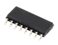
Analog Devices Inc.The ADE7757A (AD71056) is an accurate electrical energy measurement integrated circuit. It is a pin reduction version of ADE7755 with an enhancement of a precise oscillator circuit that serves as a clock source to the chip. The ADE7757A eliminates the cost of an external crystal or resonator, thus reducing the overall cost of a meter built with this IC. The chip directly interfaces with shunt resistor.The ADE7757A provides instantaneous and average real power based on line current and voltage. The part specifications surpass the accuracy requirements as quoted in the IEC61036 standard. The only analog circuitry used in the ADE7757A is in the ADCs and reference circuit. All other signal processing (e.g., multiplication and filtering) is carried out in the digital domain. This approach provides superior stability and accuracy over extremes in environmental conditions and over time.The small analog input full-scale allows the chip to interface to low value shunt resistances without losing dynamic range. The ADE7757A is available in 16-lead SOIC narrow-body package.The Application Note AN-679 can be used as a basis for a description of an IEC62053-21 low cost, watt-hour meter reference design.NOTE: For polyphase system designs, the ADE7752A is recommended.
AD725ARZ
Part Number : AD725ARZ
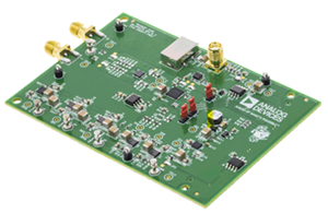
Analog Devices Inc.The AD725 is a very low cost general purpose RGB to NTSC/PAL encoder that converts red, green and blue color componentsignals into their corresponding luminance (basebandamplitude) and chrominance (subcarrier amplitude and phase)signals in accordance with either NTSC or PAL standards.These two outputs are also combined on-chip to provide acomposite video output. All three outputs are available separatelyat voltages of twice the standard signal levels as requiredfor driving 75 Ω, reverse-terminated cables.An evaluation board is available for this product and may be ordered using the following product number: AD725-EB.
AD7324BRUZ
Part Number : AD7324BRUZ
Analog Devices Inc.The AD7324 is a 4-channel, 12-bit plus sign, successive approximation ADC designed on the iCMOS (industrial CMOS) process. iCMOS is a process combining high voltage silicon with submicron CMOS and complementary bipolar technologies. It enables the development of a wide range of high performance analog ICs capable of 33 V operation in a footprint that no previous generation of high voltage parts could achieve. Unlike analog ICs using conventional CMOS processes, iCMOS components can accept bipolar input signals while providing increased performance, dramatically reduced power consumption, and reduced package size.The AD7324 can accept true bipolar analog input signals. The AD7324 has four software-selectable input ranges: ±10 V, ±5 V, ±2.5 V, and 0 V to +10 V. Each analog input channel can be independently programmed to one of the four input ranges. The analog input channels on the AD7324 can be programmed to be single-ended, true differential, or pseudo differential.The ADC contains a 2.5 V internal reference. The AD7324 also allows for external reference operation. If a 3 V reference is applied to the REFIN/OUT pin, the AD7324 can accept a true bipolar ±12 V analog input. Minimum ±12 V VDD and VSS supplies are required for the ±12 V input range. The ADC has a high speed serial interface that can operate at throughput rates up to 1 MSPS.PRODUCT HIGHLIGHTS The AD7324 can accept true bipolar analog input signals, ±10 V, ±5 V, ±2.5 V, and 0 V to +10 V unipolar signals. The four analog inputs can be configured as four single-ended inputs, two true differential input pairs, two pseudo differential inputs, or three pseudo differential inputs. 1 MSPS serial interface. SPI®-/QSPI™-/DSP-/MICROWIRE™-compatible interface. Low power, 31 mW maximum, at 1 MSPS throughput rate. Channel sequencer.
AD7327BRUZ-REEL
Part Number : AD7327BRUZ-REEL
Analog Devices Inc.The AD73271 is an 8-Channel, 12-Bit plus Sign Successive Approximation ADC designed on the iCMOS (industrial CMOS) process. iCMOS is a process combining high voltage silicon with submicron CMOS and complementary bipolar technologies. It enables the development of a wide range of high performance analog ICs capable of 33 V operation in a footprint that no previous generation of high voltage parts could achieve. Unlike analog ICs using conventional CMOS processes, iCMOS components can accept bipolar input signals while providing increased performance, dramatically reduced power consumption, and reduced package size.The AD7327 can accept true bipolar Analog Input signals. The AD7327 has four software selectable inputs Ranges, ±10 V, ±5 V, ±2.5 V and 0 to 10 V. Each analog input channel can be independently programmed to one of the four input ranges. The Analog input channels on the AD7327 can be programmed to be Single-Ended, true Differential or Pseudo Differential.The ADC contains a 2.5 V Internal reference. The AD7327 also allows for external Reference operation. If a 3 V reference is applied the REFIN/OUT pin the AD7327 can accept a true Bipolar ±12V Analog Input. VDD and VSS supplies of ±12V are required for the ±12 V Input Range. The ADC has a high speed serial interface that can operate at throughput rates up to 500 kSPS.Product Highlights The AD7327 can accept True Bipolar Analog Input signals, ±10 V, ±5 V, ±2.5 V and 0 to 10 V unipolar signals. The Eight Analog Inputs can be configured as 8 Single-Ended inputs, 4 True Differential, 4 Pseudo Differential or 7 Pseudo Differential Inputs. The ADC has a high speed serial interface that can operate at throughput rates up to 500 kSPS. Low power, 18 mW, at a maximum throughput rate of 500 kSPS. Channel Sequencer.


