ADR425BRZ
Part Number : ADR425BRZ
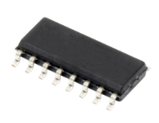
Analog Devices Inc.The ADR42x are a series of ultraprecision, second generation eXtra implanted junction FET (XFET) voltage references featuring low noise, high accuracy, and excellent long-term stability in SOIC and MSOP footprints.Patented temperature drift curvature correction technique and XFET technology minimize nonlinearity of the voltage change with temperature. The XFET architecture offers superior accuracy and thermal hysteresis to the band gap references. It also operates at lower power and lower supply headroom than the buried Zener references.The superb noise and the stable and accurate characteristics of the ADR42x make them ideal for precision conversion applications such as optical networks and medical equipment. The ADR42x trim terminal can also be used to adjust the out-put voltage over a ±0.5% range without compromising any other performance. The ADR42x series voltage references offer two electrical grades and are specified over the extended industrial temperature range of −40°C to +125°C. Devices have 8-lead SOIC or 30% smaller, 8-lead MSOP packages.APPLICATIONS Precision data acquisition systems High resolution converters Battery-powered instrumentation Portable medical instruments Industrial process control systems Precision instruments Optical network control circuits
ADR441ARMZ-REEL7
Part Number : ADR441ARMZ-REEL7
Analog Devices Inc.The ADR440/ADR441/ADR443/ADR444/ADR445 series is a family of XFET® voltage references featuring ultralow noise, high accuracy, and low temperature drift performance. Using Analog Devices, Inc., patented temperature drift curvature correction and XFET (eXtra implanted junction FET) technology, voltage change vs. temperature nonlinearity in the ADR440/ADR441/ADR443/ADR444/ADR445 is greatly minimized.The XFET references offer better noise performance than buried Zener references, and XFET references operate off low supply voltage headroom (500 mV). This combination of features makes the ADR440/ADR441/ADR443/ADR444/ADR445 family ideally suited for precision signal conversion applications in high-end data acquisition systems, optical networks, and medical applications.The ADR440/ADR441/ADR443/ADR444/ADR445 family has the capability to source up to 10 mA of output current and sink up to −5 mA. It also comes with a trim terminal to adjust the output voltage over a 0.5% range without compromising performance.The ADR440/ADR441/ADR443/ADR444/ADR445 family is available in 8-lead MSOP and narrow SOIC packages and offered in two electrical grades. All versions are specified over the extended industrial temperature range of −40°C to +125°C.Applications Precision data acquisition systems High resolution data converters Battery-powered instrumentation Portable medical instruments Industrial process control systems Precision instruments Optical control circuits
ADT7310TRZ
Part Number : ADT7310TRZ
Analog Devices Inc.The ADT7310 is a high accuracy digital temperature sensor in a narrow SOIC package. It contains a band gap temperature reference and a 13-bit ADC to monitor and digitize the temperature to a 0.0625°C resolution. The ADC resolution, by default, is set to 13 bits (0.0625 °C). This can be changed to 16 bits (0.0078 °C) by setting Bit 7 in the configuration register (Register Address 0x01).The ADT7310 is guaranteed to operate over supply voltages from 2.7 V to 5.5 V. Operating at 3.3 V, the average supply current is typically 210 μA. The ADT7310 has a shutdown mode that powers down the device and offers a shutdown current of typically 2 μA. The ADT7310 is rated for operation over the −55°C to +150°C temperature range.The CT pin is an open-drain output that becomes active when the temperature exceeds a programmable critical temperature limit. The default critical temperature limit is 147°C. The INT pin is also an open-drain output that becomes active when the temperature exceeds a programmable limit. The INT and CT pins can operate in either comparator or interrupt mode.APPLICATIONS Medical equipment Environmental control systems Computer thermal monitoring Thermal protection Industrial process control Power system monitors Hand-held applications
ADT7410TRZ
Part Number : ADT7410TRZ
Analog Devices Inc.The ADT7410 is a high accuracy digital temperature sensor in anarrow SOIC package. It contains a band gap temperature referenceand a 13-bit ADC to monitor and digitize the temperature to a0.0625°C resolution. The ADC resolution, by default, is set to13 bits (0.0625°C). This can be changed to 16 bits (0.0078°C) bysetting Bit 7 in the configuration register (Register Address 0x03).The ADT7410 is guaranteed to operate over supply voltages from2.7 V to 5.5 V. Operating at 3.3 V, the average supply current is typically210 μA. The ADT7410 has a shutdown mode that powersdown the device and offers a shutdown current of typically 2 μA.The ADT7410 is rated for operation over the −55°C to +150°Ctemperature range.Pin A0 and Pin A1 are available for address selection, giving theADT7410 four possible I2C addresses. The CT pin is an open-drainoutput that becomes active when the temperature exceedsa programmable critical temperature limit. The default criticaltemperature limit is 147°C. The INT pin is also an open-drainoutput that becomes active when the temperature exceeds aprogrammable limit. The INT and CT pins can operate in eithercomparator or interrupt mode.Applications Medical equipment Environmental control systems Computer thermal monitoring Thermal protection Industrial process control Power system monitors Hand-held applications
ADUC7019BCPZ62I
Part Number : ADUC7019BCPZ62I
Analog Devices Inc.The ADuC7019 / ADuC7020 / ADuC7021 / ADuC7022 / ADuC7024 / ADuC7025 / ADuC7026 / ADuC7027 / ADuC7028 / ADuC7029 are fully integrated,1 MSPS, 12-bit data acquisition systems incorporating highperformance multichannel ADCs, 16-bit/32-bit MCUs, andFlash®/EE memory on a single chip.The ADC consists of up to 12 single-ended inputs. An additionalfour inputs are available but are multiplexed with the four DACoutput pins. The four DAC outputs are available only on certainmodels (ADuC7020, ADuC7026, ADuC7028, and ADuC7029).However, in many cases where the DAC outputs are not present,these pins can still be used as additional ADC inputs, giving amaximum of 16 ADC input channels. The ADC can operate insingle-ended or differential input mode. The ADC input voltageis 0 V to VREF. A low drift band gap reference, temperature sensor,and voltage comparator complete the ADC peripheral set.Depending on the part model, up to four buffered voltageoutput DACs are available on-chip. The DAC output range isprogrammable to one of three voltage ranges.The devices operate from an on-chip oscillator and a PLLgenerating an internal high frequency clock of 41.78 MHz(UCLK). This clock is routed through a programmable clockdivider from which the MCU core clock operating frequencyis generated. The microcontroller core is an ARM7TDMI®,16-bit/32-bit RISC machine, which offers up to 41 MIPS peakperformance. Eight kilobytes of SRAM and 62 kilobytes ofnonvolatile Flash/EE memory are provided on-chip. TheARM7TDMI core views all memory and registers as a singlelinear array.On-chip factory firmware supports in-circuit serial downloadvia the UART or I2C serial interface port; nonintrusive emulationis also supported via the JTAG interface. These features areincorporated into a low cost QuickStart™ development systemsupporting this MicroConverter® family.The parts operate from 2.7 V to 3.6 V and are specified over anindustrial temperature range of −40°C to +125°C. Whenoperating at 41.78 MHz, the power dissipation is typically120 mW. The ADuC7019 / ADuC7020 / ADuC7021 / ADuC7022 / ADuC7024 / ADuC7025 / ADuC7026 / ADuC7027 / ADuC7028 / ADuC7029 areavailable in a variety of memory models and packages (seeOrdering Guide).APPLICATIONS Industrial control and automation systems Smart sensors, precision instrumentation Base station systems, optical networking
ADUC7128BSTZ126
Part Number : ADUC7128BSTZ126
Analog Devices Inc.The ADuC7128 / ADuC7129 are fully integrated, 1 MSPS, 12-bit data acquisition systems incorporating a high performance, multi-channel analog-to-digital converter (ADC), DDS with line driver, 16-/32-bit MCU, and Flash/EE memory on a single chip.The ADC consists of up to 14 single-ended inputs. The ADC can operate in single-ended or differential input modes. The ADC input voltage is 0 to VREF. Low drift band gap reference, temperature sensor, and voltage comparator complete the ADC peripheral set.The ADuC7128/ADuC7129 integrate a differential line driver output. This line driver transmits a sine wave whose values are calculated by an on-chip DDS or a voltage output determined by the DACDAT MMR.The devices operate from an on-chip oscillator and PLL, generating an internal high frequency clock of 41.78 MHz. This clock is routed through a programmable clock divider from which the MCU core clock operating frequency is generated.The microcontroller core is an ARM7TDMI®, 16-/32-bit reduced instruction set computer (RISC), offering up to 41 MIPS peak performance. There are 126 kB of nonvolatile Flash/EE provided on-chip, as well as 8 kB of SRAM. The ARM7TDMI core views all memory and registers as a single linear array.On-chip factory firmware supports in-circuit serial download via the UART serial interface port, and nonintrusive emulation is also supported via the JTAG interface. These features are incorporated into a low cost QuickStart™ development system supporting this MicroConverter® family.The parts operate from 3.0 V to 3.6 V and are specified over an industrial temperature range of −40°C to +125°C. When operating at 41.78 MHz, the power dissipation is 135 mW. The line driver output, if enabled, consumes an additional 30 mW.
ADUM1100ARZ
Part Number : ADUM1100ARZ
Analog Devices Inc.The ADuM1100 is a digital isolator based on Analog Devices Inc., iCoupler® technology. Combining high speed CMOS and monolithic air core transformer technology, this isolation component provides outstanding performance characteristics superior to alternatives, such as optocoupler devices.Configured as a pin-compatible replacement for existing high speed optocouplers, the ADuM1100 supports data rates as high as 25 Mbps and 100 Mbps.The ADuM1100 operates with a voltage supply ranging from 3.0 V to 5.5 V, boasts a propagation delay of
ADUM1301BRWZ
Part Number : ADUM1301BRWZ
Analog Devices Inc.The ADuM130x are triple-channel digital isolators based on the Analog Devices, Inc., iCoupler® technology. Combining high speed CMOS and monolithic transformer technology, these isolation components provide outstanding performance characteristics superior to alternatives, such as optocouplers.By avoiding the use of LEDs and photodiodes, iCoupler devices remove the design difficulties commonly associated with optocouplers. The typical optocoupler concerns regarding uncertain current transfer ratios, nonlinear transfer functions, and temperature and lifetime effects are eliminated with the simple iCoupler digital interfaces and stable performance characteristics. The need for external drivers and other discrete components is eliminated with these iCoupler products. Furthermore, iCoupler devices consume one-tenth to one-sixth of the power of optocouplers at comparable signal data rates.The ADuM130x isolators provide three independent isolation channels in a variety of channel configurations and data rates (see the Ordering Guide in the data sheet). Both models operate with the supply voltage on either side ranging from 2.7 V to 5.5 V, providing compatibility with lower voltage systems as well as enabling a voltage translation functionality across the isolation barrier. In addition, the ADuM130x provide low pulse width distortion (
ADUM1301CRWZ
Part Number : ADUM1301CRWZ
Analog Devices Inc.The ADuM130x are triple-channel digital isolators based on the Analog Devices, Inc., iCoupler® technology. Combining high speed CMOS and monolithic transformer technology, these isolation components provide outstanding performance characteristics superior to alternatives, such as optocouplers.By avoiding the use of LEDs and photodiodes, iCoupler devices remove the design difficulties commonly associated with optocouplers. The typical optocoupler concerns regarding uncertain current transfer ratios, nonlinear transfer functions, and temperature and lifetime effects are eliminated with the simple iCoupler digital interfaces and stable performance characteristics. The need for external drivers and other discrete components is eliminated with these iCoupler products. Furthermore, iCoupler devices consume one-tenth to one-sixth of the power of optocouplers at comparable signal data rates.The ADuM130x isolators provide three independent isolation channels in a variety of channel configurations and data rates (see the Ordering Guide in the data sheet). Both models operate with the supply voltage on either side ranging from 2.7 V to 5.5 V, providing compatibility with lower voltage systems as well as enabling a voltage translation functionality across the isolation barrier. In addition, the ADuM130x provide low pulse width distortion (
AD843KNZ
Part Number : AD843KNZ
Analog Devices Inc.The AD843 is a fast settling, 34 MHz, CBFET input op amp. The AD843 combines the low (0.6 nA) input bias currents characteristic of a FET input amplifier while still providing a 34 MHz bandwidth and a 135 ns settling time (to within 0.01% of final value for a 10 volt step). The AD843 is a member of the Analog Devices' family of wide bandwidth operational amplifiers. These devices are fabricated using Analog Devices' junction isolated complementary bipolar (CB) process. This process permits a combination of dc precision and wideband ac performance previously unobtainable in a monolithic op amp.The 250 V/µs slew rate and 0.6 nA input bias current of the AD843 ensure excellent performance in high speed sample-and-hold applications and in high speed integrators. This amplifier is also ideally suited for high bandwidth active filters and high frequency signal conditioning circuits.Unlike many high frequency amplifiers, the AD843 requires no external compensation and it remains stable over its full operating temperature range. It is available in five performance grades: the AD843J and AD843K are rated over the commercial temperature range of 0°C to +70°C. The AD843A and AD843B are rated over the industrial temperature range of -40°C to +85°C. The AD843S is rated over the military temperature range of -55°C to +125°C and is available processed to MIL-STD-883B, Rev. C.
AD845BQ
Part Number : AD845BQ
Analog Devices Inc.The AD845 is a fast, precise, N channel JFET input, monolithic operational amplifier. It is fabricated using Analog Devices' complementary bipolar (CB) process. Advanced laser-wafer trimming technology enables the very low input offset voltage and offset voltage drift performance to be realized. This precision, when coupled with a slew rate of 100 V/µs, a stable unity-gain bandwidth of 16 MHz, and a settling time of 350 ns 0.01%-while driving a parallel load of 100 pF and 500 Ohm- represents a combination of features unmatched by any FET input IC amplifier. The AD845 can easily be used to upgrade many existing designs which use BiFET or FET input hybrid amplifiers and, in some cases, those which use bipolar input op amps.The AD845 is ideal for use in applications such as active filters, high speed integrators, photo diode preamps, sample-and-hold amplifiers, log amplifiers, and in buffering A/D and D/A converters. The 250 µV max input offset voltage makes offset nulling unnecessary in many applications. The common-mode rejection ratio of 110 dB over a ±10 V input voltage range represents exceptional performance for a JFET input high speed op amp. This, together with a minimum open-loop gain of 250 V/mV ensures that 12-bit performance is achieved, even in unity-gain buffer circuits.The AD845 conforms to the standard op amp pinout except that offset nulling is to V+. The AD845J and AD845K grade devices are available specified to operate over the commercial 0°C to +70°C temperature range. AD845A and AD845B devices are specified for operation over the -40°C to +85°C industrial temperature range. The AD845S is specified to operate over the full military temperature range of -55°C to +125°C. Both the industrial and military versions are available in 8-pin cerdip packages. The commercial version is available in an 8-pin plastic mini-DIP and 16-pin SOIC; 'J' and 'S' grade chips are also available.
AD8620BRZ
Part Number : AD8620BRZ
Analog Devices Inc.The AD8610 (single) and AD8620 (dual) are very high precision JFET input amplifiers featuring ultralow offset voltage and drift, very low input voltage and current noise, very low input bias current, and wide bandwidth. Unlike many JFET amplifiers, the AD8610 input bias current is low over the entire operating temperature range. The AD8610 is stable with capacitive loads of over 1000 pF in noninverting unity gain; much larger capacitive loads can be driven easily at higher noise gains. The AD8610 swings to within 1.2 V of the supplies even with a 1 k Ω load, maximizing dynamic range even with limited supply voltages. Outputs slew at 50 V/µs in either inverting or noninverting gain configurations, and settle to 0.01% accuracy in less than 600 ns. Combined with the high input impedance, great precision, and very high output drive, theAD8610 is an ideal amplifier for driving high performance A/D inputs and buffering D/A converter outputs. Applications for the AD8610 and AD8620 include electronic instruments; ATE amplification, buffering, and integrator circuits; CAT/MRI/Ultrasound medical instrumentation; instrumentation quality photodiode amplification; fast precision filters (including PLL filters); and high quality audio. The AD8610 is fully specified over the extended industrial (-40ºC to +125ºC temperature range. The AD8610 is available in the narrow 8-lead SOIC and the tiny MSOP8 surface-mount packages. The AD8620 is available in the narrow 8-lead SOIC package. MSOP8 packaged devices are available only in tape and reel.
AD96685BRZ-REEL
Part Number : AD96685BRZ-REEL
Analog Devices Inc.The AD96685 and AD96687 are ultrafast voltage comparators. The AD96685 is a single comparator with 2.5 ns propagation delay; the AD96687 is an equally fast dual comparator. Both devices feature 50 ps propagation delay dispersion which is a particularly important characteristic of high speed comparators. It is a measure of the difference in propagation delay under differing overdrive conditions.A fast, high precision differential input stage permits consistent propagation delay with a wide variety of signals in the common-mode range from -2.5 V to +5 V. Outputs are complementary digital signals fully compatible with ECL 10 K and 10 KH logic families. The outputs provide sufficient drive current to directly drive transmission lines terminated in 50 Ohm to -2 V. A level sensitive latch input is included which permits tracking, track-hold, or sample-hold modes of operation.The AD96685 and AD96687 are available in both industrial, -25°C to +85°C, and military temperature ranges. Industrial range devices are available in 16-pin DIP, SOIC, and 20-lead PLCC; additionally, the AD96685 is available in a 10-pin, TO-100 metal can.APPLICATIONS High Speed Triggers High Speed Line Receivers Threshold Detectors Window Comparators Peak Detectors
ADP3336ARMZ-REEL7
Part Number : ADP3336ARMZ-REEL7
Analog Devices Inc.The ADP3336 is a member of the ADP333x family of precision low dropout anyCAP® voltage regulators. The ADP3336 operates with an input voltage range of +2.6 V to +12 V and delivers a continuous load current up to 500 mA. The ADP3336 stands out from the conventional LDOs with the lowest thermal resistance of any MSOP-8 package and an enhanced process that enables it to offer performance advantages beyond its competition. Its patented design requires only a 1.0 µF output capacitor for stability. This device is insensitive to output capacitor Equivalent Series Resistance (ESR), and is stable with any good quality capacitor, including ceramic (MLCC) types for space-restricted applications. The ADP3336 achieves exceptional accuracy of ±0.9% at room temperature and ±1.8% over temperature, line and load variations. The dropout voltage of the ADP3336 is only 200 mV (typical) at 500 mA. This device also includes a safety current limit, thermal overload protection and a shutdown feature. In shutdown mode, the ground current is reduced to less than 1 µA. The ADP3336 has ultralow quiescent current 80 µA (typ) in light load situations.APPLICATIONS PCMCIA Card Cellular Phones Camcorders, Cameras Networking Systems, DSL/Cable Modems Cable Set-Top Box MP3/CD Players DSP Supply
ADV7123KSTZ140
Part Number : ADV7123KSTZ140
Analog Devices Inc.The ADV7123 (ADV®) is a triple high speed, digital-to-analogconverter on a single monolithic chip. It consists of three highspeed, 10-bit, video DACs with complementary outputs, astandard TTL input interface, and a high impedance, analogoutput current source.The ADV7123 has three separate 10-bit-wide input ports. Asingle 5 V/3.3 V power supply and clock are all that are requiredto make the part functional. The ADV7123 has additional videocontrol signals, composite SYNC and BLANK.The ADV7123 also has a power save mode.The ADV7123 is fabricated in a 5 V CMOS process. Itsmonolithic CMOS construction ensures greater functionalitywith lower power dissipation. The ADV7123 is available in a48-lead LQFP package.PRODUCT HIGHLIGHTS 330 MSPS throughput. Guaranteed monotonic to 10 bits. Compatible with a wide variety of high resolution color graphics systems, including RS-343A and RS-170. APPLICATIONS Digital video systems (1600 × 1200 at 100 Hz) High resolution color graphics Digital radio modulation Image processing Instrumentation Video signal reconstruction
DC1355A
Part Number : DC1355A
Analog Devices Inc.The LTC4221 is a 2-channel Hot Swap™ controller that allows a board to be safely inserted and removed from a live backplane. Using two independent high side gate drivers to control two external N-channel pass transistors, the output voltages can be ramped up with current foldback to limit the inrush current during the start-up period. No external compensation capacitors are required at the GATE pins. The two channels can be configured to ramp up and down separately or simultaneously for supply voltages ranging from 2.7V to 13.5V and 1V to 13.5V for channels 1 and 2 respectively.Each channel has two current limit comparators that provide dual level and dual speed overcurrent circuit breaker protection after the start-up period. If any current sense voltage exceeds 100mV for 1µs or 25mV for the timeout delay (set by the CFILTER at the FILTER pin), then the FAULT latch is set and both GATE pins are pulled low.The FB pins monitor the respective channel output voltages and provide the inputs for the PWRGD comparators as well as overvoltage protection.Applications Electronic Circuit Breaker Power Supply Sequencing Live Board Insertion and Removal Industrial High Side Switch/Circuit Breaker
DC442A
Part Number : DC442A
Analog Devices Inc.The LT1950 is a wide input range, forward, boost, flyback and SEPIC controller that drives an N-channel power MOSFET with few external components required.A resistor programmable duty cycle clamp can be used to generate a volt-second clamp for forward converter applications. An internal boost switcher is available for creating a separate supply for the output gate driver, allowing 10V gate drive from input voltages as low as 3V. The LT1950’s operating frequency can be set with an external resistor over a 100kHz to 500kHz range and a SYNC pin allows the part to be synchronized to an external clock. Additional programmability exists for leading edge blanking and slope compensation.A fast current sense comparator achieves 60ns current sense delay and the error amplifier is a true voltage mode error amplifier, allowing a wide range of compensation networks. An accurate shutdown pin with programmable hysteresis is available for undervoltage lockout and shutdown. The LT1950 is available in a small 16-Pin SSOP package.Applications Telecom Power Supplies Automotive Power Supplies Portable Electronic Equipment Isolated and Nonisolated DC/DC Converters
DC654A
Part Number : DC654A
Analog Devices Inc.The LTC4057 is a constant-current/constant-voltage linearcharger for single-cell lithium-ion batteries. ItsThinSOT™ package and low external component countmake the LTC4057 especially well suited for portableapplications. Furthermore, the LTC4057 is specificallydesigned to work within USB power specifications.No external sense resistor is needed and no blocking diodeis required due to the internal MOSFET architecture.Thermal feedback prevents overheating by regulating thecharge current to limit the die temperature during highpower operation or high ambient temperature conditions.The charge voltage is preset at 4.2V and the charge currentcan be programmed externally with a single resistor.When the input supply (wall adapter or USB supply) isremoved, the LTC4057 automatically enters a low currentstate, dropping the battery drain current to less than 2µA.With power applied, the LTC4057 can be put into shutdownmode, reducing the supply current to 25µA.For the standalone version (on-board charge termination)of the LTC4057, refer to the LTC4054.Applications Wireless PDAs Cellular Phones Portable Electronics
DC756A
Part Number : DC756A
Analog Devices Inc.The LTC4150 measures battery depletion and charging in handheld PC and portable product applications. The device monitors current through an external sense resistor between the battery’s positive terminal and the battery’s load or charger. A voltage-to-frequency converter transforms the current sense voltage into a series of output pulses at the interrupt pin. These pulses correspond to a fixed quantity of charge flowing into or out of the battery. The part also indicates charge polarity as the battery is depleted or charged. The LTC4150 is intended for 1-cell or 2-cell Li-Ion and 3-cell to 6-cell NiCd or NiMH applications.Applications Battery Chargers Palmtop Computers and PDAs Cellular Telephones and Wireless Modems
DC757A-B
Part Number : DC757A-B
Analog Devices Inc.The LTC4302-1/LTC4302-2 addressable I2C bus and SMBus compatible bus buffers allow a peripheral board to be inserted and removed from a live backplane without corruption of the bus. The LTC4302-1/LTC4302-2 maintain electrical isolation between the backplane and peripheral board until their VCC supply is valid and a master device on the backplane side addresses the LTC4302-1/LTC4302-2 and commands them to connect. The LTC4302-1/LTC4302-2’s ADDRESS pin provides 32 possible addresses set by an external resistive divider between VCC and GND. The LTC4302-1/LTC4302-2 work with supply voltages ranging from 2.7V to 5.5V. The SDA and SCL inputs and outputs do not load the bus lines when VCC is low.Rise time accelerator circuitry allows for heavier capacitive bus loading while still meeting system timing requirements. During insertion, the SDA and SCL lines are precharged to 1V to minimize bus disturbances. Two general purpose input/output pins (GPIOs) on the LTC4302-1 can be configured as inputs, open-drain outputs or push-pull outputs. The LTC4302-2 option replaces one GPIO pin with a second supply voltage pin VCC2, providing level shifting between systems with different supply voltages. The LTC4302-1/LTC4302-2 are available in a 10-pin MSOP package.Applications Live Board Insertion 5V/3.3V Level Translator Servers Capacitance Buffer/Bus Extender Nested Addressing


