ADP7142AUJZ-3.3-R7
Part Number : ADP7142AUJZ-3.3-R7
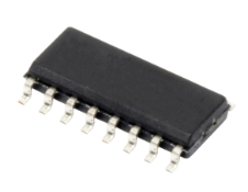
Analog Devices Inc.LDO, FIXED, 3.3V, 0.2A, TSOT-5; Output Type: Fixed; Input Voltage Min: 2.7V; Input Voltage Max: 40V; Fixed Output Voltage Nom.: 3.3V; Adjustable Output Voltage Min: -; Adjustable Output Voltage Max: -; Output Current: 200mA; Dropout Voltage Vdo: 200mV; LDO Regulator Case Style: TSOT; No. of Pins: 5Pins; Operating Temperature Min: -40°C; Operating Temperature Max: 125°C; Product Range: 3.3V 200mA LDO Voltage Regulators; Automotive Qualification Standard: -; RoHS Phthalates Compliant: Yes; MSL: -; SVHC: No SVHC (07-Jul-2017)
HMC451LP3E
Part Number : HMC451LP3E
Analog Devices Inc.RF Amplifier GaAs PHEMT MMIC Med PA, 5 - 18 GHz
LTM4650AIY-1
Part Number : LTM4650AIY-1
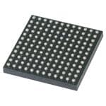
Analog Devices Inc.SWITCHING REGULATOR, CURRENT-MODE, 780KHZ SWITCHING FREQ-MAX, PBGA144
OP284FSZ
Part Number : OP284FSZ
Analog Devices Inc.The OP184/OP284/OP484 are single, dual and quad single-supply, 4 MHz bandwidth amplifiers featuring rail-to-rail inputs and outputs. They are guaranteed to operate from +3 to +36 (or ±1.5 to ±18) volts and will function with a single supply as low as +1.5 volts.These amplifiers are superb for single supply applications requiring both ac and precision dc performance. The combination of bandwidth, low noise and precision makes the OP184/OP284/ OP484 useful in a wide variety of applications, including filters and instrumentation.Other applications for these amplifiers include portable telecom equipment, power supply control and protection, and as amplifiers or buffers for transducers with wide output ranges. Sensors requiring a rail-to-rail input amplifier include Hall effect, piezo electric, and resistive transducers.The ability to swing rail-to-rail at both the input and output enables designers to build multistage filters in single-supply systems and to maintain high signal-to-noise ratios.The OP184/OP284/OP484 are specified over the HOT extended industrial (-40°C to +125°C) temperature range. The single and dual are available in 8-pin plastic DIP plus SO surface mount packages. The quad OP484 is available in 14-pin plastic DIPs and 14-lead narrow-body SO packages.
OP296GSZ
Part Number : OP296GSZ
Analog Devices Inc.The OP196 family of CBCMOS operational amplifiers features micropower operation and rail-to-rail input and output ranges.The extremely low power requirements and guaranteed operation from +3 V to +12 V make these amplifiers perfectly suited to monitor battery usage and to control battery charging. Their dynamic performance, including 26 nV/(root)Hz voltage noise density, recommends them for battery-powered audio applications. Capacitive loads to 200 pF are handled without oscillation.The OP196/OP296/OP496 are specified over the HOT extended industrial (-40°C to +125°C) temperature range. +3 V operation is specified over the 0°C to +125°C temperature range. The single OP196 and the dual OP296 are available in 8-pin plastic DIP and SO-8 surface mount packages. The quad OP496 is available in 14-pin plastic DIP and narrow SO-14 surface mount packages. Check factory for availability of the OP296 and OP496 in the TSSOP package.
REF01HZ
Part Number : REF01HZ
Analog Devices Inc.The REF01 / REF02 / REF03 series of precision voltage references provide a stable 10.0 V, 5.0 V, or 2.5 V output with minimal change in response to variations in supply voltage, ambient temperature or load conditions. The devices are available in 8-lead SOIC, PDIP, CERDIP, and TO-99 packages, as well as 20-terminal LCC packages (883 only), furthering the usability of the devices in both standard and high stress applications.With an external buffer and a simple resistor network, the TEMP terminal can be used for temperature sensing and approximation. A TRIM terminal is also provided on the device for fine adjustment of the output voltage.The small footprint, wide supply range, and application versatility make the REF0x series of references ideal for general-purpose and space-constrained applications.Newer designs should use the ADR01 / ADR02 / ADR03 / ADR06 series of references, which offer higher accuracy and temperature stability over a wider operating temperature range, while maintaining full pin-for-pin compatibility with the REF01 / REF02 / REF03 series. This data sheet applies to commercial-grade products only. Contact sales or visit analog.com for military-grade (883) data sheets.APPLICATIONS Precision data systems High resolution converters Industrial process control systems Precision instruments Military and aerospace applications
REF02AJ/883C
Part Number : REF02AJ/883C
Analog Devices Inc.The REF01 / REF02 / REF03 series of precision voltage references provide a stable 10.0 V, 5.0 V, or 2.5 V output with minimal change in response to variations in supply voltage, ambient temperature or load conditions. The devices are available in 8-lead SOIC, PDIP, CERDIP, and TO-99 packages, as well as 20-terminal LCC packages (883 only), furthering the usability of the devices in both standard and high stress applications.With an external buffer and a simple resistor network, the TEMP terminal can be used for temperature sensing and approximation. A TRIM terminal is also provided on the device for fine adjustment of the output voltage.The small footprint, wide supply range, and application versatility make the REF0x series of references ideal for general-purpose and space-constrained applications.Newer designs should use the ADR01 / ADR02 / ADR03 / ADR06 series of references, which offer higher accuracy and temperature stability over a wider operating temperature range, while maintaining full pin-for-pin compatibility with the REF01 / REF02 / REF03 series. This data sheet applies to commercial-grade products only. Contact sales or visit analog.com for military-grade (883) data sheets.APPLICATION Precision data systems High resolution converters Industrial process control systems Precision instruments Military and aerospace applications Table 1. Selection Guide Device Number Output Voltage Input Voltage Range REF01 10.0 V 12 V to 36 V REF02 5.0 V 7.0 V to 36 V REF03 2.5 V 4.5 V to 36 V
REF194ESZ
Part Number : REF194ESZ
Analog Devices Inc.The REF19x series precision band gap voltage references use a patented temperature drift curvature correction circuit and laser trimming of highly stable, thin-film resistors to achieve a very low temperature coefficient and high initial accuracy.The REF19x series is made up of micropower, low dropout voltage (LDV) devices, providing stable output voltage from supplies as low as 100 mV above the output voltage and consuming less than 45 μA of supply current. In sleep mode, which is enabled by applying a low TTL or CMOS level to the SLEEP pin, the output is turned off and supply current is further reduced to less than 15 μA.The REF19x series references are specified over the extended industrial temperature range (−40°C to +85°C) with typical performance specifications over −40°C to +125°C for applications, such as automotive.All electrical grades are available in an 8-lead SOIC package; the PDIP and TSSOP packages are available only in the lowest electrical grade.APPLICATIONS Portable instruments ADCs and DACs Smart sensors Solar powered applications Loop-current-powered instruments
REF195ESZ
Part Number : REF195ESZ
Analog Devices Inc.The REF19x series precision band gap voltage references use a patented temperature drift curvature correction circuit and laser trimming of highly stable, thin-film resistors to achieve a very low temperature coefficient and high initial accuracy.The REF19x series is made up of micropower, low dropout voltage (LDV) devices, providing stable output voltage from supplies as low as 100 mV above the output voltage and consuming less than 45 μA of supply current. In sleep mode, which is enabled by applying a low TTL or CMOS level to the SLEEP pin, the output is turned off and supply current is further reduced to less than 15 μA.The REF19x series references are specified over the extended industrial temperature range (−40°C to +85°C) with typical performance specifications over −40°C to +125°C for applications, such as automotive.All electrical grades are available in an 8-lead SOIC package; the PDIP and TSSOP packages are available only in the lowest electrical grade.APPLICATIONS Portable instruments ADCs and DACs Smart sensors Solar powered applications Loop-current-powered instruments
SDC1742-411B
Part Number : SDC1742-411B
Analog Devices Inc.The SDC1742 is a hybrid 12-bit continuous tracking synchro digitalconverter. In the core of this hybrid, the conversion process is performedby a monolithic IC manufactured in Analog Devices proprietary BiMOS IIprocess that combines the advantages of CMOS logic and bipolar high accuracy linear circuits on the same chip. Internal isolating micro-transformers are used to provide true isolation of the signal and reference inputs. The 12-bit digital word is in a three-state digital form available in two bytes. Using separate ENABLE inputs for the most significant 8 bits and the least significant 6 or 4 bits not only simplifies multiplexing off more than one device onto a single data bus, but also enables the INHIBIT input to be used without interrupting the operation of tracking loop. The converters are hermetically sealed in a 32-pin welded metal package.
SSM2142SZ
Part Number : SSM2142SZ
Analog Devices Inc.The SSM2142 is an integrated differential-output buffer amplifier that converts a single-ended input signal to a balanced output signal pair with high output drive. By utilizing low noise thermally matched thin film resistors and high slew rate amplifiers, the SSM2142 helps maintain the sonic quality of audio systems by eliminating power line hum, RF interference, voltage drops, and other externally generated noise commonly encountered with long audio cable runs. Excellent rejection of common-mode noise and offset errors is achieved by laser trimming of the onboard resistors, assuring high gain accuracy. The carefully designed output stage of the SSM2142 is capable of driving difficult loads, yielding low distortion performance despite extremely long cables or loads as low as 600 Ohm, and is stable over a wide range of operating conditions.Based on a cross-coupled, electronically balanced topology, the SSM2142 mimics the performance of fully balanced transformer-based solutions for line driving. However, the SSM2142 maintains lower distortion and occupies much less board space than transformers while achieving comparable common-mode rejection performance with reduced parts count.The SSM2142 in tandem with the SSM2141 differential receiver establishes a complete, reliable solution for driving and receiving audio signals over long cables. The SSM2141 features an Input Common-Mode Rejection Ratio of 100 dB at 60 Hz. Specifications demonstrating the performance of this typical system are included in the data sheet.APPLICATIONS Audio Mix Consoles Distribution Amplifiers Graphic and Parametric Equalizers Dynamic Range Processors Digital Effects Processors Telecommunications Systems Industrial Instrumentation Hi-Fi Equipment
SSM2166SZ-REEL
Part Number : SSM2166SZ-REEL
Analog Devices Inc.The SSM2166 integrates a complete and flexible solution for conditioning microphone inputs in computer audio systems. It is also excellent for improving vocal clarity in communications and public address systems. A low noise, voltage-controlled amplifier (VCA) provides a gain that is dynamically adjusted by a control loop to maintain a set compression characteristic. The compression ratio is set by a single resistor and can be varied from 1:1 to over 15:1 relative to a user-defined rotation point; signals above the rotation point are limited to prevent overload and to eliminate popping. In the 1:1 compression setting, the SSM2166 can be programmed with a fixed gain of up to 20 dB; this gain is in addition to the variable gain in other compression settings. The input buffer can also be configured for front-end gains of 0 dB to 20 dB. A downward expander (noise gate) prevents amplification of noise or hum. This results in optimized signal levels prior to digitization, thereby eliminating the need for additional gain or attenuation in the digital domain that could add noise or impair accuracy of speech recognition algorithms. The compression ratio and time constants are set externally. A high degree of flexibility is provided by the VCA gain, rotation point, and noise gate adjustment pins.The SSM2166 is an ideal companion product for audio codecs used in computer systems. The SSM2166 is available in a 14-lead SOIC package and is guaranteed for operation over the extended industrial temperature range of −40°C to +85°C.Applications Microphone preamplifiers/processors Computer sound cards Public address/paging systems Communication headsets Telephone conferencing Guitar sustain effects generators Computerized voice recognition Surveillance systems Karaoke and DJ mixers
AD2S99APZ
Part Number : AD2S99APZ
Analog Devices Inc.The AD2S99 programmable sinusoidal oscillator provides sine wave excitation for resolvers and a wide variety of ac transducers.The AD2S99 also provides a synchronous reference output signal (3 VP-P square wave) that is phase locked to its SIN and COS inputs. In an application, the SIN and COS inputs are connected to the transducer’s secondary windings. The synchronous reference output compensates for temperature and cabling dependent phase shifts and eliminates the need for external preset phase compensation circuits. The synchronous reference output can be used as a zero crossing reference for resolver-to-digital converters such as Analog Devices’ AD2S80A, AD2S82A, AD2S83 and AD2S90.The AD2S99 is packaged in a 20-pin PLCC and operates over –40ºC to +85ºC.PRODUCT HIGHLIGHTS Dynamic Phase Compensation The AD2S99 dynamically compensates for any phase variation in a transducer by phase locking its synchronous reference output to the transducer’s secondary windings. Programmable Excitation Frequency The excitation frequency is easily programmed to 2 kHz, 5 kHz, 10 kHz, or 20 kHz by using the frequency select pins. Intermediate frequencies are available by adding an external resistor. Signal Loss Detection The AD2S99 has the ability to detect if both the transducer secondary winding connections become disconnected from its SIN and COS inputs. The “LOS” output pin pulls high when a signal loss is detected. Integration The AD2S99 integrates the transducer excitation, synchronous reference, and loss of signal detection functions into a small, cost effective package.APPLICATIONSExcitation Source for: Resolvers Synchros LVDTs RVDTs Pressure Transducers Load Cells AC Bridges
AD2S99BPZ
Part Number : AD2S99BPZ
Analog Devices Inc.The AD2S99 programmable sinusoidal oscillator provides sine wave excitation for resolvers and a wide variety of ac transducers.The AD2S99 also provides a synchronous reference output signal (3 VP-P square wave) that is phase locked to its SIN and COS inputs. In an application, the SIN and COS inputs are connected to the transducer’s secondary windings. The synchronous reference output compensates for temperature and cabling dependent phase shifts and eliminates the need for external preset phase compensation circuits. The synchronous reference output can be used as a zero crossing reference for resolver-to-digital converters such as Analog Devices’ AD2S80A, AD2S82A, AD2S83 and AD2S90.The AD2S99 is packaged in a 20-pin PLCC and operates over –40ºC to +85ºC.PRODUCT HIGHLIGHTS Dynamic Phase Compensation The AD2S99 dynamically compensates for any phase variation in a transducer by phase locking its synchronous reference output to the transducer’s secondary windings. Programmable Excitation Frequency The excitation frequency is easily programmed to 2 kHz, 5 kHz, 10 kHz, or 20 kHz by using the frequency select pins. Intermediate frequencies are available by adding an external resistor. Signal Loss Detection The AD2S99 has the ability to detect if both the transducer secondary winding connections become disconnected from its SIN and COS inputs. The “LOS” output pin pulls high when a signal loss is detected. Integration The AD2S99 integrates the transducer excitation, synchronous reference, and loss of signal detection functions into a small, cost effective package.APPLICATIONSExcitation Source for: Resolvers Synchros LVDTs RVDTs Pressure Transducers Load Cells AC Bridges
AD5160BRJZ10-RL7
Part Number : AD5160BRJZ10-RL7
Analog Devices Inc.The AD5160 provides a compact 2.9 mm × 3 mm packaged solution for 256-position adjustment applications. These devices perform the same electronic adjustment function as mechanical potentiometers1 or variable resistors but with enhanced resolution, solid-state reliability, and superior low temperature coefficient performance.The wiper settings are controllable through an SPI-compatible digital interface. The resistance between the wiper and either end point of the fixed resistor varies linearly with respect to the digital code transferred into the RDAC latch.Operating from a 2.7 V to 5.5 V power supply and consuming less than 5 μA allows for usage in portable battery-operated applications.
AD524AD
Part Number : AD524AD
Analog Devices Inc.The AD524 is a precision monolithic instrumentation amplifier designed for data acquisition applications requiring high accuracy under worst-case operating conditions. An outstanding combination of high linearity, high common mode rejection, low offset voltage drift, and low noise makes the AD524 suitable for use in many data acquisition systems.The AD524 has an output offset voltage drift of less than 25 µV/ °C, input offset voltage drift of less than 0.5 µV/°C, CMR above 90 dB at unity gain (120 dB at G = 1000) and maximum nonlinearity of 0.003% at G = 1. In addition to the outstanding dc specifications the AD524 also has a 25MHz gain bandwidth product (G = 1000). To make it suitable for high speed data ac-quisition systems the AD524 has an output slew rate of 5 V/µs and settles in 15µs to 0.01% for gains of 1 to 100.As a complete amplifier the AD524 does not require any external components for fixed gains of 1, 10, 100 and 1,000. For other gain settings between 1 and 1000 only a single resistor is required. The AD524 input is fully protected for both power on and power off fault conditions.The AD524 IC instrumentation amplifier is available in four different versions of accuracy and operating temperature range. The economical 'A' grade, the low drift 'B' grade and lower drift, higher linearity 'C' grade are specified from -25°C to +85°C. The 'S' grade guarantees performance to specification over the extended temperature range -55°C to +125°C. Devices are available in 16-pin ceramic DIP and SOIC packages and a 20-terminal leadless chip carrier.Product HighlightsThe AD524 has guaranteed low offset voltage, offset voltage drift, and low noise for precision high gain applications. The AD524 is functionally complete with pin program- mable gains of 1, 10, 100, and 1000, and single resistor programmable for any gain. Input and output offset nulling terminals are provided for very high precision applications and to minimize offset voltage changes in gain ranging applications. The AD524 is input protected for both power-on and power-off fault conditions. The AD524 offers superior dynamic performance with a gain bandwidth product of 25 MHz, full power response of 75 kHz and a settling time of 15 μs to 0.01% of a 20 V step (G = 100). Data Sheet, Rev. F, 11/07
AD5382BSTZ-5
Part Number : AD5382BSTZ-5
Analog Devices Inc.The AD5382 is a 32-channel, 14-Bit DAC and is available in a 14 mm × 14 mm 100-lead LQFP package. It operates from a single 3 V or 5 V supply. Programmable gain (m) and offset (c) are provided per channel to facilitate system calibration. Each DAC channel is double-buffered which allows all DAC outputs to be updated simultaneously via an LDAC pin. Each channel has an on-chip output amplifier which allows rail-to-rail operation. The AD5382 includes an internal 1.25 V/2.5 V low-drift reference. The AD5382 contains a parallel interface with a WR pulse width of 20 ns, a 30 MHz SPI interface and a 400 kHz I2C-compatible interface.This device is pin-to-pin compatible with the AD5380 (40-ch 14-bit DAC), the AD5381 (40-ch 12-bit DAC) and the AD5383 (32-ch 12-bit DAC).APPLICATIONS Variable optical attenuators (VOAs) Level setting (ATE) Optical micro-electro-mechanical systems (MEMS) Control systems Instrumentation
AD5445YRUZ-REEL7
Part Number : AD5445YRUZ-REEL7
Analog Devices Inc.The AD5424 / AD5433 / AD5445 are CMOS 8-, 10-, and 12-bitcurrent output digital-to-analog converters (DACs), respectively.These devices operate from a 2.5 V to 5.5 V power supply,making them suitable for battery-powered applications andmany other applications. These DACs utilize data readback,allowing the user to read the contents of the DAC register viathe DB pins. On power-up, the internal register and latches arefilled with 0s and the DAC outputs are at zero scale.As a result of manufacturing with a CMOS submicron process,they offer excellent 4-quadrant multiplication characteristics,with large signal multiplying bandwidths of up to 10 MHz.The applied external reference input voltage (VREF) determines thefull-scale output current. An integrated feedback resistor (RFB)provides temperature tracking and full-scale voltage outputwhen combined with an external I-to-V precision amplifier.While these devices are upgrades of the AD5424 / AD5433 /AD5445 in multiplying bandwidth performance, they have alatched interface and cannot be used in transparent mode.The AD5424 is available in a small, 20-lead LFCSP and a small,16-lead TSSOP, while the AD5433 and AD5445 DACs are availablein a small, 20-lead LFCSP and a small, 20-lead TSSOP.The EVAL-AD5445SDZ evaluation board is available forevaluating DAC performance. For more information, see theUG-333 evaluation board user guide.APPLICATIONS Portable battery-powered applications Waveform generators Analog processing Instrumentation applications Programmable amplifiers and attenuators Digitally controlled calibration Programmable filters and oscillators Composite video Ultrasound Gain, offset, and voltage trimming
AD574AKD
Part Number : AD574AKD
Analog Devices Inc.The AD574A is a complete 12-bit successive-approximation analog-to-digital converter with 3-state output buffer circuitry for direct interface to an 8- or 16-bit microprocessor bus. A high precision voltage reference and clock are included on-chip, and the circuit guarantees full-rated performance without external circuitry or clock signals.The AD574A design is implemented using Analog Devices' Bipolar/I2L process, and integrates all analog and digital functions on one chip. Offset, linearity and scaling errors are minimized by active laser-trimming of thin-film resistors at the wafer stage. The voltage reference uses an implanted buried Zener for low noise and low drift. On the digital side, I2L logic is used for the successive-approximation register, control circuitry and 3-state output buffers.The AD574A is available in six different grades. The AD574AJ, K, and L grades are specified for operation over the 0°C to +70°C temperature range. The AD574AS, T, and U are specified for the -55°C to +125°C range. All grades are available in a 28-pin hermetically-sealed ceramic DIP. Also, the J, K, and L grades are available in a 28-pin plastic DIP and PLCC, and the J and K grades are available in ceramic LCC.The S, T, and U grades in ceramic DIP or LCC are available with optional processing to MIL-STD-883C Class B; the T and U grades are available as JAN QPL. The Analog Devices' Military Products Databook should be consulted for details on /883B testing of the AD574A.
AD625ADZ
Part Number : AD625ADZ
Analog Devices Inc.The AD625 is a precision instrumentation amplifier specifically designed to fulfill two major areas of application: 1) Circuits requiring nonstandard gains (i.e., gains not easily achievable with devices such as the AD524 and AD624). 2) Circuits requiring a low cost, precision software programmable gain amplifier.For low noise, high CMRR, and low drift the AD625JN is the most cost effective instrumentation amplifier solution available. An additional three resistors allow the user to set any gain from 1 to 10,000. The error contribution of the AD625JN is less than 0.05% gain error and under 5 ppm/°C gain TC; performance limitations are primarily determined by the external resistors. Common-mode rejection is independent of the feedback resistor matching.A software programmable gain amplifier (SPGA) can be configured with the addition of a CMOS multiplexer (or other switch network), and a suitable resistor network. Because the ON resistance of the switches is removed from the signal path, an AD625 based SPGA will deliver 12-bit precision, and can be programmed for any set of gains between 1 and 10,000, with completely user selected gain steps.For the highest precision the AD625C offers an input offset voltage drift of less than 0.25 µV/°C, output offset drift below 15 µV/°C, and a maximum nonlinearity of 0.001% at G = 1. All grades exhibit excellent ac performance; a 25 MHz gain bandwidth product, 5 V/µs slew rate and 15 µs settling time.The AD625 is available in three accuracy grades (A, B, C) for industrial (-40°C to +85°C) temperature range, two grades (J, K) for commercial (0°C to +70°C) temperature range, and one (S) grade rated over the extended (-55°C to +125°C) temperature range.


