ADM3307EACPZ
Part Number : ADM3307EACPZ
Analog Devices Inc.Operating from a single supply as low as +2.7 V, the ADM3307E is a five-driver/three-receiver serial port transceiver, and fully meets full EIA-232 standards. It features an on-board, charge pump dc-to-dc converter, which eliminates the need for dual power supplies. This dc-to-dc converter also contains a voltage tripler and voltage inverter for internally generating positive and negative supplies from the power supply. It operates in Green Idle Mode, where the charge pump oscillator is gated on and off to maintain output voltage to +/-7.25 V, regardless of the load conditions. It has the added benefit of having +15kV ESD protection on both the RS-232 I/O pins and the TTL pins, making it ideal for harsh environments. It also operates at speeds of up to 1Mbps. The ADM3307E is available in a 28-pin TSSOP package as well as a space-saving 32-pin LFCSP package.APPLICATIONS Mobile phone handsets/data cables Laptop and notebook computers Printers Peripherals Modems PDAs/Hand-Held Devices/Palmtop Computers
ADM3312EACPZ
Part Number : ADM3312EACPZ
Analog Devices Inc.The ADM3312E is a three-driver/three-receiver serial port transceiver, which meets full EIA-232 standards while operating from a single power supply as low as +2.7V. It features an on-board, charge pump dc-to-dc converter, which eliminates the need for dual power supplies. This dc-to-dc converter also contains a voltage tripler and voltage inverter for internally generating positive and negative supplies from the power supply. It operates in Green Idle Mode, where the charge pump oscillator is gated on and off to maintain output voltage to +/-7.25 V, regardless of the load conditions. Another key feature is its ESD protection: up to +/-15kV on all I/O lines. The ADM3312E is available in a 24-pin TSSOP package as well as a space-saving 32-pin LFCSP package.APPLICATIONS Mobile phone handsets/data cables Laptop and notebook computers Printers Peripherals Modems PDAs/Hand-Held Devices/Palmtop Computers
ADM696SQ
Part Number : ADM696SQ
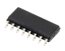
Analog Devices Inc.The ADM696 / ADM697 supervisory circuits offer complete single chip solutions for power supply monitoring and battery control functions in microprocessor systems. These functions include µP reset, backup-battery switchover, watchdog timer, CMOS RAM write protection, and power failure warning.The ADM696 / ADM697 are available in 16-pin DIP and small outline packages and provide the following functions: Power-On Reset output during power-up, power-down and brownout conditions. The RESET voltage threshold is adjustable using an external voltage divider. The RESET output remains operational with VCC as low as 1 V. A Reset pulse if the optional watchdog timer has not been toggled within specified time. Separate watchdog time-out and low line status outputs. Adjustable reset and watchdog timeout periods. A 1.3 V threshold detector for power fail warning, low battery detection, or to monitor a power supply other than VCC. Battery backup switching for CMOS RAM, CMOS micro-processor or other low power logic (ADM696). Write protection of CMOS RAM or EEPROM (ADM697).The ADM696 / ADM697 is fabricated using an advanced epitaxial CMOS process combining low power consumption (5 mW), extremely fast Chip Enable gating (5 ns) and high reliability. RESET assertion is guaranteed with VCC as low as 1 V. In addition, the power switching circuitry is designed for minimal voltage drop thereby permitting increased output current drive of up to 100 mA without the need for an external pass transistor.
ADM697ARZ
Part Number : ADM697ARZ
Analog Devices Inc.The ADM696 / ADM697 supervisory circuits offer complete single chip solutions for power supply monitoring and battery control functions in microprocessor systems. These functions include µP reset, backup-battery switchover, watchdog timer, CMOS RAM write protection, and power failure warning.The ADM696 / ADM697 are available in 16-pin DIP and small outline packages and provide the following functions: Power-On Reset output during power-up, power-down and brownout conditions. The RESET voltage threshold is adjustable using an external voltage divider. The RESET output remains operational with VCC as low as 1 V. A Reset pulse if the optional watchdog timer has not been toggled within specified time. Separate watchdog time-out and low line status outputs. Adjustable reset and watchdog timeout periods. A 1.3 V threshold detector for power fail warning, low battery detection, or to monitor a power supply other than VCC. Battery backup switching for CMOS RAM, CMOS micro-processor or other low power logic (ADM696). Write protection of CMOS RAM or EEPROM (ADM697).The ADM696 / ADM697 is fabricated using an advanced epitaxial CMOS process combining low power consumption (5 mW), extremely fast Chip Enable gating (5 ns) and high reliability. RESET assertion is guaranteed with VCC as low as 1 V. In addition, the power switching circuitry is designed for minimal voltage drop thereby permitting increased output current drive of up to 100 mA without the need for an external pass transistor.
ADN2813ACPZ
Part Number : ADN2813ACPZ
Analog Devices Inc.The ADN2813 provides the receiver functions of quantization, signal level detect, and clock and data recovery for continuous data rates from 12.3 Mb/s to 1.25 Gb/s. The ADN2813 automatically locks to all data rates without the need for an external reference clock or programming. All SONET jitter requirements are met, including jitter transfer, jitter generation, and jitter tolerance. All specifications are quoted for −40°C to+85°C ambient temperature, unless otherwise noted.This device, together with a PIN diode and a TIA preamplifier, can implement a highly integrated, low cost, low power fiber optic receiver.The receiver front end loss of signal (LOS) detector circuit indicates when the input signal level has fallen below a useradjustable threshold. The LOS detect circuit has hysteresis to prevent chatter at the output.The ADN2813 is available in a compact 5 mm × 5 mm 32-lead chip scale package.ApplicationsSONET OC-1/3/12 and all associated FEC rates Fibre Channel, GbE, HDTV, etc.WDM transpondersRegenerators/repeatersTest equipmentBroadband cross-connects and routers
ADSP-BF536BBCZ-3B
Part Number : ADSP-BF536BBCZ-3B
Analog Devices Inc.The Blackfin® Processor family has been expanded to address the ever-increasing need for pervasive embedded network connectivity. This connectivity is powerful when utilized in conjunction with the high performance 16-/32-bit Blackfin embedded processor core, the flexible cache architecture, the enhanced DMA subsystem, and the Dynamic Power Management (DPM) functionality. System designers can take advantage of the combined control and signal processing capabilities of the processor core across a wide range of end applications through the scalability of the pin and code compatibility of these new family members. The ADSP-BF536 and ADSP-BF537 are a functional extension of the popular ADSP-BF531 / ADSP-BF532 / ADSP-BF533 processors, and they are ideally suited for a variety of networked applications. The ADSP-BF537 is the higher performance series member, with more embedded memory enabling higher throughput needs for embedded applications suchas video security/surveillance and industrial-environment-based distributed control/factory automation applications. The ADSP-BF536 offers exceptional performance and is designed for low cost connected devices such as remote monitoring devices, VoIP, point-of-sale terminals, and biometrics/security applications. Both devices are ideally suited for a broadrange of industrial, instrumentation, medical, and consumer appliance applications— allowing for scalability based upon the required network bandwidth and mix of control, plus signal processing needed in the end product.
ADUC845BSZ62-5
Part Number : ADUC845BSZ62-5
Analog Devices Inc.The ADuC845, ADuC847, and ADuC848 are single-cycle,12.58 MIPs, 8052 core upgrades to the ADuC834 andADuC836. They include additional analog inputs forapplications requiring more ADC channels.The ADuC845, ADuC847, and ADuC848 are complete smarttransducer front ends. The family integrates high resolutionΣ-Δ ADCs with flexible, up to 10-channel, input multiplexing, afast 8-bit MCU, and program and data Flash/EE memory on asingle chip.The ADuC845 includes two (primary and auxiliary) 24-bit Σ-ΔADCs with internal buffering and PGA on the primary ADC.The ADuC847 includes the same primary ADC as the ADuC845(auxiliary ADC removed). The ADuC848 is a 16-bit ADCversion of the ADuC847.The ADCs incorporate flexible input multiplexing, a temperaturesensor (ADuC845 only), and a PGA (primary ADC only)allowing direct measurement of low-level signals. The ADCsinclude on-chip digital filtering and programmable output datarates that are intended for measuring wide dynamic range andlow frequency signals, such as those in weigh scale, strain gage,pressure transducer, or temperature measurement applications.The devices operate from a 32 kHz crystal with an on-chip PLLgenerating a high frequency clock of 12.58 MHz. This clock isrouted through a programmable clock divider from which theMCU core clock operating frequency is generated. The microcontrollercore is an optimized single-cycle 8052 offering up to12.58 MIPs performance while maintaining 8051 instruction setcompatibility.The available nonvolatile Flash/EE program memory optionsare 62 kbytes, 32 kbytes, and 8 kbytes. 4 kbytes of nonvolatileFlash/EE data memory and 2304 bytes of data RAM are alsoprovided on-chip. The program memory can be configured asdata memory to give up to 60 kbytes of NV data memory indata logging applications.On-chip factory firmware supports in-circuit serial downloadand debug modes (via UART), as well as single-pin emulationmode via the EA pin. The ADuC845, ADuC847, and ADuC848are supported by the QuickStart™ development system featuringlow cost software and hardware development tools.Applications Multichannel sensor monitoring Industrial/environmental instrumentation Weigh scales, pressure sensors, temperature monitoring Portable instrumentation, battery-powered systems Data logging, precision system monitoring
ADV7125BCPZ170
Part Number : ADV7125BCPZ170
Analog Devices Inc.The ADV7125 (ADV®) is a triple high speed, digital-to-analogconverter (DAC) on a single monolithic chip. It consists of threehigh speed, 8-bit video DACs with complementary outputs, astandard TTL input interface, and a high impedance, analogoutput current source.The ADV7125 has three separate 8-bit-wide input ports. Asingle +5 V/+3.3 V power supply and clock are all that arerequired to make the device functional. The ADV7125 hasadditional video control signals, composite SYNC and BLANKas well as a power save mode.The ADV7125 is fabricated in a 5 V CMOS process. Itsmonolithic CMOS construction ensures greater functionalitywith lower power dissipation. The ADV7125 is available in 48-lead LQFP and 48-lead LFCSP packages.Product Highlights 330 MSPS (3.3 V only) throughput. Guaranteed monotonic to eight bits. Compatible with a wide variety of high resolution color graphics systems, including RS-343A and RS-170.Applications Digital video systems High resolution color graphics Digital radio modulation Image processing Instrumentation Video signal reconstruction Automotive infotainment units
ADV7179BCPZ
Part Number : ADV7179BCPZ
Analog Devices Inc.The ADV7179 is suitable for a wide range of video applications such as 3rd generation mobile phones or digital still cameras for video output functionality where package space is as a premium.The ADV7179 comes in a compact chip-scale package, measuring just 6mm by 6mm square, with options for CCIR656 standard video input, with or without embedded timing information.Video performance is not compromised. Advanced filtering (SSAF filters) and professional-level video SNR up to -80dB provides for excellent display quality in a compact format.For more information, download the datasheet today using the links on the left.APPLICATIONS Portable video applications Mobile phones Digital still cameras
DC1053A-H
Part Number : DC1053A-H
Analog Devices Inc.The LTC3526/LTC3526B are synchronous, fixed frequency step-up DC/DC converters with output disconnect. Synchronous rectification enables high efficiency in the low profile 2mm × 2mm DFN package. Battery life in single AA/AAA powered products is extended further with an 850mV start-up voltage and operation down to 500mV once started.A switching frequency of 1MHz minimizes solution footprint by allowing the use of tiny, low profile inductors and ceramic capacitors. The current mode PWM design is internally compensated, reducing external parts count. The LTC3526 features automatic Burst Mode operation at light load conditions, while the LTC3526B features continuous switching at light loads. Anti-ringing control circuitry also reduces EMI concerns by damping the inductor in discontinuous mode. Additional features include a low shutdown current of under 1μA and thermal shutdown.The LTC3526/LTC3526B are housed in a 2mm × 2mm × 0.75mm DFN package.For new designs, we recommend the LTC3526L/LTC3526LB. Startup Voltage Frequency Burst Mode Notes LTC3526 1V 1MHz Yes Not Recommended For New Designs LTC3526B 1V 1MHz No Not Recommended For New Designs LTC3526-2 1V 2MHz Yes Not Recommended For New Designs LTC3526B-2 1V 2MHz No Not Recommended For New Designs LTC3526L 0.85V 1MHz Yes LTC3526LB 0.85V 1MHz No LTC3526L-2 0.85V 2MHz Yes LTC3526LB-2 0.85V 2MHz No APPLICATIONS Medical Instruments Flash-Based MP3 Players Noise Canceling Headphones Wireless Mice Bluetooth Headsets
DC981A/B
Part Number : DC981A/B
Analog Devices Inc.The LTC4263 is an autonomous single-channel PSE controller for use in IEEE 802.3af compliant Power over Ethernet systems. It includes an on-board power MOSFET, internal inrush, current limit, and short-circuit control, IEEE 802.3af compliant PD detection and classification circuitry, and selectable AC or DC disconnect sensing. On-board control algorithms provide complete IEEE 802.3af compliant operation without the need of a microcontroller. The LTC4263 simplifies PSE implementation, needing only a single 48V supply and a small number of passive support components.Programmable on-board power management circuitry permits multiple LTC4263s to allocate and share power in multi-port systems, allowing maximum utilization of the 48V power supply—all without the intervention of a host processor. The port current limit can be configured to automatically adjust to the detected PD class. Detection back-off timing is configurable for either Endpoint or Midspan operation. Built-in foldback and thermal protection provide comprehensive fault protection.An LED pin indicates the state of the port controlled by the LTC4263. When run from a single 48V supply, the LED pin can operate as a simple switching current source to reduce power dissipation in the LED drive circuitry.The LTC4263 is available in 14-pin 4mm × 3mm DFN and 14-pin SO packages.Applications IEEE 802.3af Compliant Endpoint/Midspan PSEs Single-Port or Multi-Port Power Injectors Power Forwarders Low-Port Count PSEs Environment B PSEs Standalone PSEs
EVAL-ADCMP573BCPZ
Part Number : EVAL-ADCMP573BCPZ
Analog Devices Inc.The ADCMP572 and ADCMP573 are ultrafast comparators fabricated on Analog Devices’ proprietary XFCB3 Silicon Germanium (SiGe) bipolar process. The ADCMP572 features CML output drivers and latch inputs, and the ADCMP573 features reduced swing PECL (RSPECL) output drivers and latch inputs.Both devices offer 150 ps propagation delay and 80 ps minimum pulse width for 10 Gbps operation with 200 fs rms random jitter (RJ). Overdrive and slew rate dispersion are typically less than 15 ps.A flexible power supply scheme allows both devices to operate with a single 3.3 V positive supply and a −0.2 V to +1.2 V input signal range or with split input/output supplies to support a wider −0.2 V to +3.2 V input signal range and an independent range of output levels. 50 Ω on-chip termination resistors are provided at both inputs with the optional capability to be left open (on an individual pin basis) for applications requiring high impedance inputs.The CML output stage is designed to directly drive 400 mV into 50 Ω transmission lines terminated to between 3.3 V to 5.2 V. The RSPECL output stage is designed to drive 400 mV into 50 Ω terminated to VCCO − 2 V and is compatible with several commonly used PECL logic families. The comparator input stage offers robust protection against large input overdrive, and the outputs do not phase reverse when the valid input signal range is exceeded. High speed latch and programmable hysteresis features are also provided.The ADCMP572 and ADCMP573 are available in a 16-lead LFCSP package and have been characterized over an extended industrial temperature range of −40°C to +125°C.APPLICATIONS Clock and data signal restoration and level shifting Automatic test equipment (ATE) High speed instrumentation Pulse spectroscopy Medical imaging and diagnostics High speed line receivers Threshold detection Peak and zero-crossing detectors High speed trigger circuitry
EVAL-ADG901EBZ
Part Number : EVAL-ADG901EBZ
Analog Devices Inc.The ADG901/ADG902 are wideband switches that use a complementary metal-oxide semiconductor (CMOS) process to provide high isolation and low insertion loss to 1 GHz. The ADG901 is an absorptive (matched) switch with 50 Ω terminated shunt legs, while the ADG902 is a reflective switch. These devices are designed such that the isolation is high over the dc to 1 GHz frequency range. These switches enable the user to pass dc signals up to 0.5 V without the use of a dc blocking capacitor. They have on-board CMOS control logic, thus eliminating the need for external controlling circuitry. The control inputs are both CMOS and LVTTL compatible. The low power consumption of these CMOS devices makes them ideally suited to wireless applications and general-purpose high frequency switching.Product Highlights 40 dB Off Isolation at 1 GHz 0.8 dB Insertion Loss at 1 GHz 17 dBm P1dB at 1 GHzApplications Wireless communications General purpose RF switching Dual-band applications High speed filter selection Digital transceiver front-end switch IF switching Tuner modules Antenna diversity switching list
AD7327BRUZ-REEL
Part Number : AD7327BRUZ-REEL
Analog Devices Inc.The AD73271 is an 8-Channel, 12-Bit plus Sign Successive Approximation ADC designed on the iCMOS (industrial CMOS) process. iCMOS is a process combining high voltage silicon with submicron CMOS and complementary bipolar technologies. It enables the development of a wide range of high performance analog ICs capable of 33 V operation in a footprint that no previous generation of high voltage parts could achieve. Unlike analog ICs using conventional CMOS processes, iCMOS components can accept bipolar input signals while providing increased performance, dramatically reduced power consumption, and reduced package size.The AD7327 can accept true bipolar Analog Input signals. The AD7327 has four software selectable inputs Ranges, ±10 V, ±5 V, ±2.5 V and 0 to 10 V. Each analog input channel can be independently programmed to one of the four input ranges. The Analog input channels on the AD7327 can be programmed to be Single-Ended, true Differential or Pseudo Differential.The ADC contains a 2.5 V Internal reference. The AD7327 also allows for external Reference operation. If a 3 V reference is applied the REFIN/OUT pin the AD7327 can accept a true Bipolar ±12V Analog Input. VDD and VSS supplies of ±12V are required for the ±12 V Input Range. The ADC has a high speed serial interface that can operate at throughput rates up to 500 kSPS.Product Highlights The AD7327 can accept True Bipolar Analog Input signals, ±10 V, ±5 V, ±2.5 V and 0 to 10 V unipolar signals. The Eight Analog Inputs can be configured as 8 Single-Ended inputs, 4 True Differential, 4 Pseudo Differential or 7 Pseudo Differential Inputs. The ADC has a high speed serial interface that can operate at throughput rates up to 500 kSPS. Low power, 18 mW, at a maximum throughput rate of 500 kSPS. Channel Sequencer.
AD7656BSTZ
Part Number : AD7656BSTZ
Analog Devices Inc.The AD7656 / AD7657 / AD7658 contain six 16-/14-/12-bit, fast, low power, successive approximation ADCs all in the one package that is designed on the iCMOS™ process (industrial CMOS). iCMOS is a process combining high voltage silicon with submicron CMOS and complementary bipolar technologies. It enables the development of a wide range of high performance analog ICs, capable of 33 V operation in a footprint that no previous generation of high voltage parts could achieve. Unlike analog ICs using conventional CMOS processes, iCMOS components can accept bipolar input signals while providing increased performance, which dramatically reduces power consumption and package size.The AD7656 / AD7657 / AD7658 feature throughput rates up to 250 kSPS. The parts contain low noise, wide bandwidth, track-and-hold amplifiers that can handle input frequencies up to 12 MHz.The conversion process and data acquisition are controlled using CONVST signals and an internal oscillator. Three CONVST pins allow independent, simultaneous sampling of the three ADC pairs. The AD7656/AD7657/AD7658 all have a high speed parallel and serial interface, allowing the devices to interface with microprocessors or DSPs. In serial interface mode, the parts have a daisy-chain feature that allows multiple ADCs to connect to a single serial interface. The AD7656 / AD7657 / AD7658 can accommodate true bipolar input signals in the ±4 × VREF range and ±2 × VREF range. The AD7656 / AD7657/ AD7658 also contain an on-chip 2.5 V reference.Please visit next generation product AD7606. Recommended for new designs is the AD7656A pin for pin compatible device with improved PSS robustness. For reduced decoupling requirements visit the AD7656-1 or AD7656A-1 product page.PRODUCT HIGHLIGHTS Six 16-/14-/12-bit, 250 kSPS ADCs on board. Six true bipolar, high impedance analog inputs. Parallel and high speed serial interfaces.APPLICATIONS Power line monitoring systems Instrumentation and control systems Multi-axis positioning systems
AD8003ACP-EBZ
Part Number : AD8003ACP-EBZ
Analog Devices Inc.The AD8003 is a triple ultrahigh speed current feedback amplifier. Using ADI’s proprietary eXtra Fast Complementary Bipolar (XFCB) process, the AD8003 achieves a bandwidth of 1.5 GHz and a slew rate of 4300 V/µs. Additionally, the amplifier provides excellent dc precision with an input bias current of 50 µA maximum and a dc input voltage of 0.7 mV.The AD8003 has excellent video specifications with a frequency response that remains flat out to 190 MHz and 0.1% settling within 12 ns to ensure that even the most demanding video systems maintain excellent fidelity. For applications that use NTSC video, as well as high speed video, the amplifier provides a differential gain of 0.05% and a differential gain of 0.01°.The AD8003 amplifier is available in a compact 4 mm × 4 mm, 24-lead LFCSP_VQ. The AD8003 is rated to work over the industrial temperature range of -40°C to +85°C.
AD8021ARMZ
Part Number : AD8021ARMZ
Analog Devices Inc.The AD8021 is an exceptionally high performance, high speed voltage feedback amplifier that can be used in 16-bit resolution systems. It is designed to have both low voltage and low current noise (2.1 nV/√Hz typical and 2.1 pA/√Hz typical) while operating at the lowest quiescent supply current (7 mA @ ±5 V) among today's high speed, low noise op amps. The AD8021 operates over a wide range of supply voltages from ±2.25 V to ±12 V, as well as from single 5 V supplies, making it ideal for high speed, low power instruments. An output disable pin allows further reduction of the quiescent supply current to 1.3 mA.The AD8021 is both technically superior and priced considerably less than comparable amps drawing much higher quiescent current. The AD8021 is a high speed, general-purpose amplifier, ideal for a wide variety of gain configurations, and can be used throughout a signal processing chain and in control loops. The AD8021 is available in both standard 8-lead SOIC and MSOP packages in the industrial temperature range of -40°C to +85°C.
AD8028ARZ
Part Number : AD8028ARZ
Analog Devices Inc.The AD8027/AD8028 are high speed amplifiers with rail-to-railinput and output that operate on low supply voltages and areoptimized for high performance and a wide dynamic signal range.The AD8027/AD8028 have low noise (4.3 nV/√Hz, 1.6 pA/√Hz)and low distortion (120 dBc at 1 MHz). In applications that use afraction of or use the entire input dynamic range and requirelow distortion, the AD8027/AD8028 are ideal choices.Many rail-to-rail input amplifiers have an input stage that switchesfrom one differential pair to another as the input signal crossesa threshold voltage, which causes distortion. The AD8027/AD8028have a unique feature that allows the user to select the inputcrossover threshold voltage through the DISABLE/SELECT pin(DISABLE/SELECT x in the 10-lead MSOP, hereafter referredto as DISABLE/SELECT throughout this data sheet). This featurecontrols the voltage at which the complementary transistorinput pairs switch. The AD8027/AD8028 also have intrinsicallylow crossover distortion.With their wide supply voltage range (2.7 V to 12 V) and widebandwidth (190 MHz), the AD8027/AD8028 amplifiers aredesigned to work in a variety of applications where speed andperformance are needed on low supply voltages. The high performanceof the AD8027/AD8028 is achieved with a quiescentcurrent of only 6.5 mA (typical) per amplifier. The AD8027/AD8028 have a shutdown mode that is controlled viathe DISABLE/SELECT pin.The AD8027/AD8028 are available in 8-lead SOIC, 6-lead SOT-23,and 10-lead MSOP packages. The AD8028WARMZ-R7 is anautomotive grade version, qualified for automotive applications.See the Automotive Products section for more details. TheAD8027/AD8028 family is designed to work over the extendedtemperature range of −40°C to +125°C.Applications Filters ADC drivers Level shifting Buffering Professional video Low voltage instrumentation
AD8042ARZ
Part Number : AD8042ARZ
Analog Devices Inc.The AD8042 is a low power voltage feedback, high speed amplifier designed to operate on +3 V, +5 V or ± 5 V supplies. It has true single supply capability with an input voltage range extending 200 mV below the negative rail and within 1 V of the positive rail.The output voltage swing extends to within 30 mV of each rail, providing the maximum output dynamic range. Additionally, it features gain flatness of 0.1 dB to 14 MHz while offering differential gain and phase error of 0.04% and 0.06° on a single 5 V supply. This makes the AD8042 useful for professional video electronics such as cameras, video switchers or any high speed portable equipment. The AD8042's low distortion and fast settling make it ideal for buffering single-supply, high speed Analog-to-Digital converters (ADCs).The AD8042 offers low power supply current of 12 mA maximum and can run on a single 3.3 V power supply. These features are ideally suited for portable and battery powered applications where size and power are critical.The wide bandwidth of 160 MHz along with 200 V/µs of slew rate on a single 5 V supply make the AD8042 useful in many general-purpose, high speed applications where single supplies from +3.3 V to +12 V and dual power supplies of up to ±6 V are needed. The AD8042 is available in 8-lead PDIP and SOIC_N packages.ApplicationsVideo switchersDistribution amplifiersAnalog-to-digital driversProfessional camerasCCD Imaging systemsUltrasound equipment (multichannel)
AD8065ARZ-REEL
Part Number : AD8065ARZ-REEL
Analog Devices Inc.The AD8065/AD80661 FastFET™ amplifiers are voltage feedback amplifiers with FET inputs offering high performance and ease of use. The AD8065 is a single amplifier, and the AD8066 is a dual amplifier. These amplifiers are developed in the Analog Devices, Inc. proprietary XFCB process and allow exceptionally low noise operation (7.0 nV/√Hz and 0.6 fA/√Hz) as well as very high input impedance.With a wide supply voltage range from 5 V to 24 V, the ability to operate on single supplies, and a bandwidth of 145 MHz, the AD8065/AD8066 are designed to work in a variety of applications. For added versatility, the amplifiers also contain rail-to-rail outputs.Despite the low cost, the amplifiers provide excellent overall performance. The differential gain and phase errors of 0.02% and 0.02°, respectively, along with 0.1 dB flatness out to 7 MHz, make these amplifiers ideal for video applications. Additionally, they offer a high slew rate of 180 V/µs, excellent distortion (SFDR of −88 dBc @ 1 MHz), extremely high common-mode rejection of −100 dB, and a low input offset voltage of 1.5 mV maximum under warmed up conditions. The AD8065/AD8066 operate using only a 6.4 mA/amplifier typical supply current and are capable of delivering up to 30 mA of load current.The AD8065/AD8066 are high performance, high speed, FET input amplifiers available in small packages: SOIC-8, MSOP-8, and SOT-23-5. They are rated to work over the industrial temperature range of −40°C to +85°C.The AD8065WARTZ-R7 is fully qualified for automotive applications. It is rated to operate over the extended temperature range (−40°C to +105°C), up to a maximum supply voltage range of ±5 V onlyApplications Automotive driver assistance systems Photodiode preamps Filters A/D drivers Level shifting Buffering


