AD8403ARZ10
Part Number : AD8403ARZ10
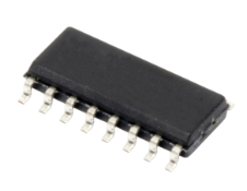
Analog Devices Inc.The AD8400 / AD8402 / AD8403 provide a single, dual or quad channel, 256 position digitally controlled variable resistor (VR) device. These devices perform the same electronic adjustment function as a potentiometer or variable resistor. The AD8400 contains a single variable resistor in the compact SO-8 package. The AD8402 contains two independent variable resistors in saving SO-14 surface mount package. The AD8403 contains four independent variable resistors in 24-lead PDIP, SOIC and TSSOP packages. Each part contains a fixed resistor with a wiper contact that taps the fixed resistor value at a point determined by a digital code loaded into the controlling serial input register. The resistance between the wiper and either endpoint of the fixed resistor varies linearly with respect to the digital code transferred into the VR latch. Each variable resistor offers a completely programmable value of resistance, between the A terminal and the wiper or the B terminal and the wiper. The fixed A to B terminal resistance of 1 kΩ, 10 kΩ, 50 kΩ or 100 kΩ has a ±1% channel-to-channel matching tolerance with a nominal temperature coefficient of 500 ppm/°C. A unique switching circuit minimizes the high glitch inherent in traditional switched resistor designs avoiding any make-before-break or break-before-make operation.Each VR has its own VR latch that holds its programmed resistance value. These VR latches are updated from an SPI compatible serial-to-parallel shift register that is loaded from a standard 3-wire serial-input digital interface. Ten data bits make up the data word clocked into the serial input register. The data word is decoded where the first two bits determine the address of the VR latch to be loaded, the last eight bits are data. A serial data output pin at the opposite end of the serial register allows simple daisy-chaining in multiple VR applications without additional external decoding logic.
AD8651ARZ
Part Number : AD8651ARZ
Analog Devices Inc.The AD8651 and AD8652 are high precision low noise low distortion rail-to-rail CMOS operational amplifiers running at single supply voltage from 2.7V to 5.5V.The single and dual amplifiers are both offered in the 8-Lead SOIC package and the single is also offered in the 8- Lead MSOP package.The AD8651/2 features high speed, high bandwidth, low noise and high precision. They are rail-to-rail output amplifiers with a gain bandwidth of 50 MHz and typical voltage offset of 150uV from a 5V supply. It also featureslow noise of 5nV per square root Hertz.The AD8651/2 can be used in communication areas, such as cell phone transmission power control, fiber optics networking, wireless networking and video line drivers. The AD8651/2 are specified over the extended industrial (-40°C to +125C°) temperature range.
AD8661ARZ
Part Number : AD8661ARZ
Analog Devices Inc.The AD8661 / AD8662 / AD8664 are rail-to-rail output, single-supplyamplifiers that use the Analog Devices, Inc., patentedDigiTrim® trimming technique to achieve low offset voltage.The AD8661 / AD8662 / AD8664 series features extendedoperating ranges, with supply voltages up to 16 V. It alsofeatures low input bias current, wide signal bandwidth,and low input voltage and current noise.The combination of low offset, very low input bias current,and a wide supply range makes these amplifiers useful in a widevariety of applications usually associated with higher priced JFETamplifiers. Systems using high impedance sensors, such asphotodiodes, benefit from the combination of low input biascurrent, low noise, low offset, and wide bandwidth. The wideoperating voltage range meets the demands of high performanceanalog-to-digital converters (ADCs) and digital-to-analogconverters (DACs). Audio applications and medical monitoringequipment can take advantage of the high input impedance, lowvoltage, low current noise, and wide bandwidth.The single AD8661 is available in a narrow 8-lead SOIC packageand a very thin, dual lead, 8-lead LFCSP. The AD8661 SOICpackage is specified over the extended industrial temperaturerange of −40°C to +125°C. The AD8661 LFCSP is specified overthe industrial temperature range of −40°C to +85°C. The AD8662is available in a narrow 8-lead SOIC package and an 8-lead MSOP,both specified over the extended industrial temperature range of−40°C to +125°C. The AD8664 is available in a narrow 14-leadSOIC package and a 14-lead TSSOP, both with an extendedindustrial temperature range of −40°C to +125°C.Applications Sensors Medical equipment Consumer audio Photodiode amplification ADC drivers
AD8676BRZ
Part Number : AD8676BRZ
Analog Devices Inc.The AD8676 precision operational amplifier offers ultralow offset, drift, and voltage noise combined with very low input bias currents over the full operating temperature range. The AD8676 is a precision, wide bandwidth op amp featuring rail- to-rail output swings and very low noise. Operation is fully specified from ±5 V to ±15 V.The AD8676 features a rail-to-rail output like that of the OP184, but with wide bandwidth and even lower voltage noise, com-bined with the precision and low power consumption like that of the industry-standard OP07 amplifier. Unlike other low noise, rail-to-rail op amps, the AD8676 has very low input bias current and low input current noise.With typical offset voltage of only 12 μV, offset drift of 0.2 μV/°C, and noise of only 0.10 μV p-p (0.1 Hz to 10 Hz), the AD8676 is perfectly suited for applications where large error sources cannot be tolerated. Precision instrumentation, PLL and other precision filter circuits, position and pressure sensors, medical instrumentation, and strain gage amplifiers benefit greatly from the very low noise, low input bias current, and wide bandwidth. Many systems can take advantage of the low noise, dc precision, and rail-to-rail output swing provided by the AD8676 to maxi-mize SNR and dynamic range.The smaller packages and low power consumption afforded by the AD8676 allow maximum channel density or minimum board size for space-critical equipment.The AD8676 is specified for the extended industrial temperature range (−40°C to +125°C). The AD8676 is available in the 8-lead MSOP, and the popular 8-lead, narrow SOIC; both of which are lead-free packages. MSOP packaged devices are only available in tape and reel format.For the single version of this ultraprecision, rail-to-rail op amp, see the AD8675 data sheet.The AD8675 and AD8676 are members of a growing series of low noise op amps offered by Analog Devices, Inc.ApplicationsPrecision instrumentationPLL filtersLaser diode control loopsStrain gage amplifiersMedical instrumentationThermocouple amplifiers
AD9826KRSZ
Part Number : AD9826KRSZ
Analog Devices Inc.The AD9826 is a complete analog signal processor for imaging applications. It features a 3-channel architecture designed to sample and condition the outputs of trilinear color CCD arrays. Each channel consists of an input clamp, Correlated Double Sampler (CDS), offset DAC, and Programmable Gain Amplifier (PGA), multiplexed to a high-performance 16-bit A/D converter.APPLICATIONS Flatbed Document Scanners Digital Copier Multifunction Peripherals Infrared Imaging Applications Machine Vision
ADA4430-1YKSZ-R7
Part Number : ADA4430-1YKSZ-R7
Analog Devices Inc.The ADA4430-1 is a fully integrated video reconstruction filter that combines excellent video specifications with low power consumption and an ultralow power disable, making it ideal for portable video filtering applications. With 1 dB frequency flatness out to 8 MHz and 50 dB rejection at 27 MHz, the ADA4430-1 is ideal in SD video applications including NTSC and PAL.The ADA4430-1 operates on single supplies as low as 2.5 V and as high as 6 V while providing the dynamic range required by the most demanding video systems.The ADA4430-1 also provides an on-chip dc offset to avoid clipping of the sync tips at the filter output, as well as SAG correction that permits smaller capacitor values to be used in applications with ac-coupled outputs.The ADA4430-1 is available in a 6-lead SC70 package and is rated to work in the extended automotive temperature range of -40°C to +125°C.
ADF4001BCPZ-RL7
Part Number : ADF4001BCPZ-RL7
Analog Devices Inc.The ADF4001 frequency synthesizer can be used to implement clock sources for PLLs that require very low noise, stable reference signals. It consists of a low-noise digital PFD (Phase Frequency Detector), a precision charge pump, a programmable reference divider, and a programmable 13-bit N counter. In addition, the 14-bit reference counter (R Counter), allows selectable REFIN frequencies at the PFD input. A complete PLL (Phase-Locked Loop) can be implemented if the synthesizer is used with an external loop filter and VCO (Voltage Controlled Oscillator) or VCXO (Voltage Controlled Crystal Oscillator). The N min value of 1 allows flexibility in clock generation.
ADF4002BRUZ-RL
Part Number : ADF4002BRUZ-RL
Analog Devices Inc.The ADF4002 frequency synthesizer is used to implement local oscillators in the up-conversion and down-conversion sections of wireless receivers and transmitters. It consists of a low-noise digital phase frequency detector (PFD), a precision charge pump, a programmable reference divider and programmable N divider. The 14-bit reference counter (R counter), allows selectable REFIN frequencies at the PFD input.A complete phase-locked loop (PLL) can be implemented if the synthesizer is used with an external loop filter and voltage controlled oscillator (VCO). In addition, by programming R and N to 1, the device can be used as a standalone PFD and charge pump.The ADF4002-EP supports defense and aerospace applications (AQEC standard).
ADF4360-3BCPZRL
Part Number : ADF4360-3BCPZRL
Analog Devices Inc.The ADF4360-3 is a fully integrated integer-N synthesizer andvoltage controlled oscillator (VCO). The ADF4360-3 is designedfor a center frequency of 1750 MHz. In addition, there is adivide-by-2 option available, whereby the user gets an RF output of between 800 MHz and 975 MHz. Control of all the on-chip registers is through a simple 3-wire interface. The device operates with a power supply ranging from 3.0 V to 3.6 V and can be powered down when not in use.
ADG202AKRZ
Part Number : ADG202AKRZ
Analog Devices Inc.The ADG202A is a monolithic CMOS device comprising four independently selectable switches. They are designed on an enhanced LC2MOS process, which gives an increased signal handling capability of ±15 V. These switches also feature high switching speeds and low RON. The ADG202A switches are turned on with a logic high on the appropriate control input. Each switch conducts equally well in both directions when ON and each has an input signal range that extends to the supplies. All switches exhibit break-before-make switching action for use in multiplexer applications. Inherent in the design is low charge injection for minimum transients when switching the digital inputs.
ADG2128BCPZ-HS-RL7
Part Number : ADG2128BCPZ-HS-RL7
Analog Devices Inc.The ADG2128 is an analog cross point switch with an array size of 8 × 12. The switch array is arranged so that there are eight columns by 12 rows, for a total of 96 switch channels. The array is bidirectional, and the rows and columns can be configured as either inputs or outputs. Each of the 96 switches can be addressed and configured through the I2C compatible interface. Standard, full speed, and high speed (3.4 MHz) I2C interfaces are supported. Any simultaneous switch combination is allowed. An additional feature of the ADG2128 is that switches can be updated simultaneously, using the LDSW command. In addition, a RESET option allows all of the switch channels to be reset/off. At power-on, all switches are in the off condition. The device is packaged in a 32-lead, 5 mm × 5 mm LFCSP_VQ.APPLICATIONS AV switching in TV Automotive infotainment AV receivers CCTV Ultrasound applications KVM switching Telecom applications Test equipment/instrumentation PBX systems
ADG221KNZ
Part Number : ADG221KNZ
Analog Devices Inc.The ADG221 and ADG222 are monolithic CMOS devices comprising four independently selectable switches. On-chip latches facilitate microprocessor interfacing. They are designed on an enhanced LC2MOS process which gives an increased signal handling capability of ±15 V. These switches also feature high switching speeds and low RON.The ADG221 and ADG222 consist of four SPST switches. They differ only in that the digital control logic is inverted. All devices exhibit break before make switching action. Inherent in the design is low charge injection for minimum transients when switching the digital inputs.
ADG409BRZ
Part Number : ADG409BRZ
Analog Devices Inc.The ADG409 is a monolithic CMOS analog multiplexer comprising four differential channels. The ADG409 switches one of four differential inputs to a common differential output as determined by the 2-bit binary address lines A0 and A1. An EN input on the device is used to enable or disable the device. When disabled, all channels are switched OFF.The ADG409 is designed on an enhanced LC2MOS process which provides low power dissipation yet gives high switching speed and low on resistance. Each channel conducts equally well in both directions when ON and has an input signal range which extends to the supplies. In the OFF condition, signal levels up to the supplies are blocked. All channels exhibit break before make switching action preventing momentary shorting when switching channels. Inherent in the design is low charge injection for minimum transients when switching the digital inputs.The ADG409 is an improved replacement for the DG409 analog multiplexer.Applications Audio and video routing Automatic test equipment Data acquisition systems Battery-powered systems Sample-and-hold systems Communication systems
ADG513BNZ
Part Number : ADG513BNZ
Analog Devices Inc.The ADG511, ADG512 and ADG513 are monolithic CMOS ICs containing four independently selectable analog switches. These switches feature low, well-controlled on resistance and wide analog signal range, making them ideal for precision analog signal switching.These switch arrays are fabricated using Analog Devices’ advanced linear compatible CMOS (LC2MOS) process which offers the additional benefits of low leakage currents, ultralow power dissipation and low capacitance for fast switching speeds with minimum charge injection. These features make the ADG511, ADG512 and ADG513 the optimum choice for a wide variety of signal switching tasks in precision analog signal processing and data acquisition systems.The ability to operate from single +3 V, +5 V or ±5 V bipolar supplies make the ADG511, ADG512 and ADG513 perfect for use in battery-operated instruments, 4–20 mA loop systems and with the new generation of DACs and ADCs from Analog Devices. The use of 5 V supplies and reduced operating currents give much lower power dissipation than devices operating from ±15 V supplies.The ADG511, ADG512 and ADG513 contain four independent SPST switches. The ADG511 and ADG512 differ only in that the digital control logic is inverted. The ADG511 switch is turned on with a logic low on the appropriate control input, while a logic high is required for the ADG512. The ADG513 contains two switches whose digital control logic is similar to that of the ADG511 while the logic is inverted in the remaining two switches.PRODUCT HIGHLIGHTS 5 Volt Single Supply Operation The ADG511 / ADG512 / ADG513 offers high performance, including low on resistance and wide signal range, fully specified and guaranteed with +3 V, ±5 V as well as +5 V supply rails. Ultralow Power Dissipation CMOS construction ensures ultralow power dissipation. Low RON Break-Before-Make Switching Switches are guaranteed to have break-before-make operation. This allows multiple outputs to be tied together for multiplexer applications without the possibility of momentary shorting between channels.
AD676JDZ
Part Number : AD676JDZ
Analog Devices Inc.The AD676 is a multipurpose 16-bit parallel output analog-to-digital converter which utilizes a switched-capacitor/charge redistribution architecture to achieve a 100 kSPS conversion rate (10 µs total conversion time). Overall performance is optimized by digitally correcting internal nonlinearities through on-chip autocalibration.The AD676 circuitry is segmented onto two monolithic chips- a digital control chip fabricated on Analog Devices DSP CMOS process and an analog ADC chip fabricated on our BiMOS II process. Both chips are contained in a single package.The AD676 is specified for ac (or 'dynamic') parameters such as S/(N+D) Ratio, THD and IMD which are important in signal processing applications. In addition, dc parameters are specified which are important in measurement applications.The AD676 operates from +5 V and ±12 V supplies and typically consumes 360 mW during conversion. The digital supply (VDD ) is separated from the analog supplies (VCC , VEE ) for reduced digital crosstalk. An analog ground sense is provided for the analog input. Separate analog and digital grounds are also provided.The AD676 is available in a 28-pin plastic DIP or 28-pin side-brazed ceramic package. A serial-output version, the AD677, is available in a 16-pin 300 mil wide ceramic or plastic package.
AD693AD
Part Number : AD693AD
Analog Devices Inc.The AD693 is a monolithic signal conditioning circuit which accepts low-level inputs from a variety of transducers to control a standard 4-20 mA, two-wire current loop. An on-chip voltage reference and auxiliary amplifier are provided for transducer excitation; up to 3.5 mA of excitation current is available when the device is operated in the loop-powered mode. Alternatively, the device may be locally powered for three-wire applications when 0-20 mA operation is desired.Precalibrated 30 mV and 60 mV input spans may be set by simple pin strapping. Other spans from 1 mV to 100 mV may be realized with the addition of external resistors. The auxiliary amplifier may be used in combination with on-chip voltages to provide six precalibrated ranges for 100 (ohm) RTDs. Output span and zero are also determined by pin strapping to obtain the standard ranges: 4-20mA, 12 ± 8 mA and 0-20 mA.Active laser trimming of the AD693's thin-film resistors result in high levels of accuracy without the need for additional adjustments and calibration. Total unadjusted error is tested on every device to be less than 0.5% of full scale at +25°C, and less than 0.75% over the industrial temperature range. Residual nonlinearity is under 0.05%. The AD693 also allows for the use of an external pass transistor to further reduce errors caused by self-heating.For transmission of low-level signals from RTDs, bridges and pressure transducers, the AD693 offers a cost-effective signal conditioning solution. It is recommended as a replacement for discrete designs in a variety of applications in process control, factory automation and system monitoring.The AD693 is packaged in a 20-pin ceramic side-brazed DIP, 20-pin Cerdip, and 20-pin LCCC and is specified over the -40°C to +85°C industrial temperature range.
AD7545CQ
Part Number : AD7545CQ
Analog Devices Inc.The AD7545 is a monolithic 12-bit CMOS multiplying DAC with onboard datalatches. It is loaded by a single 12-bit wide word and directly interfaces to most 12- and 16-bit bus systems. Data is loaded into the input latches under the control of the CS and WR inputs; tying these control inputs low makes the input latches transparent, allowing direct unbuffered operation of the DAC.The AD7545 is particularly suitable for single supply operationand applications with wide temperature variations.The AD7545 can be used with any supply voltage from +5 V to+15 V. With CMOS logic levels at the inputs the device dissipates less than 0.5 mW for VDD = +5 V.
AD843KNZ
Part Number : AD843KNZ
Analog Devices Inc.The AD843 is a fast settling, 34 MHz, CBFET input op amp. The AD843 combines the low (0.6 nA) input bias currents characteristic of a FET input amplifier while still providing a 34 MHz bandwidth and a 135 ns settling time (to within 0.01% of final value for a 10 volt step). The AD843 is a member of the Analog Devices' family of wide bandwidth operational amplifiers. These devices are fabricated using Analog Devices' junction isolated complementary bipolar (CB) process. This process permits a combination of dc precision and wideband ac performance previously unobtainable in a monolithic op amp.The 250 V/µs slew rate and 0.6 nA input bias current of the AD843 ensure excellent performance in high speed sample-and-hold applications and in high speed integrators. This amplifier is also ideally suited for high bandwidth active filters and high frequency signal conditioning circuits.Unlike many high frequency amplifiers, the AD843 requires no external compensation and it remains stable over its full operating temperature range. It is available in five performance grades: the AD843J and AD843K are rated over the commercial temperature range of 0°C to +70°C. The AD843A and AD843B are rated over the industrial temperature range of -40°C to +85°C. The AD843S is rated over the military temperature range of -55°C to +125°C and is available processed to MIL-STD-883B, Rev. C.
AD845BQ
Part Number : AD845BQ
Analog Devices Inc.The AD845 is a fast, precise, N channel JFET input, monolithic operational amplifier. It is fabricated using Analog Devices' complementary bipolar (CB) process. Advanced laser-wafer trimming technology enables the very low input offset voltage and offset voltage drift performance to be realized. This precision, when coupled with a slew rate of 100 V/µs, a stable unity-gain bandwidth of 16 MHz, and a settling time of 350 ns 0.01%-while driving a parallel load of 100 pF and 500 Ohm- represents a combination of features unmatched by any FET input IC amplifier. The AD845 can easily be used to upgrade many existing designs which use BiFET or FET input hybrid amplifiers and, in some cases, those which use bipolar input op amps.The AD845 is ideal for use in applications such as active filters, high speed integrators, photo diode preamps, sample-and-hold amplifiers, log amplifiers, and in buffering A/D and D/A converters. The 250 µV max input offset voltage makes offset nulling unnecessary in many applications. The common-mode rejection ratio of 110 dB over a ±10 V input voltage range represents exceptional performance for a JFET input high speed op amp. This, together with a minimum open-loop gain of 250 V/mV ensures that 12-bit performance is achieved, even in unity-gain buffer circuits.The AD845 conforms to the standard op amp pinout except that offset nulling is to V+. The AD845J and AD845K grade devices are available specified to operate over the commercial 0°C to +70°C temperature range. AD845A and AD845B devices are specified for operation over the -40°C to +85°C industrial temperature range. The AD845S is specified to operate over the full military temperature range of -55°C to +125°C. Both the industrial and military versions are available in 8-pin cerdip packages. The commercial version is available in an 8-pin plastic mini-DIP and 16-pin SOIC; 'J' and 'S' grade chips are also available.
AD8620BRZ
Part Number : AD8620BRZ
Analog Devices Inc.The AD8610 (single) and AD8620 (dual) are very high precision JFET input amplifiers featuring ultralow offset voltage and drift, very low input voltage and current noise, very low input bias current, and wide bandwidth. Unlike many JFET amplifiers, the AD8610 input bias current is low over the entire operating temperature range. The AD8610 is stable with capacitive loads of over 1000 pF in noninverting unity gain; much larger capacitive loads can be driven easily at higher noise gains. The AD8610 swings to within 1.2 V of the supplies even with a 1 k Ω load, maximizing dynamic range even with limited supply voltages. Outputs slew at 50 V/µs in either inverting or noninverting gain configurations, and settle to 0.01% accuracy in less than 600 ns. Combined with the high input impedance, great precision, and very high output drive, theAD8610 is an ideal amplifier for driving high performance A/D inputs and buffering D/A converter outputs. Applications for the AD8610 and AD8620 include electronic instruments; ATE amplification, buffering, and integrator circuits; CAT/MRI/Ultrasound medical instrumentation; instrumentation quality photodiode amplification; fast precision filters (including PLL filters); and high quality audio. The AD8610 is fully specified over the extended industrial (-40ºC to +125ºC temperature range. The AD8610 is available in the narrow 8-lead SOIC and the tiny MSOP8 surface-mount packages. The AD8620 is available in the narrow 8-lead SOIC package. MSOP8 packaged devices are available only in tape and reel.


