ADG2128BCPZ-HS-RL7
Part Number : ADG2128BCPZ-HS-RL7
Analog Devices Inc.The ADG2128 is an analog cross point switch with an array size of 8 × 12. The switch array is arranged so that there are eight columns by 12 rows, for a total of 96 switch channels. The array is bidirectional, and the rows and columns can be configured as either inputs or outputs. Each of the 96 switches can be addressed and configured through the I2C compatible interface. Standard, full speed, and high speed (3.4 MHz) I2C interfaces are supported. Any simultaneous switch combination is allowed. An additional feature of the ADG2128 is that switches can be updated simultaneously, using the LDSW command. In addition, a RESET option allows all of the switch channels to be reset/off. At power-on, all switches are in the off condition. The device is packaged in a 32-lead, 5 mm × 5 mm LFCSP_VQ.APPLICATIONS AV switching in TV Automotive infotainment AV receivers CCTV Ultrasound applications KVM switching Telecom applications Test equipment/instrumentation PBX systems
ADG221KNZ
Part Number : ADG221KNZ
Analog Devices Inc.The ADG221 and ADG222 are monolithic CMOS devices comprising four independently selectable switches. On-chip latches facilitate microprocessor interfacing. They are designed on an enhanced LC2MOS process which gives an increased signal handling capability of ±15 V. These switches also feature high switching speeds and low RON.The ADG221 and ADG222 consist of four SPST switches. They differ only in that the digital control logic is inverted. All devices exhibit break before make switching action. Inherent in the design is low charge injection for minimum transients when switching the digital inputs.
ADG409BRZ
Part Number : ADG409BRZ
Analog Devices Inc.The ADG409 is a monolithic CMOS analog multiplexer comprising four differential channels. The ADG409 switches one of four differential inputs to a common differential output as determined by the 2-bit binary address lines A0 and A1. An EN input on the device is used to enable or disable the device. When disabled, all channels are switched OFF.The ADG409 is designed on an enhanced LC2MOS process which provides low power dissipation yet gives high switching speed and low on resistance. Each channel conducts equally well in both directions when ON and has an input signal range which extends to the supplies. In the OFF condition, signal levels up to the supplies are blocked. All channels exhibit break before make switching action preventing momentary shorting when switching channels. Inherent in the design is low charge injection for minimum transients when switching the digital inputs.The ADG409 is an improved replacement for the DG409 analog multiplexer.Applications Audio and video routing Automatic test equipment Data acquisition systems Battery-powered systems Sample-and-hold systems Communication systems
ADG513BNZ
Part Number : ADG513BNZ
Analog Devices Inc.The ADG511, ADG512 and ADG513 are monolithic CMOS ICs containing four independently selectable analog switches. These switches feature low, well-controlled on resistance and wide analog signal range, making them ideal for precision analog signal switching.These switch arrays are fabricated using Analog Devices’ advanced linear compatible CMOS (LC2MOS) process which offers the additional benefits of low leakage currents, ultralow power dissipation and low capacitance for fast switching speeds with minimum charge injection. These features make the ADG511, ADG512 and ADG513 the optimum choice for a wide variety of signal switching tasks in precision analog signal processing and data acquisition systems.The ability to operate from single +3 V, +5 V or ±5 V bipolar supplies make the ADG511, ADG512 and ADG513 perfect for use in battery-operated instruments, 4–20 mA loop systems and with the new generation of DACs and ADCs from Analog Devices. The use of 5 V supplies and reduced operating currents give much lower power dissipation than devices operating from ±15 V supplies.The ADG511, ADG512 and ADG513 contain four independent SPST switches. The ADG511 and ADG512 differ only in that the digital control logic is inverted. The ADG511 switch is turned on with a logic low on the appropriate control input, while a logic high is required for the ADG512. The ADG513 contains two switches whose digital control logic is similar to that of the ADG511 while the logic is inverted in the remaining two switches.PRODUCT HIGHLIGHTS 5 Volt Single Supply Operation The ADG511 / ADG512 / ADG513 offers high performance, including low on resistance and wide signal range, fully specified and guaranteed with +3 V, ±5 V as well as +5 V supply rails. Ultralow Power Dissipation CMOS construction ensures ultralow power dissipation. Low RON Break-Before-Make Switching Switches are guaranteed to have break-before-make operation. This allows multiple outputs to be tied together for multiplexer applications without the possibility of momentary shorting between channels.
ADM1486ARZ
Part Number : ADM1486ARZ
Analog Devices Inc.The ADM1486 is a differential line transceiver suitable for high speed bidirectional data communication on multipoint bus transmission lines. It is designed for balanced data transmission, complies with EIA Standards RS-485 and RS-422 and is recommended for PROFIBUS applications. The part contains a differential line driver and a differential line receiver. Both the driver and the receiver may be enabled independently. When disabled or with power off, the driver outputs are tristated.
ADM2483BRWZ
Part Number : ADM2483BRWZ
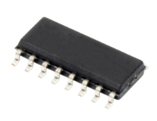
Analog Devices Inc.The ADM2483 differential bus transceiver is an integrated,galvanically isolated component designed for bidirectional datacommunication on balanced, multipoint bus transmission lines.It complies with ANSI EIA/TIA-485-A and ISO 8482: 1987(E).Using the iCoupler technology from Analog Devices, Inc., theADM2483 combines a 3-channel isolator, a three-state differentialline driver, and a differential input receiver into a single package.The logic side of the device is powered with either a 5 V or 3 Vsupply, and the bus side uses a 5 V supply only.The ADM2483 is slew-limited to reduce reflections withimproperly terminated transmission lines. The controlled slewrate limits the data rate to 500 kbps. The device’s input impedanceis 96 kΩ, allowing up to 256 transceivers on the bus. Its driverhas an active-high enable feature. The driver differential outputsand receiver differential inputs are connected internally to forma differential input/output (I/O) port.When the driver is disabled or when VDD1 or VDD2 = 0 V, thisimposes minimal loading on the bus. An active-high receiverdisable feature, which causes the receive output to enter a highimpedance state, is provided as well.The receiver inputs have a true fail-safe feature that ensures alogic-high receiver output level when the inputs are open orshorted. This guarantees that the receiver outputs are in aknown state before communication begins and at the pointwhen communication ends.Current limiting and thermal shutdown features protect againstoutput short circuits and bus contention situations that mightcause excessive power dissipation. The part is fully specifiedover the industrial temperature range and is available in a16-lead, wide body SOIC package.Applications Low power RS-485/RS-422 networks Isolated interfaces Building control networks Multipoint data transmission systems
ADM3076EARZ
Part Number : ADM3076EARZ
Analog Devices Inc.The ADM307xE are 3.3 V, low power data transceivers with ±15 kV ESD protection suitable for full- and half-duplex communication on multipoint bus transmission lines. They are designed for balanced data transmission, and they comply with TIA/EIA standards: RS-485 and RS-422.The devices have a ⅛ unit load receiver input impedance, which allows up to 256 transceivers on a bus. Because only one driver should be enabled at any time, the output of a disabled or powered-down driver is tristated to avoid overloading the bus.The receiver inputs have a true fail-safe feature, which eliminates the need for external bias resistors and ensures a logic high output level when the inputs are open or shorted. This guarantees that the receiver outputs are in a known state before communication begins and when communication ceases.Applications Power/energy metering Industrial control Lighting systems Telecommunications Security systems Instrumentation
ADM3077EARZ
Part Number : ADM3077EARZ
Analog Devices Inc.The ADM307xE are 3.3 V, low power data transceivers with ±15 kV ESD protection suitable for full- and half-duplex communication on multipoint bus transmission lines. They are designed for balanced data transmission, and they comply with TIA/EIA standards: RS-485 and RS-422.The devices have a ⅛ unit load receiver input impedance, which allows up to 256 transceivers on a bus. Because only one driver should be enabled at any time, the output of a disabled or powered-down driver is tristated to avoid overloading the bus.The receiver inputs have a true fail-safe feature, which eliminates the need for external bias resistors and ensures a logic high output level when the inputs are open or shorted. This guarantees that the receiver outputs are in a known state before communication begins and when communication ceases.Applications Power/energy metering Industrial control Lighting systems Telecommunications Security systems Instrumentation
ADM3222ARUZ
Part Number : ADM3222ARUZ
Analog Devices Inc.The ADM3202 / ADM3222 / ADM1385 are high speed, 2-channel RS232/V.28 interface devices which operate from a single +3.3 V power supply. Low power consumption and a shutdown facility (ADM3222 / ADM1385) makes them ideal for battery powered portable instruments.The ADM3202 / ADM3222 / ADM1385 conform to the EIA-232E and CCITT V.28 specifications and operate at data rates up to 230 kbps. Four external 0.1 µF charge pump capacitors are used for the voltage doubler/inverter permitting operation from a single +3.3 V supply.The ADM3222 / ADM1385 contain additional enable and shutdown circuitry. The EN input may be used to three-state the receiver outputs. The SD input is used to power down the charge pump and transmitter outputs reducing the quiescent current to less than 1 µA. The receivers remain enabled during shutdown unless disabled using EN.The ADM3202 is available in a 16-lead DIP, narrow and wide SO as well as a space saving TSSOP package. The ADM3222 is available in 18 lead DIP , SO and in 20 lead SSOP and TSSOP. The ADM1385 is available in a 20 lead SSOP package and is pin compatible with the LTC1385 CG.
ADM3307EACPZ
Part Number : ADM3307EACPZ
Analog Devices Inc.Operating from a single supply as low as +2.7 V, the ADM3307E is a five-driver/three-receiver serial port transceiver, and fully meets full EIA-232 standards. It features an on-board, charge pump dc-to-dc converter, which eliminates the need for dual power supplies. This dc-to-dc converter also contains a voltage tripler and voltage inverter for internally generating positive and negative supplies from the power supply. It operates in Green Idle Mode, where the charge pump oscillator is gated on and off to maintain output voltage to +/-7.25 V, regardless of the load conditions. It has the added benefit of having +15kV ESD protection on both the RS-232 I/O pins and the TTL pins, making it ideal for harsh environments. It also operates at speeds of up to 1Mbps. The ADM3307E is available in a 28-pin TSSOP package as well as a space-saving 32-pin LFCSP package.APPLICATIONS Mobile phone handsets/data cables Laptop and notebook computers Printers Peripherals Modems PDAs/Hand-Held Devices/Palmtop Computers
ADM3312EACPZ
Part Number : ADM3312EACPZ
Analog Devices Inc.The ADM3312E is a three-driver/three-receiver serial port transceiver, which meets full EIA-232 standards while operating from a single power supply as low as +2.7V. It features an on-board, charge pump dc-to-dc converter, which eliminates the need for dual power supplies. This dc-to-dc converter also contains a voltage tripler and voltage inverter for internally generating positive and negative supplies from the power supply. It operates in Green Idle Mode, where the charge pump oscillator is gated on and off to maintain output voltage to +/-7.25 V, regardless of the load conditions. Another key feature is its ESD protection: up to +/-15kV on all I/O lines. The ADM3312E is available in a 24-pin TSSOP package as well as a space-saving 32-pin LFCSP package.APPLICATIONS Mobile phone handsets/data cables Laptop and notebook computers Printers Peripherals Modems PDAs/Hand-Held Devices/Palmtop Computers
ADM696SQ
Part Number : ADM696SQ
Analog Devices Inc.The ADM696 / ADM697 supervisory circuits offer complete single chip solutions for power supply monitoring and battery control functions in microprocessor systems. These functions include µP reset, backup-battery switchover, watchdog timer, CMOS RAM write protection, and power failure warning.The ADM696 / ADM697 are available in 16-pin DIP and small outline packages and provide the following functions: Power-On Reset output during power-up, power-down and brownout conditions. The RESET voltage threshold is adjustable using an external voltage divider. The RESET output remains operational with VCC as low as 1 V. A Reset pulse if the optional watchdog timer has not been toggled within specified time. Separate watchdog time-out and low line status outputs. Adjustable reset and watchdog timeout periods. A 1.3 V threshold detector for power fail warning, low battery detection, or to monitor a power supply other than VCC. Battery backup switching for CMOS RAM, CMOS micro-processor or other low power logic (ADM696). Write protection of CMOS RAM or EEPROM (ADM697).The ADM696 / ADM697 is fabricated using an advanced epitaxial CMOS process combining low power consumption (5 mW), extremely fast Chip Enable gating (5 ns) and high reliability. RESET assertion is guaranteed with VCC as low as 1 V. In addition, the power switching circuitry is designed for minimal voltage drop thereby permitting increased output current drive of up to 100 mA without the need for an external pass transistor.
ADM697ARZ
Part Number : ADM697ARZ
Analog Devices Inc.The ADM696 / ADM697 supervisory circuits offer complete single chip solutions for power supply monitoring and battery control functions in microprocessor systems. These functions include µP reset, backup-battery switchover, watchdog timer, CMOS RAM write protection, and power failure warning.The ADM696 / ADM697 are available in 16-pin DIP and small outline packages and provide the following functions: Power-On Reset output during power-up, power-down and brownout conditions. The RESET voltage threshold is adjustable using an external voltage divider. The RESET output remains operational with VCC as low as 1 V. A Reset pulse if the optional watchdog timer has not been toggled within specified time. Separate watchdog time-out and low line status outputs. Adjustable reset and watchdog timeout periods. A 1.3 V threshold detector for power fail warning, low battery detection, or to monitor a power supply other than VCC. Battery backup switching for CMOS RAM, CMOS micro-processor or other low power logic (ADM696). Write protection of CMOS RAM or EEPROM (ADM697).The ADM696 / ADM697 is fabricated using an advanced epitaxial CMOS process combining low power consumption (5 mW), extremely fast Chip Enable gating (5 ns) and high reliability. RESET assertion is guaranteed with VCC as low as 1 V. In addition, the power switching circuitry is designed for minimal voltage drop thereby permitting increased output current drive of up to 100 mA without the need for an external pass transistor.
ADN2813ACPZ
Part Number : ADN2813ACPZ
Analog Devices Inc.The ADN2813 provides the receiver functions of quantization, signal level detect, and clock and data recovery for continuous data rates from 12.3 Mb/s to 1.25 Gb/s. The ADN2813 automatically locks to all data rates without the need for an external reference clock or programming. All SONET jitter requirements are met, including jitter transfer, jitter generation, and jitter tolerance. All specifications are quoted for −40°C to+85°C ambient temperature, unless otherwise noted.This device, together with a PIN diode and a TIA preamplifier, can implement a highly integrated, low cost, low power fiber optic receiver.The receiver front end loss of signal (LOS) detector circuit indicates when the input signal level has fallen below a useradjustable threshold. The LOS detect circuit has hysteresis to prevent chatter at the output.The ADN2813 is available in a compact 5 mm × 5 mm 32-lead chip scale package.ApplicationsSONET OC-1/3/12 and all associated FEC rates Fibre Channel, GbE, HDTV, etc.WDM transpondersRegenerators/repeatersTest equipmentBroadband cross-connects and routers
ADSP-BF536BBCZ-3B
Part Number : ADSP-BF536BBCZ-3B
Analog Devices Inc.The Blackfin® Processor family has been expanded to address the ever-increasing need for pervasive embedded network connectivity. This connectivity is powerful when utilized in conjunction with the high performance 16-/32-bit Blackfin embedded processor core, the flexible cache architecture, the enhanced DMA subsystem, and the Dynamic Power Management (DPM) functionality. System designers can take advantage of the combined control and signal processing capabilities of the processor core across a wide range of end applications through the scalability of the pin and code compatibility of these new family members. The ADSP-BF536 and ADSP-BF537 are a functional extension of the popular ADSP-BF531 / ADSP-BF532 / ADSP-BF533 processors, and they are ideally suited for a variety of networked applications. The ADSP-BF537 is the higher performance series member, with more embedded memory enabling higher throughput needs for embedded applications suchas video security/surveillance and industrial-environment-based distributed control/factory automation applications. The ADSP-BF536 offers exceptional performance and is designed for low cost connected devices such as remote monitoring devices, VoIP, point-of-sale terminals, and biometrics/security applications. Both devices are ideally suited for a broadrange of industrial, instrumentation, medical, and consumer appliance applications— allowing for scalability based upon the required network bandwidth and mix of control, plus signal processing needed in the end product.
ADUC845BSZ62-5
Part Number : ADUC845BSZ62-5
Analog Devices Inc.The ADuC845, ADuC847, and ADuC848 are single-cycle,12.58 MIPs, 8052 core upgrades to the ADuC834 andADuC836. They include additional analog inputs forapplications requiring more ADC channels.The ADuC845, ADuC847, and ADuC848 are complete smarttransducer front ends. The family integrates high resolutionΣ-Δ ADCs with flexible, up to 10-channel, input multiplexing, afast 8-bit MCU, and program and data Flash/EE memory on asingle chip.The ADuC845 includes two (primary and auxiliary) 24-bit Σ-ΔADCs with internal buffering and PGA on the primary ADC.The ADuC847 includes the same primary ADC as the ADuC845(auxiliary ADC removed). The ADuC848 is a 16-bit ADCversion of the ADuC847.The ADCs incorporate flexible input multiplexing, a temperaturesensor (ADuC845 only), and a PGA (primary ADC only)allowing direct measurement of low-level signals. The ADCsinclude on-chip digital filtering and programmable output datarates that are intended for measuring wide dynamic range andlow frequency signals, such as those in weigh scale, strain gage,pressure transducer, or temperature measurement applications.The devices operate from a 32 kHz crystal with an on-chip PLLgenerating a high frequency clock of 12.58 MHz. This clock isrouted through a programmable clock divider from which theMCU core clock operating frequency is generated. The microcontrollercore is an optimized single-cycle 8052 offering up to12.58 MIPs performance while maintaining 8051 instruction setcompatibility.The available nonvolatile Flash/EE program memory optionsare 62 kbytes, 32 kbytes, and 8 kbytes. 4 kbytes of nonvolatileFlash/EE data memory and 2304 bytes of data RAM are alsoprovided on-chip. The program memory can be configured asdata memory to give up to 60 kbytes of NV data memory indata logging applications.On-chip factory firmware supports in-circuit serial downloadand debug modes (via UART), as well as single-pin emulationmode via the EA pin. The ADuC845, ADuC847, and ADuC848are supported by the QuickStart™ development system featuringlow cost software and hardware development tools.Applications Multichannel sensor monitoring Industrial/environmental instrumentation Weigh scales, pressure sensors, temperature monitoring Portable instrumentation, battery-powered systems Data logging, precision system monitoring
ADV7125BCPZ170
Part Number : ADV7125BCPZ170
Analog Devices Inc.The ADV7125 (ADV®) is a triple high speed, digital-to-analogconverter (DAC) on a single monolithic chip. It consists of threehigh speed, 8-bit video DACs with complementary outputs, astandard TTL input interface, and a high impedance, analogoutput current source.The ADV7125 has three separate 8-bit-wide input ports. Asingle +5 V/+3.3 V power supply and clock are all that arerequired to make the device functional. The ADV7125 hasadditional video control signals, composite SYNC and BLANKas well as a power save mode.The ADV7125 is fabricated in a 5 V CMOS process. Itsmonolithic CMOS construction ensures greater functionalitywith lower power dissipation. The ADV7125 is available in 48-lead LQFP and 48-lead LFCSP packages.Product Highlights 330 MSPS (3.3 V only) throughput. Guaranteed monotonic to eight bits. Compatible with a wide variety of high resolution color graphics systems, including RS-343A and RS-170.Applications Digital video systems High resolution color graphics Digital radio modulation Image processing Instrumentation Video signal reconstruction Automotive infotainment units
ADV7179BCPZ
Part Number : ADV7179BCPZ
Analog Devices Inc.The ADV7179 is suitable for a wide range of video applications such as 3rd generation mobile phones or digital still cameras for video output functionality where package space is as a premium.The ADV7179 comes in a compact chip-scale package, measuring just 6mm by 6mm square, with options for CCIR656 standard video input, with or without embedded timing information.Video performance is not compromised. Advanced filtering (SSAF filters) and professional-level video SNR up to -80dB provides for excellent display quality in a compact format.For more information, download the datasheet today using the links on the left.APPLICATIONS Portable video applications Mobile phones Digital still cameras
DC1053A-H
Part Number : DC1053A-H
Analog Devices Inc.The LTC3526/LTC3526B are synchronous, fixed frequency step-up DC/DC converters with output disconnect. Synchronous rectification enables high efficiency in the low profile 2mm × 2mm DFN package. Battery life in single AA/AAA powered products is extended further with an 850mV start-up voltage and operation down to 500mV once started.A switching frequency of 1MHz minimizes solution footprint by allowing the use of tiny, low profile inductors and ceramic capacitors. The current mode PWM design is internally compensated, reducing external parts count. The LTC3526 features automatic Burst Mode operation at light load conditions, while the LTC3526B features continuous switching at light loads. Anti-ringing control circuitry also reduces EMI concerns by damping the inductor in discontinuous mode. Additional features include a low shutdown current of under 1μA and thermal shutdown.The LTC3526/LTC3526B are housed in a 2mm × 2mm × 0.75mm DFN package.For new designs, we recommend the LTC3526L/LTC3526LB. Startup Voltage Frequency Burst Mode Notes LTC3526 1V 1MHz Yes Not Recommended For New Designs LTC3526B 1V 1MHz No Not Recommended For New Designs LTC3526-2 1V 2MHz Yes Not Recommended For New Designs LTC3526B-2 1V 2MHz No Not Recommended For New Designs LTC3526L 0.85V 1MHz Yes LTC3526LB 0.85V 1MHz No LTC3526L-2 0.85V 2MHz Yes LTC3526LB-2 0.85V 2MHz No APPLICATIONS Medical Instruments Flash-Based MP3 Players Noise Canceling Headphones Wireless Mice Bluetooth Headsets
DC981A/B
Part Number : DC981A/B
Analog Devices Inc.The LTC4263 is an autonomous single-channel PSE controller for use in IEEE 802.3af compliant Power over Ethernet systems. It includes an on-board power MOSFET, internal inrush, current limit, and short-circuit control, IEEE 802.3af compliant PD detection and classification circuitry, and selectable AC or DC disconnect sensing. On-board control algorithms provide complete IEEE 802.3af compliant operation without the need of a microcontroller. The LTC4263 simplifies PSE implementation, needing only a single 48V supply and a small number of passive support components.Programmable on-board power management circuitry permits multiple LTC4263s to allocate and share power in multi-port systems, allowing maximum utilization of the 48V power supply—all without the intervention of a host processor. The port current limit can be configured to automatically adjust to the detected PD class. Detection back-off timing is configurable for either Endpoint or Midspan operation. Built-in foldback and thermal protection provide comprehensive fault protection.An LED pin indicates the state of the port controlled by the LTC4263. When run from a single 48V supply, the LED pin can operate as a simple switching current source to reduce power dissipation in the LED drive circuitry.The LTC4263 is available in 14-pin 4mm × 3mm DFN and 14-pin SO packages.Applications IEEE 802.3af Compliant Endpoint/Midspan PSEs Single-Port or Multi-Port Power Injectors Power Forwarders Low-Port Count PSEs Environment B PSEs Standalone PSEs


