
LTM8046MPY
Part Number : LTM8046MPY
Analog Devices Inc.Switching Voltage Regulators 3.1VIN to 31VIN, 2kVAC Iso DC/DC Modul

AD5337ARMZ
Part Number : AD5337ARMZ
Analog Devices Inc.The AD5337 / AD5338 / AD5339 are dual 8-, 10-, and 12-bit buffered voltage output DACs, respectively. Each part is housed in an 8-lead MSOP package and operates from a single 2.5 V to 5.5 V supply, consuming 250 μA at 3 V. On-chip output amplifiers allow rail-to-rail output swing with a slew rate of 0.7 V/μs. A 2-wire serial interface operates at clock rates up to 400 kHz. This interface is SMBus compatible at VDD < 3.6 V. Multiple devices can be placed on the same bus.The references for the two DACs are derived from one reference pin. The outputs of all DACs can be updated simultaneously using the software LDAC function. The parts incorporate a power-on reset circuit to ensure that the DAC outputs power up to 0 V and remain there until a valid write to the device takes place. A software clear function resets all input and DAC registers to 0 V. A power-down feature reduces the current consumption of the devices to 200 nA @ 5 V (80 nA @ 3 V).The low power consumption of these parts in normal operation makes them ideally suited to portable battery-operated equipment. The power consumption is typically 1.5 mW at 5 V and 0.75 mW at 3 V, reducing to 1 μW in power-down mode.APPLICATIONS Portable battery-powered instruments Digital gain and offset adjustment Programmable voltage and current sources Programmable attenuators Industrial process control

AD5420ACPZ-REEL7
Part Number : AD5420ACPZ-REEL7
Analog Devices Inc.The AD5410/AD5420 are low cost, precision, fully integrated 12-/16-bit converters offering a programmable current source output designed to meet the requirements of industrial process control applications. The output current range is programmable at 4 mA to 20 mA, 0 mA to 20 mA, or an overrange function of 0 mA to 24 mA. The output is open-circuit protected. The device operates with a power supply (AVDD) range from 10.8 V to 60 V. Output loop compliance is 0 V to AVDD − 2.5 V.The flexible serial interface is SPI, MICROWIRE™, QSPI™, and DSP compatible and can be operated in 3-wire mode to minimize the digital isolation required in isolated applications.The device also includes a power-on reset function, ensuring that the device powers up in a known state, and an asynchronous CLEAR pin that sets the output to the low end of the selected current range.The total unadjusted error is typically ±0.01% FSR.Applications Process control Actuator control PLC HART network connectivity

AD5422BCPZ-REEL7
Part Number : AD5422BCPZ-REEL7
Analog Devices Inc.The AD5412/AD5422 are low cost, precision, fully integrated12-/16-bit digital-to-analog converters (DAC) offering a programmable current source and programmable voltage output designed to meet the requirements of industrial process control applications.The output current range is programmable at 4 mA to 20 mA, 0 mA to 20 mA, or an overrange function of 0 mA to 24 mA.The LFCSP version of this product has a CAP2 pin so that the HART signals can be coupled onto the current output of the AD5412/AD5422.Voltage output is provided from a separate pin that can be configured to provide 0 V to 5 V, 0 V to 10 V, ±5 V, or ±10 V output ranges; an overrange of 10% is available on all ranges.Analog outputs are short and open-circuit protected and can drive capacitive loads of 1 μF.The device operates with an AVDD power supply range from 10.8 V to 40 V. Current loop compliance voltage is 0 V to AVDD − 2.5 V.The flexible serial interface is SPI- and MICROWIRE™-compatible and can be operated in 3-wire mode to minimize the digital isolation required in isolated applications.The device also includes a power-on-reset function, ensuring that the device powers up in a known state. The part also includes an asynchronous clear pin (CLEAR) that sets the outputs to zero-scale/midscale voltage output or the low end of the selected current range.The total output error is typically ±0.01% in current mode and ±0.01% in voltage mode.Applications Process controls Actuator controls PLC HART network connectivity (LFCSP package only)

AD549LHZ
Part Number : AD549LHZ
Analog Devices Inc.The AD549 is a monolithic electrometer operational amplifier with very low input bias current. Input offset voltage and input offset voltage drift are laser trimmed for precision performance. The ultralow input current of the part is achieved with Topgate™ JFET technology, a process development exclusive to Analog Devices, Inc. This technology allows fabrication of extremely low input current JFETs compatible with a standard junction isolated bipolar process. The 1015 Ω common-mode impedance, which results from the bootstrapped input stage, ensures that the input current is essentially independent of the common-mode voltage.The AD549 is suited for applications that require very low input current and low input offset voltage. It excels as a preamp for a wide variety of current output transducers, such as photo-diodes, photomultiplier tubes, or oxygen sensors. The AD549 can also be used as a precision integrator or low droop sample and hold. The AD549 is pin compatible with standard FET and electrometer op amps, allowing designers to upgrade the performance of present systems at little additional cost.The AD549 is available in a TO-99 hermetic package. The case is connected to Pin 8 so that the metal case can be independently connected to a point at the same potential as the input terminals, minimizing stray leakage to the case. The AD549 is available in four performance grades. The J, K, and L versions are rated over the commercial temperature range of 0°C to +70°C. The S grade is specified over the military temperature range of −55°C to +125°C and is available processed to MIL-STD-883B, Rev. C. Extended reliability plus screening is also available. Plus screening includes 168 hour burn-in, as well as other environmental and physical tests derived from MIL-STD-883B, Rev. C.Product Highlights The AD549 input currents are specified, 100% tested, and guaranteed after the device is warmed up. They are guaranteed over the entire common-mode input voltage range. The AD549 input offset voltage and drift are laser trimmed to 0.50 mV and 15 μV/°C (AD549K), and to 1 mV and 20 μV/°C (AD549J).. A maximum quiescent supply current of 700 μA minimizes heating effects on input current and offset voltage. AC specifications include 1 MHz unity gain bandwidth and 3 V/μs slew rate. Settling time for a 10 V input step is 5 μs to 0.01%. Applications Electrometer amplifier Photodiode preamp pH electrode buffer

AD5621BKSZ-REEL7
Part Number : AD5621BKSZ-REEL7
Analog Devices Inc.The AD5601/AD5611/AD5621, members of the nanoDAC® family, are single, 8-/10-/12-bit, buffered voltage output DACs that operate from a single 2.7 V to 5.5 V supply, consuming typically 75 μA at 5 V. The parts come in tiny LFCSP and SC70 packages. Their on-chip precision output amplifier allows rail-to-rail output swing to be achieved. The AD5601/AD5611/AD5621 utilize a versatile 3-wire serial interface that operates at clock rates up to 30 MHz and is compatible with SPI, QSPI™, MICROWIRE™, and DSP interface standards.The reference for the AD5601/AD5611/AD5621 is derived from the power supply inputs and, therefore, gives the widest dynamic output range. The parts incorporate a power-on reset circuit, which ensures that the DAC output powers up to 0 V and remains there until a valid write to the device takes place.The AD5601/AD5611/AD5621 contain a power-down feature that reduces current consumption to typically 0.2 μA at 3 V.They also provide software-selectable output loads while in power-down mode. The parts are put into power-down mode over the serial interface.The low power consumption of these parts in normal operation makes them ideally suited to portable battery-operated equip-ment. The combination of small package and low power makes these nanoDAC devices ideal for level-setting requirements, such as generating bias or control voltages in space-constrained and power-sensitive applications.Product Highlights Available in 6-lead LFCSP and SC70 packages. Low power, single-supply operation. The AD5601/ AD5611/AD5621 operate from a single 2.7 V to 5.5 V supply with a maximum current consumption of 100 μA, making them ideal for battery-powered applications. The on-chip output buffer amplifier allows the output of the DAC to swing rail-to-rail with a typical slew rate of 0.5 V/μs. Reference is derived from the power supply. High speed serial interface with clock speeds up to 30 MHz. Designed for very low power consumption. The interface powers up only during a write cycle. Power-down capability. When powered down, the DAC typically consumes 0.2 μA at 3 V. Power-on reset with brownout detection.Applications Voltage level setting Portable battery-powered instruments Digital gain and offset adjustment Programmable voltage and current sources Programmable attenuators

AD5722AREZ
Part Number : AD5722AREZ
Analog Devices Inc.The AD5722/AD5732/AD5752 are dual, 12-/14-/16-bit, serial input, voltage output, digital-to-analog converters. They operate from single-supply voltages from +4.5 V up to +16.5 V or dual-supply voltages from ±4.5 V up to ±16.5 V. Nominal full-scale output range is software-selectable from +5 V, +10 V, +10.8 V, ±5 V, ±10 V, or ±10.8 V. Integrated output amplifiers, reference buffers, and proprietary power-up/power-down control circuitry are also provided.The parts offer guaranteed monotonicity, integral nonlinearity (INL) of ±16 LSB maximum, low noise, and 10 μs typical settling time.The AD5722/AD5732/AD5752 use a serial interface that operates at clock rates up to 30 MHz and are compatible with DSP and microcontroller interface standards. Double buffering allows the simultaneous updating of all DACs. The input coding is user-selectable twos complement or offset binary for a bipolar output (depending on the state of Pin BIN/2sComp), and straight binary for a unipolar output. The asynchronous clear function clears all DAC registers to a user-selectable zero-scale or midscale output. The parts are available in a 24-lead TSSOP and offer guaranteed specifications over the −40°C to +85°C industrial temperature range. The AD5722/AD5732/AD5752 are pin compatible with theAD5724/AD5734/AD5754, which are complete, quad, 12-/14-/ 16-bit, serial input, unipolar/bipolar voltage output DACs.ApplicationsIndustrial automationClosed-loop servo control, process controlAutomotive test and measurementProgrammable logic controllers

AD5724RBREZ-REEL7
Part Number : AD5724RBREZ-REEL7
Analog Devices Inc.The AD5724R/AD5734R/AD5754R are quad, 12-/14-/16-bit serial input, voltage output, digital-to-analog converters(DACs). They operate from single supply voltages of +4.5 V up to +16.5 V or dual supply voltages from ±4.5 V up to ±16.5 V. Nominal full-scale output range is software selectable from +5 V, +10 V, +10.8 V, ±5 V, ±10 V, or ±10.8 V. Integrated output amplifiers, reference buffers, and proprietary power-up/power-down control circuitry are also provided. The devices offer guaranteed monotonicity, integral nonlinearity (INL) of ±16 LSB maximum, low noise, 10 µs typical settling time, and an on-chip +2.5 V reference. The AD5724R/AD5734R/AD5754R use a serial interface that operates at clock rates up to 30 MHz and are compatible with DSP and microcontroller interface standards. Double buffering allows the simultaneous updating of all DACs. The input coding is user-selectable twos complement or offset binary for a bipolar output (depending on the state of Pin BIN/2sCOMP) and straight binary for a unipolar output. The asynchronous clear function clears all DAC registers to a user-selectable zero-scale or midscale output. The devices are available in a 24-lead TSSOP and offer guaranteed specifications over the −40°C to +85°C industrial temperature range.APPLICATIONS Industrial automation Closed-loop servo control, process control Automotive test and measurement Programmable logic controllers Table 1. Pin Compatible Devices Device Number Description AD5724/AD5734/AD5754 AD5724R/AD5734R/AD5754R without internal reference. AD5722/AD5732/AD5752 Complete, dual, 12-/14-/16-bit, serial input, unipolar/bipolar, voltage output DACs. AD5722R/AD5732R/AD5752R AD5722/AD5732/AD5752 with internal reference.

AD582KD
Part Number : AD582KD
Analog Devices Inc.The AD582 is a sample-and-hold amplifier consisting of a high performance operational amplifier, a low leakage analog switch and a JFET integrating amplifier – all fabricated on a single monolithic chip. An external holding capacitor, connected to the device, completes the sample-and-hold function.With the analog switch closed, the AD582 functions like a standard op amp; any feedback network may be connected around the device to control gain and frequency response. With the switch open, the capacitor holds the output at its last level, regardless of input voltage.Typical applications for the AD582 include sampled data systems, D/A deglitchers, analog de-multiplexers, auto null systems, strobed measurement systems and A/D speed enhancement.The device is available in two versions: the 'K' specified for operation over the 0 to +70° commercial temperature range and the 'S' specified over the extended temperature range, -55°C to +125°C. All versions may be obtained in either the hermetic sealed, TO-100 can or the TO-116 DIP.Product HighlightsThe specially designed input stage presents a high impedance to the signal source in both sample and hold modes (up to ±12V). Even with signal levels up to ±VS, no undesirable signal inversion, peaking or loss of hold voltage occurs.The AD582 may be connected in any standard op amp configuration to control gain or frequency response and provide signal inversion, etc.The AD582 offers a high, sample-to-hold current ratio: 107. The ratio of the available charging current to the holding leakage current is often used as a figure of merit for a sample and hold circuit.The AD582 has a typical charge transfer less than 2pC. A low charge transfer produces less offset error and permits the use of smaller hold capacitors for faster signal acquisition.The AD582 provides separate analaog and digital grounds, thus improving the device's immunity to ground and switching transients.The AD582 is available in versions compliant with MIL-STD-883. Refer to the Analog Devices Military Products Databook or current AD582/883B data sheet for detailed specifications.

AD620BNZ
Part Number : AD620BNZ
Analog Devices Inc.The AD620 is a low cost, high accuracy instrumentation amplifier that requires only one external resistor to set gains of 1 to 10,000. Furthermore, the AD620 features 8-lead SOIC and DIP packaging that is smaller than discrete designs and offers lower power (only 1.3 mA max supply current), making it a good fit for battery powered, portable (or remote) applications.The AD620, with its high accuracy of 40 ppm maximum nonlinearity, low offset voltage of 50 µV max, and offset drift of 0.6 µV/°C max, is ideal for use in precision data acquisition systems, such as weigh scales and transducer interfaces. Furthermore, the low noise, low input bias current, and low power of the AD620 make it well suited for medical applications such as ECG and noninvasive blood pressure monitors.The low input bias current of 1.0 nA max is made possible with the use of Superϐeta processing in the input stage. The AD620 works well as a preamplifier due to its low input voltage noise of 9 nV/√Hz at 1 kHz, 0.28 μV p-p in the 0.1 Hz to 10 Hz band, and 0.1 pA/√Hz input current noise. Also, the AD620 is well suited for multiplexed applications with its settling time of 15 μs to 0.01%, and its cost is low enough to enable designs with one in-amp per channel.APPLICATIONSWeigh scalesECG and medical instrumentationTransducer interfaceData acquisition systemsIndustrial process controlsBattery-powered and portable equipment

AD623ARMZ-REEL7
Part Number : AD623ARMZ-REEL7
Analog Devices Inc.The AD623 is an integrated, single- or dual-supply instrumentation amplifier that delivers rail-to-rail output swing using supply voltages from 2.7 V to 12 V. The AD623 offers user flexibility by allowing single gain set resistor programming and by conforming to the 8-lead industry standard pinout configuration. With no external resistor, the AD623 is configured for unity gain (G = 1), and with an external resistor, the AD623 can be programmed for gains of up to 1000.The accuracy of the AD623 is the result of increasing ac common-mode rejection ratio (CMRR) coincident with increasing gain. Line noise harmonics are rejected due to constant CMRR up to 200 Hz. The AD623 has a wide input common-mode range and amplifies signals with common-mode voltages as low as 150 mV below ground. The AD623 maintains optimal performance with dual and single polarity power supplies.Applications Low power medical instrumentation Transducer interfaces Thermocouple amplifiers Industrial process controls Difference amplifiers Low power data acquisition

AD626BNZ
Part Number : AD626BNZ
Analog Devices Inc.The AD626 is a low cost, true single supply differential amplifier designed for amplifying and low-pass filtering small differential voltages from sources having a large common-mode voltage.The AD626 can operate from either a single supply of +2.4 V to +10 V, or dual supplies of ±1.2 V to ±6 V. The input common-mode range of this amplifier is equal to 6 (+VS - 1 V) which provides a +24 V CMR while operating from a +5 V supply. Furthermore, the AD626 features a CMR of 90 dB typ.The amplifier's inputs are protected against continuous overload of up to 50 V, and RFI filters are included in the attenuator network. The output range is +0.03 V to +4.9 V using a +5 V supply. The amplifier provides a preset gain of 10, but gains between 10 to 100 can be easily configured with an external resistor. Furthermore, a gain of 100 is available by connecting the G = 100 pin to analog ground. The AD626 also offers low-pass filter capability by connecting a capacitor between the filter pin and analog ground.The AD626A and AD626B operate over the industrial temperature range of -40°C to +85°C. The AD626 is available in two 8-pin packages: a plastic mini-DIP and SOIC.

AD628ARMZ
Part Number : AD628ARMZ
Analog Devices Inc.The AD628 is a precision difference amplifier that combines excellent dc performance with high common-mode rejection over a wide range of frequencies. When used to scale high voltages, it allows simple conversion of standard control voltages or currents for use with single-supply ADCs. A wideband feedback loop minimizes distortion effects due to capacitor charging of Σ-Δ ADCs.A reference pin (VREF) provides a dc offset for converting bipolar to single-sided signals. The AD628 converts +5 V, +10 V, ±5 V, ±10 V, and 4 to 20 mA input signals to a single-ended output within the input range of single-supply ADCs.The AD628 has an input common mode and differential mode operating range of ±120 V. The high common mode, input impedance makes the device well suited for high voltage measurements across a shunt resistor. The inverting input of the buffer amplifier is available for making a remote Kelvin connection.A precision 10 kΩ resistor connected to an external pin is provided for either a low-pass filter or to attenuate large differential input signals. A single capacitor implements a low-pass filter. The AD628 operates from single and dual supplies and is available in an 8-lead SOIC_N or an 8-lead MSOP. It operates over the standard industrial temperature range of −40°C to +85°C.Applications High voltage current shunt sensing Programmable logic controllers Analog input front end signal conditioning +5 V, +10 V, ±5 V, ±10 V, and 4 to 20 mA Isolation Sensor signal conditioning Power supply monitoring Electrohydraulic controls Motor controls

AD629BRZ-R7
Part Number : AD629BRZ-R7
Analog Devices Inc.The AD629 is a difference amplifier with a very high input, common-mode voltage range. It is a precision device that allows the user to accurately measure differential signals in the presence of high common-mode voltages up to ±270 V. The AD629 can replace costly isolation amplifiers in applications that do not require galvanic isolation. The device operates over a ±270 V common-mode voltage range and has inputs that are protected from common-mode or differential mode transients up to ±500 V.The AD629 has low offset, low offset drift, low gain error drift, low common-mode rejection drift, and excellent CMRR over a wide frequency range.The AD629 is available in low cost, 8-lead PDIP and 8-lead SOIC packages. For all packages (including die) and grades, performance is guaranteed over the industrial temperature range of −40°C to +85°C.Applications High voltage current sensing Battery cell voltage monitors Power supply current monitors Motor controls Isolation

AD7147ACPZ-1500RL7
Part Number : AD7147ACPZ-1500RL7
Analog Devices Inc.The AD7147 CapTouch™ controller is designed for use with capacitance sensors implementing functions such as buttons, scroll bars, and wheels. The sensors need only one PCB layer, enabling ultrathin applications.The AD7147 is an integrated CDC with on-chip environmental calibration. The CDC has 13 inputs channeled through a switch matrix to a 16-bit, 250 kHz sigma-delta (Σ-Δ) converter. The CDC is capable of sensing changes in the capacitance of the external sensors and uses this information to register a sensor activation. By programming the registers, the user has full control over the CDC setup.High resolution sensors require minor software to run on the host processor.The AD7147 is designed for single electrode capacitance sensors (grounded sensors). There is an active shield output to minimize noise pickup in the sensor.The AD7147 has on-chip calibration logic to compensate for changes in the ambient environment. The calibration sequence is performed automatically and at continuous intervals as long as the sensors are not touched. This ensures that there are no false or non-registering touches on the external sensors due to a changing environment.The AD7147 has an SPI-compatible serial interface, and the AD7147-1 has an I2C®-compatible serial interface. Both parts have an interrupt output, as well as a GPIO. There is a VDRIVE pin to set the voltage level for the serial interface independent of VCC.The AD7147 is available in a 24-lead, 4 mm × 4 mm LFCSP and operates from a 2.6 V to 3.6 V supply. The operating current consumption in low power mode is typically 26 μA for 13 sensors.APPLICATIONS Cell phones Personal music and multimedia players Smart handheld devices Television, A/V, and remote controls Gaming consoles Digital still cameras

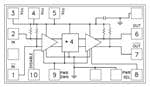
AD7262BSTZ
Part Number : AD7262BSTZ
Analog Devices Inc.The AD7262/AD7262-5 are dual, 12-bit, high speed, low power, successive approximation ADCs that operate from a single 5 V power supply. The AD7262 features throughput rates of up to 1 MSPS per on-chip ADC. The AD7262-5 features throughput rates of up to 500 kSPS. Two complete ADC functions allow simultaneous sampling and conversion of two channels. Each ADC is preceded by a true differential analog input with a PGA. There are 14 gain settings available: ×1, ×2, ×3, ×4, ×6, ×8, ×12, ×16, ×24, ×32, ×48, ×64, ×96, and ×128.The AD7262/AD7262-5 contain four comparators. Comparator A and Comparator B are optimized for low power, while Comparator C and Comparator D have fast propagation delays. The AD7262/AD7262-5 feature a calibration function to remove any device offset error and programmable gain adjust registers to allow for input path (for example, sensor) offset and gain compensation. The AD7262/AD7262-5 have an on-chip 2.5 V reference that can be disabled if an external reference is preferred.The AD7262/AD7262-5 are ideally suited for monitoring small amplitude signals from a variety of sensors. They include all the functionality needed for monitoring the position feedback signals from a variety of analog encoders used in motor control systems.Product Highlights Integrated PGA with a variety of flexible gain settings to allow detection and conversion of low level analog signals. Each PGA is followed by a dual simultaneous sampling ADC, featuring throughput rates of 1 MSPS per ADC for the AD7262. The conversion results of both ADCs are simultaneously available on separate data lines or in succession on one data line if only one serial port is available. Four integrated comparators that can be used to count signals from pole sensors in motor control applications. Internal 2.5 V reference.

AD7367BRUZ-5
Part Number : AD7367BRUZ-5
Analog Devices Inc.The AD7366-5 / AD7367-5 are dual, 12-/14-bit, low power, successive approximation analog-to-digital converters (ADCs) that feature throughput rates up to 500 kSPS. Each device contains two ADCs, which are both preceded by a 2-channel multiplexer, and a low noise, wide bandwidth, track-and-hold amplifier.The AD7366-5 / AD7367-5 are fabricated on the Analog Devices, Inc., industrial CMOS process (iCMOS®), which is a technology platform combining the advantages of low and high voltage CMOS. The process allows the parts to accept high voltage bipolar signals in addition to reducing power consumption and package size. The AD7366-5 / AD7367-5 can accept true bipolar analog input signals in the ±10 V range, ±5 V range, and 0 V to +10 V range.The devices have an on-chip 2.5 V reference that can be disabled to allow the use of an external reference. If a 3 V reference is applied to the DCAPA and DCAPB pins, the AD7366-5 / AD7367-5 can accept a true bipolar ±12 V analog input. Minimum ±12 V VDD and VSS supplies are required for the ±12 V input range.PRODUCT HIGHLIGHTS True bipolar analog input signals can be accepted, as well as ±10 V, ±5 V, ±12 V (with external reference), and 0 V to +10 V unipolar signals. Two complete ADC functions allow simultaneous sampling and conversion of two channels. A 500 kSPS serial interface is SPI-/QSPI™-/MICROWIRE™-/ DSP-compatible.
AD7367BRUZ-5-RL7
Part Number : AD7367BRUZ-5-RL7
Analog Devices Inc.The AD7366-5 / AD7367-5 are dual, 12-/14-bit, low power, successive approximation analog-to-digital converters (ADCs) that feature throughput rates up to 500 kSPS. Each device contains two ADCs, which are both preceded by a 2-channel multiplexer, and a low noise, wide bandwidth, track-and-hold amplifier.The AD7366-5 / AD7367-5 are fabricated on the Analog Devices, Inc., industrial CMOS process (iCMOS®), which is a technology platform combining the advantages of low and high voltage CMOS. The process allows the parts to accept high voltage bipolar signals in addition to reducing power consumption and package size. The AD7366-5 / AD7367-5 can accept true bipolar analog input signals in the ±10 V range, ±5 V range, and 0 V to +10 V range.The devices have an on-chip 2.5 V reference that can be disabled to allow the use of an external reference. If a 3 V reference is applied to the DCAPA and DCAPB pins, the AD7366-5 / AD7367-5 can accept a true bipolar ±12 V analog input. Minimum ±12 V VDD and VSS supplies are required for the ±12 V input range.PRODUCT HIGHLIGHTS True bipolar analog input signals can be accepted, as well as ±10 V, ±5 V, ±12 V (with external reference), and 0 V to +10 V unipolar signals. Two complete ADC functions allow simultaneous sampling and conversion of two channels. A 500 kSPS serial interface is SPI-/QSPI™-/MICROWIRE™-/ DSP-compatible.


