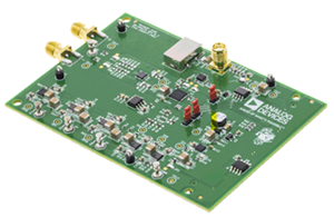
ADL5304-EVALZ
Part Number : ADL5304-EVALZ
Analog Devices Inc.The ADL5304 is a high speed logarithmic converter with fast response and low noise over a 200 dB (1 pA to 10 mA) measurement range. The ADL5304 provides a nominal logarithmic slope of 10 mV/dB (200 mV/decade); other values are easily configured. Logarithmic intercept can be programmed over a wide range with the internal 100 nA current source or externally for log ratio applications.The default intercept value of 3.162 fA places the midpoint of the measurement range of 100 nA at VLOG = 1.5 V.A single positive supply of 5 V is all that is required for operation over a specified 1 pA to 3 mA input range. Dual-supply operation extends the specified input current range to 10 mA.The ADL5304 accepts two current inputs to the logarithmic argument. The numerator input, INUM, flows in the collector of an NPN transistor, connected in a feedback path around a low offset JFET amplifier. The denominator current, IDEN, is treated in the same way, which allows for log ratio operation. The input summing nodes (INUM and IDEN) operate at a constant default voltage of 1.5 V. The VSM1 to VSM4 pins flank the INUM and IDEN inputs to provide a guard voltage to minimize leakage currents.Adaptive photodiode biasing is provided for optical measurements. A monitor current 1.1 times INUM is output at the IMON pin, and an external resistor, RMNTR, at 10 times the photodiode series resistance (RS) applies a voltage across the photodiode that 1st order keeps the internal PD junction at 0 V to minimize dark current.The VLOG output is buffered and can be rescaled through internal gain setting resistors. The internal ILOG varies from −400 μA to +400 μA as INUM changes over 10 decades from 1 pA to 10 mA. This corresponds to 0.5 V to 2.5 V at the VLOG pin in the default configuration shown in Figure 1.Accurate 1.5 V (Pin 1P5V) and 2.0 V (Pin 2VLT) reference outputs allow precise repositioning of the intercept using external resistors.The ADL5304 is available in a 32-lead, 5 mm × 5 mm LFCSP and specified for operation from −40°C to +85°C.Applications High accuracy optical power measurement Wide range baseband log compression Versatile detector for high speed APC loops
ADL5505ACBZ-P7
Part Number : ADL5505ACBZ-P7
Analog Devices Inc.The ADL5505 is a TruPwr™ mean-responding (true rms) powerdetector for use in high frequency receiver and transmitter signalchains from 450 MHz to 6000 MHz. Requiring only a singlesupply between 2.5 V and 3.3 V, the detector draws less than1.8 mA. The input is internally ac-coupled and has a nominalinput impedance of 500 Ω. The rms output is a linear-respondingdc voltage with a conversion gain of 1.86 V/V rms at 900 MHz.The ADL5505 is a highly accurate, easy to use means ofdetermining the rms of complex waveforms. It can be used forpower measurements of both simple and complex waveformsbut is particularly useful for measuring high crest factor (highpeak-to-rms ratio) signals, such as W-CDMA, CDMA2000,WiMAX, WLAN, and LTE waveforms.The on-chip modulation filter provides adequate averaging formost waveforms. An on-chip, 100 Ω series resistance at theoutput, combined with an external shunt capacitor, creates a low-passfilter response that reduces the residual ripple in the dc outputvoltage.The ADL5505 offers excellent temperature stability across a30 dB range and near 0 dB measurement error across temperatureover the top portion of the dynamic range. In addition to itstemperature stability, the ADL5505 offers low process variationsthat further reduce calibration complexity.The power detector operates from −40°C to +85°C and isavailable in an 4-ball, 0.8 mm × 0.8 mm wafer-level chip scalepackage. It is fabricated on a high fT silicon BiCMOS process.Applications Power measurement of W-CDMA, CDMA2000, QPSK-/QAM-based OFDM (LTE and WiMAX), and other complex modulation waveforms RF transmitter or receiver power measurement
ADL5536ARKZ-R7
Part Number : ADL5536ARKZ-R7
Analog Devices Inc.The ADL5536 is a 20 dB linear amplifier that operates atfrequencies up to 1 GHz. The device can be used in a widevariety of cellular, CATV, military, and instrumentationequipment.The ADL5536 provides the highest dynamic range availablefrom an internally matched IF gain block. This is accomplishedby providing extremely low noise figures and very high OIP3specifications simultaneously across the entire 1 GHz frequencyrange. The ADL5536 also provides extremely flat gain and P1dBover frequency, which are stable over temperature, power supply,and from device to device.The device is internally matched to 50 Ω at the input and output,making the ADL5536 very easy to implement in a wide varietyof applications. Only input/output ac coupling capacitors, powersupply decoupling capacitors, and an external inductor arerequired for operation.The ADL5536 is fabricated on a GaAs HBT process and has anESD rating of ±2 kV (Class 2). The device is assembled in anMSL-1 rated SOT-89 package that uses an exposed paddle forexcellent thermal impedance.The ADL5536 consumes only 105 mA on a single 5 V supplyand is fully specified for operation from −40°C to +85°C.The ADL5536 is also pin-compatible with the 16 dB gainADL5535. Fully populated evaluation boards are availablefor each amplifier.
ADRF6801ACPZ-R7
Part Number : ADRF6801ACPZ-R7
Analog Devices Inc.The ADRF6801 is a high dynamic range IQ demodulator with integrated PLL and VCO. The fractional-N PLL/synthesizer generates a frequency in the range of 3.0 GHz to 4.6 GHz. A divide-by-4 quadrature divider divides the output frequency of the VCO down to the required local oscillator (LO) frequency to drive the mixers in quadrature. Additionally, an output buffer can be enabled that generates an fVCO/2 signal for external use.The PLL reference input is supported from 10 MHz to 160 MHz. The phase detector output controls a charge pump whose output is integrated in an off-chip loop filter. The loop filter output is then applied to an integrated VCO. The IQ demodulator mixes the differential RF input with the complex LO derived from the quadrature divider. The differential I and Q output paths have excellent quadrature accuracy and can handle baseband signaling or complex IF up to 120 MHz.The ADRF6801 is fabricated using an advanced silicon-germanium BiCMOS process. It is available in a 40-lead, exposed-paddle, RoHS-compliant, 6 mm × 6 mm LFCSP package. Performance is specified over the −40°C to +85°C temperature range.APPLICATIONS QAM/QPSK RF/IF demodulators Cellular W-CDMA/CDMA/CDMA2000 Microwave point-to-(multi)point radios Broadband wireless and WiMAX
ADSP-21478KBCZ-1A
Part Number : ADSP-21478KBCZ-1A
Analog Devices Inc.The fourth generation of SHARC® Processors now includes the low power floating point DSP products – the ADSP-21478 and ADSP-21479 and offers increased performance, hardware-based filter accelerators, audio and application-focused peripherals, and new memory configurations capable of supporting a single chip solution. All devices are pin-compatible with each other and completely code-compatible with all prior SHARC Processors. These newest members of the fourth generation SHARC Processor family are based on a single-instruction, multiple-data (SIMD) core, which supports both 32-bit fixed-point and 32-/40-bit floating-point arithmetic formats and their low power make them particularly suitable for battery powered applications or where a higher ambient operating temperature is required.The ADSP-21478 offers a very low power and high performance – 266 MHz/1596 MFLOPs – in a BGA and LQFP package within the fourth generation SHARC Processor family. This feature of power makes the ADSP-21478 particularly well suited to address the automotive audio and many industrial control segments where low power is a requirement. In addition to its high core performance, the ADSP-21478 includes additional processing blocks such as FIR, IIR, and FFT accelerators to increase the total performance of the system. There is a new feature called Variable Instruction Set Architecture (VISA) that allows the code size to be decreased by 20% to 30% and increase the memory size availability. The fourth generation DSP allows the ability to connect to external memory by providing a glueless interface to 16-bit wide SDR SDRAMs.Fourth-generation SHARC Processors also integrate application-specific peripherals designed to simplify hardware design, minimize design risks, and ultimately reduce time to market. Grouped together, and broadly named the Digital Applications Interface (DAI), these functional blocks may be connected to each other or to external pins via the software-programmable Signal Routing Unit (SRU). The SRU is an innovative architectural feature that enables complete and flexible routing amongst DAI blocks. Peripherals connected through the SRU include but are not limited to serial ports, SPI ports, S/PDIF Tx/Rx, and an 8-Channel asynchronous sample rate converter block. The fourth generation SHARC allows data from the serial ports to be directly transferred to external memory by the DMA controller. Other peripherals such as UART and Two-Wire Interface are routed through a Digital Peripheral Interface (DPI).
ADSP-BF592BCPZ
Part Number : ADSP-BF592BCPZ
Analog Devices Inc.The BF592 is the low cost entry point into the Blackfin portfolio of processors. With core clock speeds of 200 and 400 MHz and a peripheral set including two SPORT’s, a PPI, two SPI’s, four general purpose counters and a factory-programmed Instruction ROM block containing the VDK RTOS and C-runtime libraries, the BF592 is feature and cost optimized for compute intensive industrial, automotive, and general purpose applications that do not require external memory or executable flash. The BF592 is offered in a low cost 9×9mm LFCSP package in commercial and industrial temperature grades as well as automotive qualified.
ADUM4400CRWZ
Part Number : ADUM4400CRWZ
Analog Devices Inc.The ADuM440x are 4-channel digital isolators based on the Analog Devices, Inc., iCoupler® technology. Combining high speed CMOS and monolithic air core transformer technology, these isolation components provide outstanding performance characteristics that are superior to the alternatives, such as optocoupler devices and other integrated couplers.The ADuM440x isolators provide four independent isolation channels in a variety of channel configurations and data rates (see the Ordering Guide). All models operate with the supply voltage on either side ranging from 3.0 V to 5.5 V, providing compatibility with lower voltage systems as well as enabling a voltage translation functionality across the isolation barrier. The ADuM440x isolators have a patented refresh feature that ensures dc correctness in the absence of input logic transitions and during power-up/power-down conditions.This family of isolators, like many Analog Devices isolators, offers very low power consumption, consuming one-tenth to one-sixth the power of comparable isolators at comparable data rates up to 10 Mbps. All models of the ADuM440x provide low pulse width distortion (
ADUM6200ARWZ
Part Number : ADUM6200ARWZ
Analog Devices Inc.The ADuM6200 / ADuM6201 / ADuM6202 are dual-channel digital isolators with isoPower®, an integrated, isolated DC/DC converter. Based on the Analog Devices, Inc., iCoupler® technology, the DC/DC converter provides up to 400 mW of regulated, isolated power at either 5.0 V or 3.3 V from a 5.0 V input supply, or at 3.3 V from a 3.3 V supply at the power levels shown in Table 1 on the data sheet. These devices eliminate the need for a separate, isolated DC/DC converter in low power, isolated designs. The iCoupler chip scale transformer technology is used to isolate the logic signals and for the magnetic components of the DC/DC converter. The result is a small form factor, total isolation solution.The ADuM6200 / ADuM6201 / ADuM6202 isolators provide two independent isolation channels in a variety of channel configurations and data rates (see the Ordering Guide for more information).isoPower uses high frequency switching elements to transfer power through its transformer. Special care must be taken during printed circuit board (PCB) layout to meet emissions standards. See the AN-0971 Application Note for board layout recommendations.APPLICATIONS RS-232/RS-422/RS-485 transceivers Industrial field bus isolation Power supply start-up bias and gate drives Isolated sensor interfaces Industrial PLCs
ADUM6400ARIZ
Part Number : ADUM6400ARIZ
Analog Devices Inc.The ADuM640x devices are quad-channel digital isolators with isoPower®, an integrated, isolated DC/DC converter. Based on the Analog Devices, Inc., iCoupler® technology, the DC/DC converter provides up to 500 mW of regulated, isolated power at either 5.0 V or 3.3 V from a 5.0 V input supply, or 3.3 V from a 3.3 V supply at the power levels shown in Table 1. This eliminates the need for a separate, isolated DC/DC converter in low power, isolated designs. The iCoupler chip scale transformer technology is used to isolate the logic signals and for the magnetic components of the DC/DC converter. The result is a small form factor, total isolation solution.The ADuM640x isolators provide four independent isolation channels in a variety of channel configurations and data rates (see the Ordering Guide for more information).isoPower uses high frequency switching elements to transfer power through its transformer. Special care must be taken during printed circuit board (PCB) layout to meet emissions standards. Refer to the AN-0971 application note for board layout recommendations at www.analog.com.
AD5590BBCZ
Part Number : AD5590BBCZ
Analog Devices Inc.The AD5590 is a 16-channel input and 16-channel output analog I/O port with eight uncommitted amplifiers, operating from a single 4.5 V to 5.25 V supply. The AD5590 comprises 16 input channels multiplexed into a 1 MSPS, 12-bit successive approximation ADC with a sequencer to allow a preprogrammed selection of channels to be converted sequentially. The ADC contains a low noise, wide bandwidth track-and-hold amplifier that can handle input frequencies in excess of 1 MHz.The conversion process and data acquisition are controlled using ASYNC and the serial clock signal, allowing the device to easily interface with microprocessors or DSPs. The input signal is sampled on the falling edge of ASYNC and conversion is also initiated at this point. There are no pipeline delays associated with the ADC. By setting the relevant bits in the control register, the analog input range for the ADC can be selected to be a 0 V to VREFA input or a 0 V to 2 × VREFA with either straight binary or twos complement output coding. The conversion time is determined by the ASCLK frequency because it is also used as the master clock to control the conversion.The DAC section of the AD5590 comprises sixteen 12-bit DACs divided into two groups of eight. Each group has an on-chip reference. The on-board references are off at power-up, allowing the use of external references. The internal references are enabled via a software write.The AD5590 incorporates a power-on reset circuit that ensures that the DAC outputs power up to 0 V and remain powered up at this level until a valid write takes place. The DAC contains a power-down feature that reduces the current consumption of the device and provides software-selectable output loads while in power-down mode for any or all DAC channels. The outputs of all DACs can be updated simultaneously using the LDAC function, with the added functionality of user-selectable DAC channels to simultaneously update. There is also an asynchronous CLR that updates all DACs to a user-programmable code: zero scale, midscale, or full scale.The AD5590 contains eight low noise, single-supply amplifiers. These amplifiers can be used for signal conditioning for the ADCs, DACs, or other independent circuitry, if required.APPLICATIONS Optical Line Cards (Monitoring and Control) Base Stations General Purpose Analog I/O Monitoring and control
AD7190BRUZ
Part Number : AD7190BRUZ
Analog Devices Inc.The AD7190 is a low noise, complete analog front end for high precision measurement applications. It contains a low noise, 24-bit sigma-delta (Σ-Δ) analog-to-digital converter (ADC). The on-chip low noise gain stage means that signals of small amplitude can be interfaced directly to the ADC.The device can be configured to have two differential inputs or four pseudo differential inputs. The on-chip channel sequencer allows several channels to be enabled, and the AD7190 sequentially converts on each enabled channel. This simplifies communication with the part. The on-chip 4.92 MHz clock can be used as the clock source to the ADC or, alternatively, an external clock or crystal can be used. The output data rate from the part can be varied from 4.7 Hz to 4.8 kHz.The device has two digital filter options. The choice of filter affects the rms noise/noise-free resolution at the programmed output data rate, the settling time, and the 50 Hz/60 Hz rejection. For applications that require all conversions to be settled, the AD7190 includes a zero latency feature.The part operates with 5 V analog power supply and a digital power supply from 2.7 V to 5.25 V. It consumes a current of 6 mA. It is housed in a 24-lead TSSOP package.APPLICATIONS Weigh scales Strain gauge transducers Pressure measurement Temperature measurement Chromatography PLC/DCS analog input modules Data acquisition Medical and scientific instrumentation
AD8210YRZ
Part Number : AD8210YRZ
Analog Devices Inc.The AD8210 is a single-supply, difference amplifier ideal for amplifying small differential voltages in the presence of large common-mode voltages. The operating input common-mode voltage range extends from −2 V to +65 V. The typical supply voltage is 5 V. The AD8210 is offered in a SOIC package. The operating temperature range is −40°C to +125°C.Excellent ac and dc performance over temperature keep errors in the measurement loop to a minimum. Offset drift and gain drift are guaranteed to a maximum of 8 μV/°C and 20 ppm/°C, respectively.The output offset can be adjusted from 0.05 V to 4.9 V with a 5 V supply by using the VREF1 pin and the VREF2 pin. With the VREF1 pin attached to the V+ pin and the VREF2 pin attached to the GND pin, the output is set at half scale. Attaching both VREF1 and VREF2 to GND causes the output to be unipolar, starting near ground. Attaching both VREF1 and VREF2 to V+ causes the output to be unipolar, starting near V+. Other offsets can be obtained by applying an external voltage to VREF1 and VREF2.Applications Current sensing Motor controls Transmission controls Diesel injection controls Engine management Suspension controls Vehicle dynamic controls DC-to-dc converters
AD8221ARMZ
Part Number : AD8221ARMZ
Analog Devices Inc.The AD8221 is a gain programmable, high performance instrumentation amplifier that delivers the industry’s highest CMRR over frequency in its class. The CMRR of instrumentation amplifiers on the market today falls off at 200 Hz. In contrast, the AD8221 maintains a minimum CMRR of 80 dB to 10 kHz for all grades at G = 1. High CMRR over frequency allows the AD8221 to reject wideband interference and line harmonics, greatly simplifying filter requirements. Possible applications include precision data acquisition, biomedical analysis, and aerospace instrumentation. Low voltage offset, low offset drift, low gain drift, high gain accuracy, and high CMRR make this part an excellent choice in applications that demand the best dc performance possible, such as bridge signal conditioning. Programmable gain affords the user design flexibility. A single resistor sets the gain from 1 to 1000. The AD8221 operates on both single and dual supplies and is well suited for applications where ±10 V input voltages are encountered. The AD8221 is available in a low cost 8-lead SOIC and 8-lead MSOP, both of which offer the industry’s best performance. The MSOP requires half the board space of the SOIC, making it ideal for multichannel or space-constrained applications. Performance is specified over the entire industrial temperature range of −40°C to +85°C for all grades. Furthermore, the AD8221 is operational from −40°C to +125°C*. ApplicationsWeigh scales Industrial process controls Bridge amplifiers Precision data acquisition systems Medical instrumentation Strain gages Transducer interfaces
AD8224BCPZ-R7
Part Number : AD8224BCPZ-R7
Analog Devices Inc.The AD8224 is the first single-supply, JFET input instrumentation amplifier available in the space-saving 16-lead, 4 mm × 4 mm LFCSP. It requires the same board area as a typical single instrumentation amplifier yet doubles the channel density and offers a lower cost per channel without compromising performance.Designed to meet the needs of high performance, portable instrumentation, the AD8224 has a minimum common-mode rejection ratio (CMRR) of 86 dB at dc and a minimum CMRR of 80 dB at 10 kHz for G = 1. Maximum input bias current is 10 pA and typically remains below 300 pA over the entire industrial temperature range. Despite the JFET inputs, the AD8224 typically has a noise corner of only 10 Hz.With the proliferation of mixed-signal processing, the number of power supplies required in each system has grown.Designed to alleviate this problem, the AD8224 can operate on a ±18 V dual supply, as well as on a single +5 V supply. The device’s rail-to-rail output stage maximizes dynamic range on the low voltage supplies common in portable applications. Its ability to run on a single 5 V supply eliminates the need for higher voltage, dual supplies. The AD8224 draws 750 μA of quiescent current per amplifier, making it ideal for battery powered devices.In addition, the AD8224 can be configured as a single-channel, differential output, instrumentation amplifier. Differential outputs provide high noise immunity, which can be useful when the output signal must travel through a noisy environment, such as with remote sensors. The configuration can also be used to drive differential input ADCs.For a single-channel version, use the AD8220.Applications Medical instrumentation Precision data acquisition Transducer interfaces Differential drives for high resolution input ADCs Remote sensors
AD8226BRZ
Part Number : AD8226BRZ
Analog Devices Inc.The AD8226 is a low cost, wide supply range instrumentation amplifier that requires only one external resistor to set any gain between 1 and 1000.The AD8226 is designed to work with a variety of signal voltages. A wide input range and rail-to-rail output allow the signal to make full use of the supply rails. Because the input range also includes the ability to go below the negative supply, small signals near ground can be amplified without requiring dual supplies. The AD8226 operates on supplies ranging from ±1.35 V to ±18 V for dual supplies and 2.2 V to 36 V for single supply.The robust AD8226 inputs are designed to connect to real-world sensors. In addition to its wide operating range, the AD8226 can handle voltages beyond the rails. For example, with a ±5 V supply, the part is guaranteed to withstand ±35 V at the input with no damage. Minimum as well as maximum input bias currents are specified to facilitate open wire detection.The AD8226 is perfect for multichannel, space-constrained industrial applications. Unlike other low cost, low power instrumentation amplifiers, the AD8226 is designed with a minimum gain of 1 and can easily handle ±10 V signals. With its MSOP package and 125°C temperature rating, the AD8226 thrives in tightly packed, zero airflow designs.The AD8226 is available in 8-lead MSOP and SOIC packages, and is fully specified for −40°C to +125°C operation.For a device with a similar package and performance as the AD8226 but with gain settable from 5 to 1000, consider using the AD8227.ApplicationsIndustrial process controlsBridge amplifiersMedical instrumentationPortable data acquisitionMultichannel systems
AD8622ARZ
Part Number : AD8622ARZ
Analog Devices Inc.The AD8622 is a dual, precision rail-to-rail output operational amplifier with a low supply current of only 350 μA maximum over temperature and supply voltages. It also offers ultralow offset, drift, and voltage noise combined with very low input bias current over the full operating temperature range.With typical offset voltage of only 10 μV, offset drift of 0.5 μV/°C, and noise of only 0.2 μV p-p (0.1 Hz to 10 Hz), it is perfectly suited for applications where large error sources cannot be tolerated. Many systems can take advantage of the low noise, dc precision, and rail-to-rail output swing provided by the AD8622 to maximize the signal-to-noise ratio and dynamic range for low power operation. The AD8622 is specified for the extended industrial temperature range of −40°C to +125°C and is available in lead-free SOIC and MSOP packages.ApplicationsPortable precision instrumentationLaser diode control loopsMedical InstrumentationStrain gage amplifiersThermocouple amplifiers
AD8665ARZ-REEL
Part Number : AD8665ARZ-REEL
Analog Devices Inc.The AD866x family are single supply, rail-to-rail output amplifiers with low noise performance featuring an extended operating range with supply voltages up to 16 V. They also feature low input bias currents, wide signal bandwidth, and low input voltage and current noise. For lower offset voltage, choose the AD8661/AD8662/AD8664 family.The combination of low offset, very low input bias current, and a wide supply range makes these amplifiers useful in a wide variety of applications usually associated with higher priced JFET amplifiers. Systems using high impedance sensors, such as photodiodes, benefit from the combination of low input bias current, low noise, low offset, and wide bandwidth. The wide operating voltage range matches high performance ADCs and DACs. Audio applications and medical monitoring equipment can take advantage of the high input impedance, low voltage and current noise, wide bandwidth, and the lack of popcorn noise found in many other low input bias current amplifiers.The AD866x family is specified over the extended industrial temperature range (−40°C to +125°C). ApplicationsReference Buffers Medical Equipment Physiological measurementsSignal filters and conditioning Consumer audio Photodiode amplificationADC driver Level shifting circuits Data Sheet, Rev. A, 10/06
AD9219ABCPZ-65
Part Number : AD9219ABCPZ-65
Analog Devices Inc.The AD9219 is a quad, 10-bit, 40/65 MSPS analog-to-digital con-verter (ADC) with an on-chip sample-and-hold circuit designedfor low cost, low power, small size, and ease of use. The productoperates at a conversion rate of up to 65 MSPS and is optimized foroutstanding dynamic performance and low power in applications where a small package size is critical.The ADC requires a single 1.8 V power supply and LVPECL-/ CMOS-/LVDS-compatible sample rate clock for full performanceoperation. No external reference or driver components arerequired for many applications.The ADC automatically multiplies the sample rate clock for theappropriate LVDS serial data rate. A data clock output (DCO) for capturing data on the output and a frame clock output (FCO) for signaling a new output byte are provided. Individual-channel power-down is supported and typically consumes less than 2 mW when all channels are disabled.The ADC contains several features designed to maximizeflexibility and minimize system cost, such as programmableclock and data alignment and programmable digital test patterngeneration. The available digital test patterns include built-in deterministic and pseudorandom patterns, along with custom user- defined test patterns entered via the serial port interface (SPI).The AD9219 is available in an RoHS compliant, 48-lead LFCSP. It is specified over the industrial temperature range of −40°C to +85°C.Product Highlights Small Footprint. Four ADCs are contained in a small, space-saving package. Low power of 94 mW/channel at 65 MSPS. Ease of Use. A data clock output (DCO) is provided that operates at frequencies of up to 390 MHz and supports double data rate (DDR) operation. User Flexibility. The SPI control offers a wide range of flexible features to meet specific system requirements. Pin-Compatible Family. This includes the AD9287 (8-bit), AD9228 (12-bit), and AD9259 (14-bit). ApplicationsMedical imaging and nondestructive ultrasoundPortable ultrasound and digital beam-forming systemsQuadrature radio receiversDiversity radio receiversTape drivesOptical networkingTest equipment
AD9522-3/PCBZ
Part Number : AD9522-3/PCBZ
Analog Devices Inc.The AD9522-31 provides a multioutput clock distribution function with subpicosecond jitter performance, along with an on-chip PLL and VCO. The on-chip VCO tunes from 1.72 GHz to 2.25 GHz. An external 3.3 V/5 V VCO/VCXO of up to 2.4 GHz can also be used. The AD9522 serial interface supports both SPI and I2C® ports. An in-package EEPROM can be programmed through the serial interface and store user-defined register settings for power-up and chip reset.The AD9522 features 12 LVDS outputs in four groups. Any of the 800 MHz LVDS outputs can be reconfigured as two 250 MHz CMOS outputs.Each group of outputs has a divider that allows both the divide ratio (from 1 to 32) and the phase (coarse delay) to be set. The AD9522 is available in a 64-lead LFCSP and can be operated from a single 3.3 V supply. The external VCO can have an operating voltage up to 5.5 V. The AD9522 is specified for operation over the standard industrialrange of −40°C to +85°C.The AD9520-3 is an equivalent part to the AD9522-3 featuringLVPECL / CMOS drivers instead of LVDS / CMOS drivers.1The AD9522 is used throughout this data sheet to refer to all the members of the AD9522 family. However, when AD9522-3 is used, it is referring to that specificmember of the AD9522 family.ApplicationsLow jitter, low phase noise clock distributionClock generation and translation for SONET, 10Ge, 10G FC, and other 10 Gbps protocolsForward error correction (G.710)Clocking high speed ADCs, DACs, DDSs, DDCs, DUCs, MxFEsHigh performance wireless transceiversATE and high performance instrumentationBroadband infrastructuresData Sheet, Rev. 0, 10/08
ADA4817-1ARDZ
Part Number : ADA4817-1ARDZ
Analog Devices Inc.The ADA4817-1 (single) and ADA4817-2 (dual) FastFET™ amplifiers are unity-gain stable, ultrahigh speed, voltage feedback amplifiers with FET inputs. These amplifiers were developed with the Analog Devices, Inc., proprietary eXtra fast complementary bipolar (XFCB) process, which allows the amplifiers to achieve ultralow noise (4 nV/√Hz; 2.5 fA/√Hz) as well as very high input impedances.With 1.3 pF of input capacitance, low noise (4 nV/√Hz), low offset voltage (2 mV maximum), and 1050 MHz −3 dB bandwidth, the ADA4817-1/ADA4817-2 are ideal for data acquisition front ends as well as wideband transimpedance applications, such as photodiode preamps.With a wide supply voltage range from 5 V to 10 V and the ability to operate on either single or dual supplies, the ADA4817-1/ADA4817-2 are designed to work in a variety of applications including active filtering and analog-to-digital converter (ADC) driving. The ADA4817-1 is available in a 3 mm × 3 mm, 8-lead LFCSP and 8-lead SOIC, and the ADA4817-2 is available in a 4 mm × 4 mm, 16-lead LFCSP. These packages feature a low distortion pinout that improves second harmonic distortion and simplifies circuit board layout. They also feature an exposed pad that provides a low thermal resistance path to the printed circuit board (PCB). The EPAD enables more efficient heat transfer and increases reliability. These products are rated to work over the extended industrial temperature range (−40°C to +105°C).Applications Photodiode amplifiers Data acquisition front ends Instrumentation Filters ADC drivers Output buffers


