DC1532A-K
Part Number : DC1532A-K
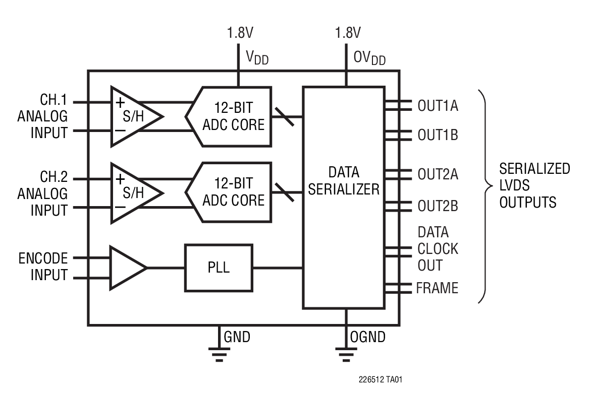
Analog Devices Inc.The LTC2265-12/LTC2264-12/LTC2263-12 are 2-channel, simultaneous sampling 12-bit A/D converters designed for digitizing high frequency, wide dynamic range signals. They are perfect for demanding communications applications with AC performance that includes 71dB SNR and 90dB spurious free dynamic range (SFDR). Ultralow jitter of 0.15psRMS allows undersampling of IF frequencies with excellent noise performance.DC specs include ±0.3LSB INL (typ), ±0.1LSB DNL (typ) and no missing codes over temperature. The transition noise is a low 0.3LSBRMS.The digital outputs are serial LVDS to minimize the number of data lines. Each channel outputs two bits at a time (2-lane mode) or one bit at a time (1-lane mode). The LVDS drivers have optional internal termination and adjustable output levels to ensure clean signal integrity.The ENC+ and ENC– inputs may be driven differentially or single-ended with a sine wave, PECL, LVDS, TTL, or CMOS inputs. An internal clock duty cycle stabilizer allows high performance at full speed for a wide range of clock duty cycles. Bits LTC2264-12 12 LTC2264-14 14 Applications Communications Cellular Base Stations Software Defined Radios Portable Medical Imaging Multichannel Data Acquisition Nondestructive Testing

DC1718A
Part Number : DC1718A
Analog Devices Inc.The LTC2471/LTC2473 are small, 16-bit analog-to-digital converters with an integrated precision reference and a selectable 208sps or 833sps output rate. They use a single 2.7V to 5.5V supply and communicate through an I2C Interface. The LTC2471 is single-ended with a 0V to VREF input range and the LTC2473 is differential with a ±VREF input range. Both ADCs include a 1.25V integrated reference with 2ppm/°C drift performance and 0.1% initial accuracy. The converters are available in a 12-pin DFN 3mm × 3mm package or an MSOP-12 package. They include an integrated oscillator and perform conversions with no latency for multiplexed applications. The LTC2471/LTC2473 include a proprietary input sampling scheme that reduces the average input current several orders of magnitude when compared to conventional delta sigma converters.Following a single conversion, the LTC2471/LTC2473 automatically power down the converter and can also be configured to power down the reference. When both the ADC and reference are powered down, the supply current is reduced to 200nA.The LTC2471/LTC2473 include a user selectable 208sps or 833sps output rate and due to a large oversampling ratio (8,192 at 208sps and 2,048 at 833sps) have relaxed anti-aliasing requirements.Applications System Monitoring Environmental Monitoring Direct Temperature Measurements Instrumentation Industrial Process Control Data Acquisition Embedded ADC Upgrades

DC1755A
Part Number : DC1755A
Analog Devices Inc.The LTC3860 is a dual, PolyPhase® synchronous stepdown switching regulator controller for high current distributed power systems, digital signal processors, and other telecom and industrial DC/DC power supplies. It uses a constant frequency voltage mode architecture combined with very low offset, high bandwidth error amplifiers and a remote output sense differential amplifier for excellent transient response and output regulation. The controller incorporates lossless inductor DCR current sensing to maintain current balance between phases and to provide overcurrent protection. The chip operates from a VCC supply between 3V and 5.5V and is designed for stepdown conversion from VIN between 3V and 24V to output voltages between 0.6V and VCC – 0.5V. The TRACK/SS pins provide programmable soft-start or tracking functions. Inductor current reversal is disabled during soft-start to safely power prebiased loads. The constant operating frequency can be synchronized to an external clock or linearly programmed from 250kHz to 1.25MHz. Up to six LTC3860 controllers can operate in parallel for 1-, 2-, 3-, 4-, 6- or 12-phase operation. The LTC3860 is available in a 32-pin 5mm × 5mm QFN package.Applications High Current Distributed Power Systems Digital Signal Processor and ASIC Supplies Telecom Systems Industrial Power Supplies

DC1762A-D
Part Number : DC1762A-D
Analog Devices Inc.The LTC2162/LTC2161/LTC2160 are sampling 16-bit A/D converters designed for digitizing high frequency, wide dynamic range signals. They are perfect for demanding communications applications with AC performance that includes 77dB SNR and 90dB spurious free dynamic range (SFDR). Ultralow jitter of 0.07psRMS allows undersampling of IF frequencies with excellent noise performance.DC specs include ±2LSB INL (typ), ±0.5LSB DNL (typ) and no missing codes over temperature. The transition noise is 3.3LSBRMS.The digital outputs can be either full rate CMOS, double data rate CMOS, or double data rate LVDS. A separate output power supply allows the CMOS output swing to range from 1.2V to 1.8V.The ENC+ and ENC– inputs may be driven differentially or single-ended with a sine wave, PECL, LVDS, TTL, or CMOS inputs. An optional clock duty cycle stabilizer allows high performance at full speed for a wide range of clock duty cycles.Applications Communications Cellular Base Stations Software Defined Radios Portable Medical Imaging Multichannel Data Acquisition Nondestructive Testing

DC1763A-F
Part Number : DC1763A-F
Analog Devices Inc.The LTC2192/LTC2191/LTC2190 are 2-channel, simultaneous sampling 16-bit A/D converters designed for digitizing high frequency, wide dynamic range signals. They are perfect for demanding communications applications with AC performance that includes 77dB SNR and 90dB spurious free dynamic range (SFDR). Ultralow jitter of 0.07psRMS allows undersampling of IF frequencies with excellent noise performance. DC specs include ±2LSB INL (typ), ±0.5LSB DNL (typ) and no missing codes over temperature. The transition noise is 3.3LSBRMS. To minimize the number of data lines the digital outputs are serial LVDS. Each channel outputs one bit, two bits or four bits at a time. The LVDS drivers have optional internal termination and adjustable output levels to ensure clean signal integrity. The ENC+ and ENC– inputs may be driven differentially or single ended with a sine wave, PECL, LVDS, TTL or CMOS inputs. An internal clock duty cycle stabilizer allows high performance at full speed for a wide range of clock duty cycles.Applications Communications Cellular Base Stations Software-Defined Radios Portable Medical Imaging Multi-Channel Data Acquisition Nondestructive Testing

AD5421BREZ
Part Number : AD5421BREZ
Analog Devices Inc.The AD5421 is a complete, loop-powered, 4 mA to 20 mAdigital-to-analog converter (DAC) designed to meet the needsof smart transmitter manufacturers in the industrial controlindustry. The DAC provides a high precision, fully integrated,low cost solution in compact TSSOP and LFCSP packages.The AD5421 includes a regulated voltage output that is used topower itself and other devices in the transmitter. This regulatorprovides a regulated 1.8 V to 12 V output voltage. The AD5421also contains 1.22 V and 2.5 V references, thus eliminating theneed for a discrete regulator and voltage reference.The AD5421 can be used with standard Highway AddressableRemote Transducer (HART®) FSK protocol communicationcircuitry without any degradation in specified performance. Thehigh speed serial interface is capable of operating at 30 MHz andallows for simple connection to commonly used microprocessorsand microcontrollers via a SPI-compatible, 3-wire interface.The AD5421 is guaranteed monotonic to 16 bits. It provides0.0015% integral nonlinearity, 0.0012% offset error, and0.0006% gain error under typical conditions.The AD5421 is available in a 28-lead TSSOP and a 32-lead LFCSPspecified over the extended industrial temperature range of−40°C to +105°C.Applications Industrial Process Control 4 mA to 20 mA loop-powered transmitters Smart transmitters HART network connectivity
AD5421CREZ
Part Number : AD5421CREZ
Analog Devices Inc.The AD5421 is a complete, loop-powered, 4 mA to 20 mAdigital-to-analog converter (DAC) designed to meet the needsof smart transmitter manufacturers in the industrial controlindustry. The DAC provides a high precision, fully integrated,low cost solution in compact TSSOP and LFCSP packages.The AD5421 includes a regulated voltage output that is used topower itself and other devices in the transmitter. This regulatorprovides a regulated 1.8 V to 12 V output voltage. The AD5421also contains 1.22 V and 2.5 V references, thus eliminating theneed for a discrete regulator and voltage reference.The AD5421 can be used with standard Highway AddressableRemote Transducer (HART®) FSK protocol communicationcircuitry without any degradation in specified performance. Thehigh speed serial interface is capable of operating at 30 MHz andallows for simple connection to commonly used microprocessorsand microcontrollers via a SPI-compatible, 3-wire interface.The AD5421 is guaranteed monotonic to 16 bits. It provides0.0015% integral nonlinearity, 0.0012% offset error, and0.0006% gain error under typical conditions.The AD5421 is available in a 28-lead TSSOP and a 32-lead LFCSPspecified over the extended industrial temperature range of−40°C to +105°C.Applications Industrial Process Control 4 mA to 20 mA loop-powered transmitters Smart transmitters HART network connectivity

AD5541ABCPZ-REEL7
Part Number : AD5541ABCPZ-REEL7
Analog Devices Inc.The AD5541A is a single, 16-bit, serial input, unbuffered voltage output digital-to-analog converter (DAC) that operate from a single 2.7 V to 5.5 V supply.The DAC output range extends from 0 V to VREF and is guaranteed monotonic, providing ±1 LSB INL accuracy at 16 bits without adjustment over the full specified temperature range of −40°C to +125°C. The AD5541A is available in a 3 mm × 3 mm, 10-lead LFCSP and 10-lead MSOP. The AD5541A-1 is available in a 3 mm × 3 mm, 8-lead LFCSP.Offering unbuffered outputs, the AD5541A achieves a 1 μs set-tling time with low power consumption and low offset errors. Providing low noise performance of 11.8 nV/√Hz and low glitch, the AD5541A is suitable for deployment across multiple end systems.The AD5541A uses a versatile 3-wire interface that is compatible with a 50 MHz SPI, QSPI™, MICROWIRE™, and DSP interface standards.PRODUCT HIGHLIGHTS 16-bit performance without adjustment. 2.7 V to 5.5 V single operation. Low 11.8 nV/√Hz noise spectral density. Low 0.05 ppm/°C temperature drift. 3 mm × 3 mm LFCSP and MSOP packaging.Applications Automatic test equipment Precision Source-measure Instruments Data Acquisition Systems Medical Instrumentation Aerospace Instrumentation Communications Infrastructure equipment Industrial Control

AD7291BCPZ
Part Number : AD7291BCPZ
Analog Devices Inc.The AD7291 is a 12-bit, low power, 8-channel, successive approximation analog-to-digital converter (ADC) with an internal temperature sensor.The part operates from a single 3.3 V power supply and features an I2C-compatible interface. The part contains a 9-channel multiplexer and a track-and-hold amplifier than can handle frequencies up to 30 MHz. The device has an on-chip 2.5 V reference that can be disabled to allow the use of an external reference.The AD7291 provides a 2-wire serial interface compatible with I2C interfaces. The I2C interface supports standard and fast I2C interface modes. The AD7291 normally remains in a partial power-down state while not converting and powers up for conversions. The conversion process can be controlled by a command mode where conversions occur across I2C write operations or an autocycle mode selected through software control.The AD7291 includes a high accuracy band gap temperature sensor, which is monitored and digitized by the 12-bit ADC to give a resolution of 0.25°C.The AD7291 offers a programmable sequencer, which enables the selection of a preprogrammable sequence of channels for conversion.On-chip limit registers can be programmed with high and low limits for the conversion results; an out-of-range indicator output (ALERT) becomes active when the programmed high or low limits are violated by the conversion result. This output can be used as an interrupt. Product HighlightsIdeally suited to monitoring system variables in a variety of systems including telecommunications, process control, and industrial control.I2C-compatible serial interface. Standard and fast modes.Automatic partial power-down while not converting to maximize power efficiency.Channel sequencer operation.Integrated temperature sensor with 0.25°C resolution.Out of range indicator that can be software disabled or enabled.

AD8227ARMZ-R7
Part Number : AD8227ARMZ-R7
Analog Devices Inc.The AD8227 is a low cost, wide supply range instrumentation amplifier that requires only one external resistor to set any gain between 5 and 1000.The AD8227 is designed to work with a variety of signal voltages. A wide input range and rail-to-rail output allow the signal to make full use of the supply rails. Because the input range can also go below the negative supply, small signals near ground can be amplified without requiring dual supplies. The AD8227 operates on supplies ranging from ±1.5 V to ±18 V (2.2 V to 36 V single supply).The robust AD8227 inputs are designed to connect to real-world sensors. In addition to its wide operating range, the AD8227 can handle voltages beyond the rails. For example, with a ±5 V supply, the part is guaranteed to withstand ±35 V at the input with no damage. Minimum as well as maximum input bias currents are specified to facilitate open wire detection.The AD8227 is ideal for multichannel, space-constrained applications. With its MSOP package and 125°C temperature rating, the AD8227 thrives in tightly packed, zero airflow designs.The AD8227 is available in 8-pin MSOP and SOIC packages. It is fully specified for −40°C to +125°C operation.For a similar instrumentation amplifier with a gain range of 1 to 1000, see the AD8226.ApplicationsIndustrial process controlsBridge amplifiersMedical instrumentationPortable data acquisitionMultichannel systems

AD8475BRMZ
Part Number : AD8475BRMZ
Analog Devices Inc.The AD8475 is a fully differential, attenuating amplifier with integrated precision gain resistors. It provides precision attenuation (by 0.4 or 0.8), common-mode level shifting, and single-ended-to-differential conversion along with input overvoltage protection. Power dissipation on a single 5 V supply is only 16 mW.The AD8475 is a simple to use, fully integrated precision gain block, designed to process signal levels of up to ±10 V on a single supply. It provides a complete interface to make industrial level signals directly compatible with the differential input ranges of low voltage high performance 16-bit or 18-bit single-supply successive approximation (SAR) analog-to-digital converters (ADCs).The AD8475 comes with two standard pin-selectable gain options: 0.4 and 0.8. The gain of the part is set by driving the input pin corresponding to the appropriate gain.The AD8475 also provides overvoltage protection from large industrial input voltages up to ±15 V while operating on a single 5 V supply. The VOCM pin adjusts the output voltage common mode for precision level shifting, to match the ADC’s input range and maximize dynamic range.The AD8475 works extremely well with SAR, Σ-Δ, and pipeline converters. The high current output stage of the part allows it to drive the switched capacitor front-end circuits of many ADCs with minimal error.Unlike many differential drivers in the market, the AD8475 is a high precision amplifier. With 500 μV maximum output offset, 10 nV/√Hz output noise, and −112 dB THD + N, the AD8475 pairs well with high accuracy converters. Considering its low power consumption and high precision, the slew-enhanced AD8475 has excellent speed, settling to 18-bit precision for 4 MSPS acquisition.The AD8475 is available in a space-saving 16-lead 3 mm × 3 mm LFCSP package and a 10-lead MSOP package. It is fully specified over the −40°C to +85°C temperature range.Applications ADC drivers Differential instrumentation amplifier building blocks Single-ended-to-differential converters

AD8657ARMZ
Part Number : AD8657ARMZ
Analog Devices Inc.The AD8657/AD8659 are dual and quad micropower, precision,rail-to-rail input/output amplifiers optimized for low power and wide operating supply voltage range applications.The AD8657/AD8659 operate from 2.7 V to 18 V with a typicalquiescent supply current of 18 μA. The devices use the AnalogDevices, Inc., patented DigiTrim® trimming technique, whichachieves low offset voltage. The AD8657/AD8659 also have high immunity to electromagnetic interference.The combination of low supply current, low offset voltage, very low input bias current, wide supply range, and rail-to-rail input and output make the AD8657/AD8659 ideal for currentmonitoring in process and motor control applications. Thecombination of precision specifications makes these devicesideal for dc gain and buffering of sensor front ends or high impedance input sources in wireless or remote sensors or transmitters.The AD8657/AD8659 are specified over the extended industrial temperature range (−40°C to +125°C). The AD8657 is available in an 8-lead MSOP package and an 8-lead LFCSP package; the AD8659 is available in a 14-lead SOIC package and 16-leadLFCSP package.Applications Portable operating systems Current monitors 4 mA to 20 mA loop drivers Buffer/level shifting Multipole filters Remote/wireless sensors Low power transimpedance amplifiers

AD9125BCPZRL
Part Number : AD9125BCPZRL
Analog Devices Inc.The AD9125 is a dual, 16-bit, high dynamic range TxDAC+® digital-to-analog converter (DAC) that provides a sample rate of 1000 MSPS, permitting a multicarrier generation up to the Nyquist frequency. It includes features optimized for direct conversion transmit applications, including complex digital modulation, and gain and offset compensation. The DAC outputs are optimized to interface seamlessly with analog quadrature modulators, such as the ADL537x F-MOD series from Analog Devices, Inc. A 4-wire serial port interface allows programming/readback of many internal parameters. Full-scale output current can be programmed over a range of 8.7 mA to 31.7 mA. The AD9125 comes in a 72-lead LFCSP.PRODUCT HIGHLIGHTS Ultralow noise and intermodulation distortion (IMD) enable high quality synthesis of wideband signals from baseband to high intermediate frequencies. A proprietary DAC output switching technique enhances dynamic performance. The current outputs are easily configured for various single-ended or differential circuit topologies. Flexible CMOS digital interface allows the standard 32-wire bus to be reduced to a 16-wire bus.APPLICATIONS Wireless infrastructure W-CDMA, CDMA2000, TD-SCDMA, WiMAX, GSM, LTE Digital high or low IF synthesis Transmit diversity Wideband communications: LMDS/MMDS, point-to-point Cable modem termination systems

AD9523BCPZ
Part Number : AD9523BCPZ
Analog Devices Inc.The AD9523 provides a low power, multi-output, clock distribution function with low jitter performance, along with an on-chip PLL and VCO. The on-chip VCO tunes from 3.6 GHz to 4.0 GHz.The AD9523 is designed to support the clock requirements for long term evolution (LTE) and multicarrier GSM base station designs. It relies on an external VCXO to provide the reference jitter cleanup to achieve the restrictive low phase noise requirements necessary for acceptable data converter SNR performance.The input receivers, oscillator, and zero delay receiver provide both single-ended and differential operation. When connected to a recovered system reference clock and a VCXO, the device generates 14 low noise outputs with a range of 1 MHz to 1 GHz, and one dedicated buffered output from the input PLL (PLL1). The frequency and phase of one clock output relative to another clock output can be varied by means of a divider phase select function that serves as a jitter-free coarse timing adjustment in increments that are equal to the period of the signal coming out of the VCO.An in-package EEPROM can be programmed through the serial interface to store user-defined register settings for power-up and chip reset.APPLICATIONS LTE and multicarrier GSM base stations Wireless and broadband infrastructure Medical instrumentation Clocking high speed ADCs, DACs, DDSs, DDCs, DUCs, MxFEs Low jitter, low phase noise clock distribution Clock generation and translation for SONET, 10Ge, 10G FC, and other 10 Gbps protocols Forward error correction (G.710) High performance wireless transceivers ATE and high performance instrumentation

AD9789BBCZ
Part Number : AD9789BBCZ
Analog Devices Inc.The AD9789 is a flexible QAM encoder/interpolator/upconverter combined with a high performance, 2400 MSPS, 14-bit RF digital-to-analog converter (DAC). The flexible digital interface can accept up to four channels of complex data. The QAM encoder supports constellation sizes of 16, 32, 64, 128, and 256 with SRRC filter coefficients for all standards.The on-chip rate converter supports a wide range of baud rates with a fixed DAC clock. The digital upconverter can place the channels from 0 to 0.5 × fDAC. This permits four contiguous channels to be synthesized and placed anywhere from dc to fDAC.The AD9789 includes a serial peripheral interface (SPI) for device configuration and status register readback. The flexible digital interface can be configured for data bus widths of 4, 8, 16, and 32 bits. It can accept real or complex data.The AD9789 operates from 1.5 V, 1.8 V, and 3.3 V supplies for a total power consumption of 1.6 W. It is supplied in a 164-ball chip scale package ball grid array for lower thermal impedance and reduced package parasitics. No special power sequencing is required. The clock receiver powers up muted to prevent start-up noise.Product Highlights Highly integrated and configurable QAM mappers, interpolators, and upconverters for direct synthesis of one to four DOCSIS- or DVB-C-compatible channels in a block. Low noise and intermodulation distortion (IMD) performance enable high quality synthesis of signals up to 1 GHz. Flexible data interface supports LVDS for improved SFDR or CMOS input data for less demanding applications. Interface is configurable from 4-bit nibbles to 32-bit words and can run at up to 150 MHz CMOS or 150 MHz LVDS double data rate (DDR). Manufactured on a CMOS process, the AD9789 uses a proprietary switching technique that enhances dynamic performance.Applications Broadband communications systems CMTS/DVB Cellular infrastructure Point-to-point wireless

ADA4691-4ACPZ-R2
Part Number : ADA4691-4ACPZ-R2
Analog Devices Inc.The ADA4691-2/ADA4692-2 are dual and the ADA4691-4/ADA4692-4 are the quad rail-to-rail output, single-supply amplifiers featuring low power, wide bandwidth, and low noise. The ADA4691-2 has two independent shutdown pins, allowing further reduction in supply current. The ADA4691-4 is a quad with dual shutdown pins each controlling a pair of amplifiers and is available in the 16-lead LFCSP. The ADA4692-4 is a quad version without shutdown.These amplifiers are ideal for a wide variety of applications. Audio, filters, photodiode amplifiers, and charge amplifiers, all benefit from this combination of performance and features. Additional applications for these amplifiers include portable consumer audio players with low noise and low distortion that provide high gain and slew rate response over the audio band at low power. Industrial applications with high impedance sensors, such as pyroelectric and IR sensors, benefit from the high impedance and low 0.5 pA input bias, low offset drift, and enough bandwidth and response for low gain applications.The ADA4691/ADA4692 family is fully specified over the extended industrial temperature range (−40°C to +125°C). The ADA4691-2 is available in a 10-lead LFCSP and a 9-ball WLCSP. The ADA4692-2 is available in an 8-lead SOIC and 8-lead LFCSP. The ADA4691-4 is available in a 16-lead LFCSP. The ADA4692-4 is available in a 14-lead TSSOP. Applications Photodiode amplifiers Sensor amplifiers Portable medical and instrumentation Portable audio: MP3s, PDAs, and smartphones Communications Low-side current sense ADC driver Active filters Sample-and-hold

ADA4891-2ARMZ
Part Number : ADA4891-2ARMZ
Analog Devices Inc.The ADA4891-1 (single), ADA4891-2 (dual), ADA4891-3 (triple), and ADA4891-4 (quad) are CMOS, high speed amplifiers that offer high performance at a low cost. The amplifiers feature true single-supply capability, with an input voltage range that extends 300 mV below the negative rail. In spite of their low cost, the ADA4891 family provides high performance and versatility. The rail-to-rail output stage enables the output to swing within 50 mV of each rail, enabling maximum dynamic range. The ADA4891 family of amplifiers is ideal for imaging applications, such as consumer video, CCD buffers, and contact image sensor buffers. Low distortion and fast settling time also make them ideal for active filter applications. The ADA4891-1/ADA4891-2/ADA4891-3/ADA4891-4 are available in a wide variety of packages. The ADA4891-1 is available in 8-lead SOIC and 5-lead SOT-23 packages. The ADA4891-2 is available in 8-lead SOIC and 8-lead MSOP packages. The ADA4891-3 and ADA4891-4 are available in 14-lead SOIC and 14-lead TSSOP packages. The amplifiers are specified to operate over the extended temperature range of −40°C to +125°C.Applications Imaging Consumer video Active filters Coaxial cable drivers Clock buffers Photodiode preamp Contact image sensor and buffers

AD823AARZ-RL
Part Number : AD823AARZ-RL
Analog Devices Inc.The AD823A is a dual precision, 17 MHz, JFET input op amp manufactured in the extra fast complementary bipolar (XFCB) process. The AD823A can operate from a single supply of 3 V to 36 V or from dual supplies of ±1.5 V to ±18 V. It has true single-supply capability with an input voltage range extending below ground in single-supply mode. Output voltage swing extends to within 20 mV of each rail for IOUT ≤ 100 μA, providing outstanding output dynamic range. It also has a linear output current of 40 mA, 0.5 V from the supply rails.An offset voltage of 700 μV maximum, an offset voltage drift of 1 μV/°C, and typical input bias currents of 0.3 pA provide dc precision with source impedances up to 1 GΩ. The AD823A provides 17 MHz, −3 dB bandwidth, and a 30 V/μs slew rate with a low supply current of only 2.6 mA per amplifier. It also provides low input voltage noise of 14 nV/√Hz and −108 dB SFDR at 20 kHz. The AD823A has low input capacitances (0.6 pF differential and 1.3 pF common mode) and drives more than 500 pF of direct capacitive load as a follower. This lets the amplifier handle a wide range of load conditions.This combination of ac and dc performance, plus the outstanding load drive capability, results in an exceptionally versatile amplifier for applications such as ADC drivers, high speed active filters, and other low voltage, high dynamic range systems.The AD823A is available over the industrial temperature range of −40°C to +85°C and is offered in an 8-lead SOIC package and an 8-lead MSOP package.APPLICATIONS Battery-powered precision instrumentation Photodiode preamps Active filters 12-bit to 16-bit data acquisition systems Medical instrumentation

AD9648-125EBZ
Part Number : AD9648-125EBZ
Analog Devices Inc.The AD9648 is a monolithic, dual-channel, 1.8 V supply, 14-bit, 105 MSPS/125 MSPS analog-to-digital converter (ADC). It features a high performance sample-and-hold circuit and on-chip voltage reference. The product uses multistage differential pipeline architecture with output error correction logic to provide 14-bit accuracy at 125 MSPS data rates and to guarantee no missing codes over the full operating temperature range.The ADC contains several features designed to maximize flexibility and minimize system cost, such as programmable clock and data alignment and programmable digital test pattern generation. The available digital test patterns include built-in deterministic and pseudorandom patterns, along with custom user-defined test patterns entered via the serial port interface (SPI).A differential clock input controls all internal conversion cycles. An optional duty cycle stabilizer (DCS) compensates for wide variations in the clock duty cycle while maintaining excellent overall ADC performance.The digital output data is presented in offset binary, Gray code, or twos complement format. A data output clock (DCO) is provided for each ADC channel to ensure proper latch timing with receiving logic. Output logic levels of 1.8 V CMOS or LVDS are supported. Output data can also be multiplexed onto a single output bus.The AD9648 is available in a 64-lead RoHS compliant LFCSP and is specified over the industrial temperature range (−40°C to +85°C). Applications Communications Diversity radio systems Multimode digital receivers GSM, EDGE, W-CDMA, LTE, CDMA2000, WiMAX, TD-SCDMA I/Q demodulation systems Smart antenna systems Broadband data applications Battery-powered instruments Hand held scope meters Portable medical imaging Ultrasound Radar/LIDARProduct Highlights The AD9648 operates from a single 1.8 V analog power supply and features a separate digital output driver supply to accommodate 1.8 V CMOS or LVDS logic families. The patented sample-and-hold circuit maintains excellent performance for input frequencies up to 200 MHz and is designed for low cost, low power, and ease of use. A standard serial port interface supports various product features and functions, such as data output formatting, internal clock divider, power-down, DCO/data timing and offset adjustments. The AD9648 is packaged in a 64-lead RoHS compliant LFCSP that is pin compatible with the AD9650/AD9269/AD9268 16-bit ADC’s, the AD9258 14-bit ADC, the AD9628/AD9231 12-bit ADC’s, and the AD9608/AD9204 10-bit ADC’s, enabling a simple migration path between 10-bit and 16-bit converters sampling from 20 MSPS to 125 MSPS.
AD9648BCPZ-105
Part Number : AD9648BCPZ-105
Analog Devices Inc.The AD9648 is a monolithic, dual-channel, 1.8 V supply, 14-bit, 105 MSPS/125 MSPS analog-to-digital converter (ADC). It features a high performance sample-and-hold circuit and on-chip voltage reference. The product uses multistage differential pipeline architecture with output error correction logic to provide 14-bit accuracy at 125 MSPS data rates and to guarantee no missing codes over the full operating temperature range.The ADC contains several features designed to maximize flexibility and minimize system cost, such as programmable clock and data alignment and programmable digital test pattern generation. The available digital test patterns include built-in deterministic and pseudorandom patterns, along with custom user-defined test patterns entered via the serial port interface (SPI).A differential clock input controls all internal conversion cycles. An optional duty cycle stabilizer (DCS) compensates for wide variations in the clock duty cycle while maintaining excellent overall ADC performance.The digital output data is presented in offset binary, Gray code, or twos complement format. A data output clock (DCO) is provided for each ADC channel to ensure proper latch timing with receiving logic. Output logic levels of 1.8 V CMOS or LVDS are supported. Output data can also be multiplexed onto a single output bus.The AD9648 is available in a 64-lead RoHS compliant LFCSP and is specified over the industrial temperature range (−40°C to +85°C). Applications Communications Diversity radio systems Multimode digital receivers GSM, EDGE, W-CDMA, LTE, CDMA2000, WiMAX, TD-SCDMA I/Q demodulation systems Smart antenna systems Broadband data applications Battery-powered instruments Hand held scope meters Portable medical imaging Ultrasound Radar/LIDARProduct Highlights The AD9648 operates from a single 1.8 V analog power supply and features a separate digital output driver supply to accommodate 1.8 V CMOS or LVDS logic families. The patented sample-and-hold circuit maintains excellent performance for input frequencies up to 200 MHz and is designed for low cost, low power, and ease of use. A standard serial port interface supports various product features and functions, such as data output formatting, internal clock divider, power-down, DCO/data timing and offset adjustments. The AD9648 is packaged in a 64-lead RoHS compliant LFCSP that is pin compatible with the AD9650/AD9269/AD9268 16-bit ADC’s, the AD9258 14-bit ADC, the AD9628/AD9231 12-bit ADC’s, and the AD9608/AD9204 10-bit ADC’s, enabling a simple migration path between 10-bit and 16-bit converters sampling from 20 MSPS to 125 MSPS.


