
DC1565A-C
Part Number : DC1565A-C
Analog Devices Inc.The LTC2152-14/LTC2151-14/LTC2150-14 are 250Msps/210Msps/170Msps 14-bit A/D converters designed for digitizing high frequency, wide dynamic range signals. They are perfect for demanding communications applications with AC performance that includes 70dB SNR and 90dB spurious free dynamic range (SFDR). The 1.25GHz input bandwidth allows the ADC to undersample high frequencies with good performance. The latency is only five clock cycles.DC specs include ±0.85LSB INL (typ), ±0.25LSB DNL (typ) and no missing codes over temperature. The transition noise is 1.82LSBRMS.The digital outputs are double-data rate (DDR) LVDS.The ENC+ and ENC– inputs can be driven differentially with a sine wave, PECL, LVDS, TTL, or CMOS inputs. An optional clock duty cycle stabilizer allows high performance at full speed for a wide range of clock duty cycles. Bits LTC2150-12 12 LTC2150-14 14 Applications Communications Cellular Basestations Software Defined Radios Medical Imaging High Definition Video Testing and Measurement Instruments

DC1620A-N
Part Number : DC1620A-N
Analog Devices Inc.The LTC2145-12/LTC2144-12/LTC2143-12 are 2-channel simultaneous sampling 12-bit A/D converters designed for digitizing high frequency, wide dynamic range signals. They are perfect for demanding communications applications with AC performance that includes 70.6dB SNR and 89dB spurious free dynamic range (SFDR). Ultralow jitter of 0.08psRMS allows undersampling of IF frequencies with excellent noise performance.DC specs include ±0.3LSB INL (typ), ±0.1LSB DNL (typ) and no missing codes over temperature. The transition noise is 0.3LSBRMS.The digital outputs can be either full rate CMOS, double data rate CMOS, or double data rate LVDS. A separate output power supply allows the CMOS output swing to range from 1.2V to 1.8V.The ENC+ and ENC– inputs may be driven differentially or single-ended with a sine wave, PECL, LVDS, TTL, or CMOS inputs. An optional clock duty cycle stabilizer allows high performance at full speed for a wide range of clock duty cycles. Bits LTC2144-12 12 LTC2144-14 14 Applications Communications Cellular Base Stations Software Defined Radios Portable Medical Imaging Multi-Channel Data Acquisition Nondestructive Testing

DC1774A-C
Part Number : DC1774A-C
Analog Devices Inc.The LTC6431-15 is a gain-block amplifier with excellent linearity at frequencies beyond 1000MHz and with low associated output noise.The unique combination of high linearity, low noise and low power dissipation make this an ideal candidate for many signal-chain applications. The LTC6431-15 is easy to use, requiring a minimum of external components. It is internally input/output matched to 50Ω and it draws only 90mA from a single 5V supply.On-chip bias and temperature compensation maintain performance over environmental changes.The LTC6431-15 uses a high performance SiGe BiCMOS process for excellent repeatability compared with similar GaAs amplifiers. All A-grade LTC6431-15 devices are tested and guaranteed for OIP3 at 240MHz. The LTC6431-15 is housed in a 4mm x 4mm 24-lead QFN package with an exposed pad for thermal management and low inductance.Applications Single-Ended IF Amplifier ADC Driver CATV

DC1783A-H
Part Number : DC1783A-H
Analog Devices Inc.The LTC2376-18 is a low noise, low power, high speed 18-bit successive approximation register (SAR) ADC. Operating from a 2.5V supply, the LTC2376-18 has a ±VREF fully differential input range with VREF ranging from 2.5V to 5.1V. The LTC2376-18 consumes only 3.4mW and achieves ±1.75LSB INL maximum, no missing codes at 18 bits with 102dB SNR.The LTC2376-18 has a high speed SPI-compatible serial interface that supports 1.8V, 2.5V, 3.3V and 5V logic while also featuring a daisy-chain mode. The fast 250ksps throughput with no cycle latency makes the LTC2376-18 ideally suited for a wide variety of high speed applications. An internal oscillator sets the conversion time, easing external timing considerations. The LTC2376-18 automatically powers down between conversions, leading to reduced power dissipation that scales with the sampling rate.The LTC2376-18 features a unique digital gain compression (DGC) function, which eliminates the driver amplifier’s negative supply while preserving the full resolution of the ADC. When enabled, the ADC performs a digital scaling function that maps zero-scale code from 0V to 0.1 • VREF and full-scale code from VREF to 0.9 • VREF. For a typical reference voltage of 5V, the full-scale input range is now 0.5V to 4.5V, which provides adequate headroom for powering the driving amplifier from a single 5.5V supply.Applications Medical Imaging High Speed Data Acquisition Portable or Compact Instrumentation Industrial Process Control Low Power Battery-Operated Instrumentation ATE
DC1796A-F
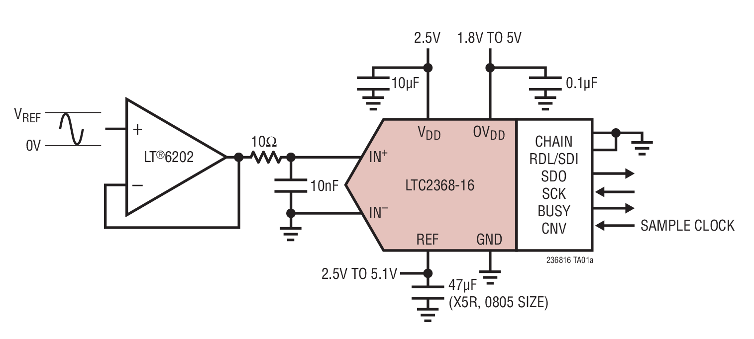
Part Number : DC1796A-F
Analog Devices Inc.The LTC2368-16 is a low noise, low power, high speed 16-bit successive approximation register (SAR) ADC. Operating from a 2.5V supply, the LTC2368-16 has a 0V to VREF pseudo-differential unipolar input range with VREF ranging from 2.5V to 5.1V. The LTC2368-16 consumes only 13.5mW and achieves ±0.75LSB INL maximum, no missing codes at 16 bits with 94.7dB SNR.The LTC2368-16 has a high speed SPI-compatible serial interface that supports 1.8V, 2.5V, 3.3V and 5V logic while also featuring a daisy-chain mode. The fast 2Msps throughput with no cycle latency makes the LTC2368-16 ideally suited for a wide variety of high speed applications. An internal oscillator sets the conversion time, easing external timing considerations. The LTC2368-16 automatically powers down between conversions, leading to reduced power dissipation that scales with the sampling rate.Applications Medical Imaging High Speed Data Acquisition Portable or Compact Instrumentation Industrial Process Control Low Power Battery-Operated Instrumentation ATE

DC1856B-B
Part Number : DC1856B-B
Analog Devices Inc.The LTM4649 is a complete 10A high efficiency switching mode step-down DC/DC μModule® regulator in a 9mm × 15mm × 4.92 BGA package. Included in the package are the switching controller, power FETs, inductor, and all support components. Operating over an input voltage range of 4.5V to 16V, the LTM4649 supports an output voltage range of 0.6V to 3.3V, set by a single external resistor. This high efficiency design delivers 10A continuous current. Only bulk input and output capacitors are needed.High switching frequency and a current mode architecture enable a very fast transient response to line and load changes without sacrificing stability. The device supports frequency synchronization, programmable multiphase operation, and output voltage tracking for supply rail sequencing.Fault protection features include output overvoltage and overcurrent protection. The LTM4649 is offered in a small 9mm × 15mm × 4.92mm BGA package available with SnPb or RoHS compliant terminal finish.Applications Telecom, Networking and Industrial Equipment Point of Load Regulation

DC1889A
Part Number : DC1889A
Analog Devices Inc.The LTM4624 is a complete 4A step-down switching mode μModule® (micromodule) regulator in a tiny 6.25mm × 6.25mm × 5.01mm BGA package. Included in the package are the switching controller, power FETs, inductor and support components. Operating over an input voltage range of 4V to 14V or 2.375V to 14V with an external bias supply, the LTM4624 supports an output voltage range of 0.6V to 5.5V, set by a single external resistor. Its high efficiency design delivers 4A continuous, 5A peak, output current. Only bulk input and output capacitors are needed.The LTM4624 supports selectable discontinuous mode operation and output voltage tracking for supply rail sequencing. Its high switching frequency and current mode control enable a very fast transient response to line and load changes without sacrificing stability.Fault protection features include overvoltage, overcurrent and overtemperature protection.The LTM4624 is available with SnPb (BGA) or RoHS compliant terminal finish.APPLICATIONS Telecom, Datacom, Networking and Industrial Equipment Medical Diagnostic Equipment Data Storage Rack Units and Cards Test and Debug Systems

DC1926A
Part Number : DC1926A
Analog Devices Inc.The LTC4353 controls external N-channel MOSFETs to implement an ideal diode function. It replaces two high power Schottky diodes and their associated heat sinks, saving power and board area. The ideal diode function permits low loss power supply ORing and supply holdup applications.The LTC4353 regulates the forward-voltage drop across the MOSFET to ensure smooth current transfer in diode-OR applications. A fast turn-on reduces the load voltage droop during supply switchover. If the input supply fails or is shorted, a fast turn-off minimizes reverse-current transients.The controller operates with supplies from 2.9V to 18V. If both supplies are below 2.9V, an external supply is needed at the VCC pin. Enable inputs can be used to turn off the MOSFET and put the controller in a low current state. Status outputs indicate whether the MOSFETs are on or off.Applications Redundant Power Supplies Supply Holdup High Availability Systems and Servers Telecom and Network Infrastructure

DC1931B
Part Number : DC1931B
Analog Devices Inc.The LTM9013 is a 300MHz wideband, low IF receiver. Utilizing an integrated system in a package (SiP) technology, it is a μModule® (micromodule) receiver that includes a dual high speed 14-bit A/D converter, lowpass filter, differential gain stages and a quadrature demodulator.The LTM9013 is perfect for wideband I/Q receiver applications, with AC performance that includes 59dB SNR and 1.3dB frequency flatness from DC to 300MHz. A highpass filter or simple AC coupling are used external to the device for design flexiblity. The integrated on-chip broadband transformers provide a 50Ω single-ended interface at the RF input.A 5V supply powers the demodulator and a 3.3V supply powers the IF amplifiers for minimal distortion. A 1.8V supply allows low power ADC operation. A separate output supply allows the DDR LVDS outputs to drive 1.8V logic. An optional multiplexer allows both channels to share a digital output bus. An optional clock duty cycle stabilizer allows high performance at full speed for a wide range of clock duty cycles.Applications Telecommunications Wideband, Low IF Receivers Digital Predistortion Receivers Cellular Base Stations

DC1957A
Part Number : DC1957A
Analog Devices Inc.The LTM2892 is a complete galvanic digital μModule® (micromodule) isolator. No external components are required. Individual 3V to 5.5V supplies power each side of the digital isolator. Separate logic supply pins allow easy interfacing with different logic levels from 1.62V to 5.5V, independent of the main supply.Module options are available with compatibility to SPI (LTM2892-S) and I2C (LTM2892-I), master mode only, specifications.Coupled inductors provide 3500VRMS of isolation between the input and output logic interface. This device is ideal for systems where the ground loop is broken, allowing uninterrupted communication through large common mode transients faster than 50kV/μs.Applications Isolated SPI or I2C Interfaces Industrial Systems Test and Measurement Equipment Breaking Ground Loops

DC1978A
Part Number : DC1978A
Analog Devices Inc.The LTC2974 is a 4-channel Power System Manager used to sequence, trim (servo), margin, supervise, manage faults, provide telemetry and create fault logs. PMBus commands support power supply sequencing, precision point-of-load voltage adjustment and margining. DACs use a proprietary soft-connect algorithm to minimize supply disturbances. Supervisory functions include over and under current, voltage and temperature threshold limits for four power supply output channels as well as over and under voltage threshold limits for a single power supply input channel. Programmable fault responses can disable the power supplies with optional retry after a fault is detected. Faults that disable a power supply can automatically trigger black box EEPROM storage of fault status and associated telemetry. An internal 16-bit ADC monitors four output voltages, four output currents, four external temperatures, one input voltage and die temperature. Output power is also calculated. A programmable watchdog timer monitors microprocessor activity for a stalled condition and resets the microprocessor if necessary. A single wire bus synchronizes power supplies across multiple LTC Power System Management (PSM) devices. Configuration EEPROM with ECC supports autonomous operation without additional software.APPLICATIONS Computers and Network Servers Industrial Test and Measurement High Reliability Systems Medical Imaging Video

DC9018A-C
Part Number : DC9018A-C
Analog Devices Inc.SmartMesh WirelessHART wireless sensor networks are self managing, low power networks built from wireless nodes called motes. The LTC5800-WHM is the WirelessHART Mote-on-Chip™ integrated circuit in the Eterna® family of IEEE 802.15.4 System-on-Chip (SoC) solutions, featuring a highly integrated, low power radio design by Analog Devices as well as an ARM Cortex-M3 32-bit microprocessor running our embedded SmartMesh WirelessHART networking software.With Analog Devices' time-synchronized WirelessHART networks all motes in the network may route, source or terminate data while providing many years of battery powered operation. The SmartMesh WirelessHART software provided with the LTC5800-WHM is fully tested and validated, and is readily configured via a software Application Programming Interface.SmartMesh WirelessHART motes deliver a highly flexible network with proven reliability and low power performance in an easy-to-integrate platform. Network Features Feature Benefit Time Synchronized, Channel Hopping Communications >99.999% network reliability in even the most challenging RF environments Sub 50 µA Routers Can build out a network without any line powered devices. Flexibility to be line powered or energy harvested if desired. Secure Mesh with 128-bit AES Encryption NIST Certified Security. Compromise of one node does not compromise network. Standards-based Compliant to international standard IEC 62591 (WirelessHART) Highly Accurate Time Stamping Time stamping on every node is available to applications with millisecond accuracy Device Features Feature Benefit Industry-Leading Low Power Radio Technology 4.5mA to Receive a Packet 5.4mA to Transmit at 0dBm 9.7mA to Transmit at 8dBm Pre-engineered RF RF elements include an on-chip power amplifier and are pre-tuned for optimized performance, including temperature compensation, saving development time. Energy Harvesting Support Very low power design enables motes to be powered by a wide variety of energy harvesters ApplicationsLearn more about SmartMesh applications.

EVAL-AD5700-1EBZ
Part Number : EVAL-AD5700-1EBZ
Analog Devices Inc.The AD5700/AD5700-1 are single-chip solutions, designedand specified to operate as a HART® FSK half-duplex modem,complying with the HART physical layer requirements. TheAD5700/AD5700-1 integrate all of the necessary filtering, signaldetection, modulating, demodulating and signal generationfunctions, thus requiring few external components. The 0.5%precision internal oscillator on the AD5700-1 greatly reducesthe board space requirements, making it ideal for line-poweredapplications in both master and slave configurations. The maximumsupply current consumption is 115µA, making theAD5700/AD5700-1 an optimal choice for low power loop-powered applications.Transmit waveforms are phase continuous 1200 Hz and2200 Hz sinusoids. The AD5700/AD5700-1 contain accuratecarrier detect circuitry and use a standard UART interface.Applications Field transmitters HART multiplexers PLC and DCS analog I/O modules HART network connectivity

EVAL-ADM3051EBZ
Part Number : EVAL-ADM3051EBZ
Analog Devices Inc.The ADM3051 is a controller area network (CAN) physicallayer transceiver allowing a protocol layer CAN controller toaccess the physical layer bus. The ADM3051 complies withthe ISO 11898 standard. It is capable of running at data rates upto 1 Mbps.The device has current-limiting and thermal shutdown featuresto protect against output short circuits and situations where thebus may be shorted to ground or power terminals in 24 V buspower systems. The part is fully specified over the industrialtemperature range of −40°C to +125°C and is available in an8-lead SOIC package.Three operating modes are available: high speed, slope control,and standby. Pin 8 (RS) is used to select the operating mode.The low current standby mode can be selected by applying alogic high to RS.The device can be set to operate with slope control to limit EMIby connecting RS with a resistor to ground to modify the riseand fall of slopes. This mode facilitates the use of unshieldedcables. Alternatively, disabling slope control by connecting RSto ground allows high speed operation. Shielded cables or othermeasures to control EMI are necessary in this mode.APPLICATIONS CAN data buses Industrial field networks DeviceNet applications CanOpen, CanKingdom

LTM4620IY
Part Number : LTM4620IY
Analog Devices Inc.The LTM4620 is a complete dual 13A output switching mode DC/DC power supply. Included in the package are the switching controller, power FETs, inductors, and all supporting components. Operating from an input voltage range of 4.5V to 16V, the LTM4620 supports two outputs each with an output voltage range of 0.6V to 2.5V, set by a single external resistor. Its high efficiency design delivers up to 13A continuous current for each output. Only a few input and output capacitors are needed.The device supports frequency synchronization, multiphase operation, Burst Mode operation and output voltage tracking for supply rail sequencing and has an onboard temperature diode for device temperature monitoring. High switching frequency and a current mode architecture enable a very fast transient response to line and load changes without sacrificing stability.Fault protection features include overvoltage and overcurrent protection. The power module is offered in a proprietary space saving and thermally enhanced 15mm × 15mm × 4.41mm LGA package and 15mm × 15mm × 5.01mm BGA package, with integrated top-side heat sink. The LTM4620 is available with SnPb (BGA) or RoHS compliant terminal finish. Vout Range Efficiency 12Vin, 1.2Vout LTM4620 0.6V-2.5V 83% LTM4620A 0.6V-5.3V 86% Applications Telecom and Networking Equipment Storage and ATCA Cards Industrial Equipment

LTM8045MPY
Part Number : LTM8045MPY
Analog Devices Inc.The LTM8045 is a μModule® (power module) DC/DC converter that can be configured as a SEPIC or inverting converter by simply grounding the appropriate output rail. In a SEPIC configuration the regulated output voltage can be above, below or equal to the input voltage. The LTM8045 includes power devices, inductors, control circuitry and passive components. All that is needed to complete the design are input and output capacitors, and small resistors to set the output voltage and switching frequency. Other components may be used to control the soft-start and undervoltage lockout.The LTM8045 is packaged in a compact (6.25mm × 11.25mm) overmolded ball grid array (BGA) package suitable for automated assembly by standard surface mount equipment. The LTM8045 is available with SnPb (BGA) or RoHS compliant terminal finish.Applications Battery Powered Regulator Local Negative Voltage Regulator Low Noise Amplifier Power

AD5316RBRUZ-RL7
Part Number : AD5316RBRUZ-RL7
Analog Devices Inc.The AD5316R, a member of the nanoDAC® family, is a low power,quad, 10-bit buffered voltage output DAC. The device includesa 2.5 V, 2 ppm/°C internal reference (enabled by default) and again select pin giving a full-scale output of 2.5 V (gain = 1) or 5 V(gain = 2). The device operates from a single 2.7 V to 5.5 V supply,is guaranteed monotonic by design, and exhibits less than 0.1%FSR gain error and 1.5 mV offset error performance. The device is available in a 3 mm × 3 mm lead lead frame chip scale package (LFCSP) and in a thin shrink small outline package (TSSOP).The AD5316R also incorporates a power-on reset circuit and aRSTSEL pin. The RSTSEL pin ensures that the DAC outputs powerup to zero scale or midscale and remain at that level until a validwrite takes place. The device contains a per channel power-down feature that reduces the current consumption of the device in power-down mode to 4 μA at 3 V.The AD5316R uses a versatile 2-wire serial interface that operatesat clock rates up to 400 kHz and includes a VLOGIC pin intendedfor 1.8 V/3 V/5 V logic.Product Highlights Precision DC Performance. Total unadjusted error (TUE): ±0.1% of FSR maximum Offset error: ±1.5 mV maximum Gain error: ±0.1% of FSR maximum Low Drift 2.5 V On-Chip Reference. 2 ppm/°C typical temperature coefficient 5 ppm/°C maximum temperature coefficient Two Package Options. 3 mm × 3 mm, 16-lead LFCSP 16-lead TSSOPApplications Digital gain and offset adjustment Programmable attenuators Industrial automation Data acquisition systems

AD5686RARUZ
Part Number : AD5686RARUZ
Analog Devices Inc.The AD5686R nanoDAC+™ is a quad, 16-bit, rail-to-rail, voltage output DAC. The device includes a 2.5V, 2ppm/˚C internal reference (enabled by default) and a gain select pin giving a full-scale output of 2.5V (gain=1) or 5V (gain=2).The device operates from a single 2.7 V to 5.5 V supply, is guaranteed monotonic by design and exhibits less than 0.1% FSR gain error and 1.5mV offset error performance. The device is available in a 3mm X 3mm LFCSP and a TSSOP package.The AD5686R also incorporates a power-on-reset circuit and a RSTSEL pin that ensures the DAC outputs power up to zero-scale or midscale, and remain there until a valid write takes place. Each device contains a per-channel power-down feature that reduces the current consumption of the device to 4 uA at 3 V while in power-down mode.The AD5686R employs a versatile SPI interface that operates at clock rates up to 50 MHz and includes a VLOGIC pin intended for 1.8V/3V/5V logic.Product Highlights High Relative Accuracy: AD5686R (16-bit): ±2LSB INL max Low drift on-chip reference: 2.5 V, 2 ppm/°C temperature drift. Two package options: 3mm × 3mm 16 lead LFCSP or 16 lead TSSOPApplications Optical transceivers Base-station power amplifiers Process control (PLC I/O cards) Industrial automation Data acquisition systems

ADR4520ARZ
Part Number : ADR4520ARZ
Analog Devices Inc.The ADR4520/ADR4525/ADR4530/ADR4533/ADR4540/ADR4550 devices are high precision, low power, low noise voltage references featuring ±0.02% B, C, and D grade maximum initial error, excellent temperature stability, and low output noise.This family of voltage references uses an innovative core topology to achieve high accuracy while offering industry-leading temperature stability and noise performance. The low, thermally induced output voltage hysteresis and low long-term output voltage drift of the devices also improve system accuracy overtime and temperature variations.A maximum operating current of 950 μA and a maximum low dropout voltage of 300 mV allow the devices to function very well in portable equipment.The ADR4520/ADR4525/ADR4530/ADR4533/ADR4540/ADR4550 series of references are each provided in an 8-lead SOIC and are available in a wide range of output voltages, all of which are specified over the extended industrial temperature range of −40°C to +125°C.APPLICATIONSPrecision data acquisition systemsHigh resolution data convertersHigh precision measurement devicesIndustrial instrumentationMedical devicesAutomotive battery monitoring

ADV7186WBBCZ-TL-RL
Part Number : ADV7186WBBCZ-TL-RL
Analog Devices Inc.The ADV7186 is a high performance, single chip, multiformat video decoder and processor with integrated LVDS Tx and LVDS Rx. The ADV7186 analog front end comprises single high speed, 10-bit ADC that digitizes the analog video signal. The ADV7186 analog front end supports input resolutions up to SVGA (800 × 600 at 60 Hz). The ADV7186 has 48 pixel pins, of which 24 are inputs and 24 are outputs.The ADV7186BBCZ-T contains features identical to the ADV7186BBCZ apart from having a TCON (LCD timing control) output in place of the LVDS Tx output and not supporting an LVDS Rx.The ADV7186BBCZ-TL is a reduced function version of the ADV7186BBCZ-T and does not support external SDRAM. All other functionality is identical to that of the ADV7186BBCZ-T.The multiformat decoder contains a standard definition processor (SDP) supporting the conversion of PAL, NTSC, and SECAM standards in the form of a composite or an S-Video input signal into a digital ITU-R BT.656 format.The ADV7186 contains one main component processor (CP) that processes YPbPr and RGB component formats, including RGB graphics. The ADV7186 analog front end supports the decoding of these RGB/YPbPr video signals into a digital YCbCr or RGB pixel output stream. The support for component video includes 525i, 525p, 625i, 625p, 720p, and 1080i standards while QVGA to SVGA graphic rates are supported.The CP core can also process video with resolutions up to WXGA from the input pixel pins or LVDS Rx.The video signal processor can perform edge-adaptive intrafield de-interlacing, ensuring excellent performance on low angle edges as well as antiflickering filtering. The video signal processor allows scaling between common video resolutions, enabling up to WXGA output (the output frame rate is always equal to the input field/frame rate). ACE offers improved visual detail. Flip/mirror capability allows for compensation of different camera mounting orientations.An independent BT.656 channel allows access to the output of the SD and CP cores. Simultaneously, the output pixel bus or LVDS Tx can drive out video data that has been received via the input pixel bus or the LVDS Rx bus. In the case of the ADV7186BBCZ only, the pins used for the BT.656 channel are shared with the external memory interface. In the case of the ADV7186BBCZ-T and ADV7186BBCZ-TL, the pins used for the independent BT.656 channel are shared with both the external memory interface and the TCON[10:0] pins, leaving it to the user to select the preferred option.The ADV7186 can accept up to two layers of overlay on the main picture. The sources of this overlay can be the TTL/LVDS Rx and/or the EEPROM bitmap or the low cost overlay. These layers can be overlaid on the input video stream using alpha blending and chroma keying.In addition to the full overlay functionality, the ADV7186 supports a low cost overlay function that requires no external memory. This feature allows overlay on a predefined section of the display using one foreground and one background color, allowing a warning or information banner to be displayed over the viewed video.The LCD controller function includes TCON signals enabling the ADV7186BBCZ-T and ADV7186BBCZ-TL only to drive glass-only panels. PWM backlight control enables a programmable dimming ratio. To compensate for nonlinearity in the video system, the ADV7186 allows a 32-point gamma correction curve to be applied independently on each output channel (RGB or YCbCr).Where boot time is critical, the ADV7186 has a hardware self-configurable fastboot feature, enabling video to be displayed directly after power-up. Bitmaps stored in the EEPROM can also be loaded and displayed on power-up.The ADV7186W models are automotive qualified.APPLICATIONS Navigation radios and infotainment head units Central console and rear seat monitors Parking guide and ADAS vision systems Pico and mini projectors Industrial monitors and displays


