Manufacturer
Stock

Displaying 381 - 400 of 93399

Parts from Analog Devices Inc.

AD8219BRMZ-RL

Part Number : AD8219BRMZ-RL

Analog Devices Inc.
The AD8219 is a high voltage, high resolution, current shunt amplifier. It features a set gain of 60 V/V, with a maximum ±0.3% gain error over the entire temperature range. The buffered output voltage directly interfaces with any typical converter. The AD8219 offers excellent input common-mode rejection from 4 V to 80 V. The AD8219 performs unidirectional current measurements across a shunt resistor in a variety of industrial and telecom applications including motor control, power management, and base station power amplifier bias control.The AD8219 offers breakthrough performance throughout the −40°C to +125°C temperature range. It features a zero drift core, which leads to a typical offset drift of ±100 nV/°C throughout the operating temperature and common-mode voltage range. Special attention is devoted to output linearity being maintained throughout the input differential voltage range, regardless of the common-mode voltage present, while the typical input offset voltage is ±50 μV.The AD8219 is offered in a 8-lead MSOP package.ApplicationsHigh side current sensing 48 V telecom Power management Base stations Unidirectional motor control Precision high voltage current sources

AD8227BRMZ-R7

Part Number : AD8227BRMZ-R7

Analog Devices Inc.
The AD8227 is a low cost, wide supply range instrumentation amplifier that requires only one external resistor to set any gain between 5 and 1000.The AD8227 is designed to work with a variety of signal voltages. A wide input range and rail-to-rail output allow the signal to make full use of the supply rails. Because the input range can also go below the negative supply, small signals near ground can be amplified without requiring dual supplies. The AD8227 operates on supplies ranging from ±1.5 V to ±18 V (2.2 V to 36 V single supply).The robust AD8227 inputs are designed to connect to real-world sensors. In addition to its wide operating range, the AD8227 can handle voltages beyond the rails. For example, with a ±5 V supply, the part is guaranteed to withstand ±35 V at the input with no damage. Minimum as well as maximum input bias currents are specified to facilitate open wire detection.The AD8227 is ideal for multichannel, space-constrained applications. With its MSOP package and 125°C temperature rating, the AD8227 thrives in tightly packed, zero airflow designs.The AD8227 is available in 8-pin MSOP and SOIC packages. It is fully specified for −40°C to +125°C operation.For a similar instrumentation amplifier with a gain range of 1 to 1000, see the AD8226.ApplicationsIndustrial process controlsBridge amplifiersMedical instrumentationPortable data acquisitionMultichannel systems

AD8278BRZ

Part Number : AD8278BRZ

Analog Devices Inc.
The AD8278 and AD8279 are general-purpose difference amplifiers intended for precision signal conditioning in power critical applications that require both high performance and low power. The AD8278 and AD8279 provide exceptional common-mode rejection ratio (80 dB) and high bandwidth while amplifying input signals that are well beyond the supply rails. The on-chip resistors are laser trimmed for excellent gain accuracy and high CMRR. They also have extremely low gain drift vs. temperature.The common-mode range of the amplifier extends to almost triple the supply voltage (for G = ½), making the amplifer ideal for single-supply applications that require a high common-mode voltage range. The internal resistors and ESD circuitry at the inputs also provide overvoltage protection to the op amp.The AD8278 and AD8279 can be used as difference amplifiers with G = ½ or G = 2. They can also be connected in a high precision, single-ended configuration for non inverting and inverting gains of −½, −2, +3, +2, +1½, +1, or +½. The AD8278 and AD8279 provide an integrated precision solution that has a smaller size, lower cost, and better performance than a discrete alternative.The AD8278 and AD8279 operate on single supplies (2.0 V to 36 V) or dual supplies (±2 V to ±18 V). The maximum quiescent supply current is 200 μA, which is ideal for battery-operated and portable systems. For unity-gain difference amplifiers with similar performance, refer to the AD8276 and AD8277 data sheets.The AD8278 is available in the space-saving 8-lead MSOP and SOIC packages, and the AD8279 is offered in a 14-lead SOIC package. Both are specified for performance over the industrial temperature range of −40°C to +85°C and are fully RoHS compliant.ApplicationsVoltage measurement and monitoringCurrent measurement and monitoringInstrumentation amplifier building blockPortable, battery-powered equipmentTest and measurement

AD8280WASTZ-RL

Part Number : AD8280WASTZ-RL

Analog Devices Inc.
The AD8280 is a hardware-only safety monitor for lithium ionbattery stacks. The device has inputs to monitor six battery cellsand two temperature sensors (either NTC or PTC thermistors).The device is designed to be daisy-chained with additional AD8280devices to monitor a stack of significantly more than six cellswithout the need for numerous isolators. The output can beconfigured for an independent or shared alarm state.The AD8280 functions independently from a primarymonitor and contains a reference and LDO, both of which arepowered completely from the battery cell stack. The reference, inconjunction with external resistor dividers, establishes trip pointsfor the overvoltages and undervoltages. Each cell channel containsprogrammable deglitching circuitry to prevent alarms fromtransient input levels.The AD8280 also has two digital pins that can select variouscombinations of inputs in the case where fewer than six cells areto be monitored. Most important, it has a self-test feature, makingit suitable for high reliability applications, such as automotivehybrid electric vehicles or higher voltage industrial usage, such asuninterruptible power supplies. The AD8280 can function over atemperature range of −40°C to +105°C. Applications Lithium ion battery backup monitor and threshold detection Electric and hybrid electric vehicle Industrial vehicle Uninterruptible power supply Wind and solar

AD8475ARMZ

Part Number : AD8475ARMZ

Analog Devices Inc.
The AD8475 is a fully differential, attenuating amplifier with integrated precision gain resistors. It provides precision attenuation (by 0.4 or 0.8), common-mode level shifting, and single-ended-to-differential conversion along with input overvoltage protection. Power dissipation on a single 5 V supply is only 16 mW.The AD8475 is a simple to use, fully integrated precision gain block, designed to process signal levels of up to ±10 V on a single supply. It provides a complete interface to make industrial level signals directly compatible with the differential input ranges of low voltage high performance 16-bit or 18-bit single-supply successive approximation (SAR) analog-to-digital converters (ADCs).The AD8475 comes with two standard pin-selectable gain options: 0.4 and 0.8. The gain of the part is set by driving the input pin corresponding to the appropriate gain.The AD8475 also provides overvoltage protection from large industrial input voltages up to ±15 V while operating on a single 5 V supply. The VOCM pin adjusts the output voltage common mode for precision level shifting, to match the ADC’s input range and maximize dynamic range.The AD8475 works extremely well with SAR, Σ-Δ, and pipeline converters. The high current output stage of the part allows it to drive the switched capacitor front-end circuits of many ADCs with minimal error.Unlike many differential drivers in the market, the AD8475 is a high precision amplifier. With 500 μV maximum output offset, 10 nV/√Hz output noise, and −112 dB THD + N, the AD8475 pairs well with high accuracy converters. Considering its low power consumption and high precision, the slew-enhanced AD8475 has excellent speed, settling to 18-bit precision for 4 MSPS acquisition.The AD8475 is available in a space-saving 16-lead 3 mm × 3 mm LFCSP package and a 10-lead MSOP package. It is fully specified over the −40°C to +85°C temperature range.Applications ADC drivers Differential instrumentation amplifier building blocks Single-ended-to-differential converters

AD8495ARMZ-R7

Part Number : AD8495ARMZ-R7

Analog Devices Inc.
The AD8494/AD8495/AD8496/AD8497 are precision instrumentation amplifiers with thermocouple cold junction compensators on an integrated circuit. They produce a high level (5 mV/°C) output directly from a thermocouple signal by combining an ice point reference with a precalibrated amplifier. They can be used as standalone thermometers or as switched output setpoint controllers using either a fixed or remote setpoint control.The AD8494/AD8495/AD8496/AD8497 can be powered from a single-ended supply (less than 3 V) and can measure temperatures below 0°C by offsetting the reference input. To minimize self-heating, an unloaded AD849x typically operates with a total supply current of 180 μA, but it is also capable of delivering in excess of ±5 mA to a load.The AD8494 and AD8496 are precalibrated by laser wafer trimming to match the characteristics of J type (iron-constantan) thermocouples; the AD8495 and AD8497 are laser trimmed to match the characteristics of K type (chromel-alumel) thermo-couples. See Table 1 on the data sheet for the optimized ambient temperature range of each part.The AD8494/AD8495/AD8496/AD8497 allow a wide variety of supply voltages. With a 5 V single supply, the 5 mV/°C output allows the devices to cover nearly 1000 degrees of a thermo-couple’s temperature range.The AD8494/AD8495/AD8496/AD8497 work with 3 V supplies, allowing them to interface directly to lower supply ADCs. They can also work with supplies as large as 36 V in industrial systems that require a wide common-mode input range.Product Highlights Complete, precision laser wafer trimmed thermocouple signal conditioning system in a single IC package. Flexible pinout provides for operation as a setpoint controller or as a standalone Celsius thermometer. Rugged inputs withstand 4 kV ESD and provide over-voltage protection (OVP) up to VS ± 25 V. Differential inputs reject common-mode noise on the thermocouple leads. Reference pin voltage can be offset to measure 0°C on single supplies. Available in a small, 8-lead MSOP that is fully RoHS compliant.Applications K type thermocouple temperature measurement Setpoint controller Celsius thermometer Universal cold junction compensator White goods (oven, stove top) temperature measurements Exhaust gas temperature sensing Catalytic converter temperature sensing div#landing_page_sec ul { padding:0 0 15px 10px; margin:0px; } div#landing_page_sec li { padding:3px 0 2px 20px; margin:0px; list-style:none; background:url(/static/imported-files/embedded_html/images/li_img.gif) no-repeat 7px 9px; display:block; color:#000000; font-family: Arial, Helvetica, sans-serif; }

AD8496ARMZ

Part Number : AD8496ARMZ

Analog Devices Inc.
The AD8494/AD8495/AD8496/AD8497 are precision instrumentation amplifiers with thermocouple cold junction compensators on an integrated circuit. They produce a high level (5 mV/°C) output directly from a thermocouple signal by combining an ice point reference with a precalibrated amplifier. They can be used as standalone thermometers or as switched output setpoint controllers using either a fixed or remote setpoint control.The AD8494/AD8495/AD8496/AD8497 can be powered from a single-ended supply (less than 3 V) and can measure temperatures below 0°C by offsetting the reference input. To minimize self-heating, an unloaded AD849x typically operates with a total supply current of 180 μA, but it is also capable of delivering in excess of ±5 mA to a load.The AD8494 and AD8496 are precalibrated by laser wafer trimming to match the characteristics of J type (iron-constantan) thermocouples; the AD8495 and AD8497 are laser trimmed to match the characteristics of K type (chromel-alumel) thermo-couples. See Table 1 on the data sheet for the optimized ambient temperature range of each part.The AD8494/AD8495/AD8496/AD8497 allow a wide variety of supply voltages. With a 5 V single supply, the 5 mV/°C output allows the devices to cover nearly 1000 degrees of a thermo-couple’s temperature range.The AD8494/AD8495/AD8496/AD8497 work with 3 V supplies, allowing them to interface directly to lower supply ADCs. They can also work with supplies as large as 36 V in industrial systems that require a wide common-mode input range.Product Highlights Complete, precision laser wafer trimmed thermocouple signal conditioning system in a single IC package. Flexible pinout provides for operation as a setpoint controller or as a standalone Celsius thermometer. Rugged inputs withstand 4 kV ESD and provide over-voltage protection (OVP) up to VS ± 25 V. Differential inputs reject common-mode noise on the thermocouple leads. Reference pin voltage can be offset to measure 0°C on single supplies. Available in a small, 8-lead MSOP that is fully RoHS compliant. Applications J type thermocouple temperature measurement Setpoint controller Celsius thermometer Universal cold junction compensator White goods (oven, stove top) temperature measurements Exhaust gas temperature sensing Catalytic converter temperature sensing div#landing_page_sec ul { padding:0 0 15px 10px; margin:0px; } div#landing_page_sec li { padding:3px 0 2px 20px; margin:0px; list-style:none; background:url(/static/imported-files/embedded_html/images/li_img.gif) no-repeat 7px 9px; display:block; color:#000000; font-family: Arial, Helvetica, sans-serif; }

AD9146BCPZ

Part Number : AD9146BCPZ

Analog Devices Inc.
The AD9146 is a dual, 16-bit, high dynamic range digital-to-analog converter (DAC) that provides a sample rate of 1230 MSPS, permitting multicarrier generation up to the Nyquist frequency.The AD9146 TxDAC+® includes features optimized for direct conversion transmit applications, including complex digital modulation, and gain and offset compensation. The DAC outputs are optimized to interface seamlessly with analog quadrature modulators, such as the ADL537x F-MOD series from Analog Devices, Inc. A 3-wire serial port interface provides for programming/readback of many internal parameters. Full-scale output current can be programmed over a range of 8.7 mA to 31.7 mA. The AD9146 comes in a 48-lead LFCSP.PRODUCT HIGHLIGHTS Ultralow noise and intermodulation distortion (IMD) enable high quality synthesis of wideband signals from baseband to high intermediate frequencies. A proprietary DAC output switching technique enhances dynamic performance. The current outputs are easily configured for various single-ended or differential circuit topologies. Compact LVDS digital interface offers reduced width data bus.APPILICATIONS Wireless infrastructure W-CDMA, CDMA2000, TD-SCDMA, WiMAX, GSM, LTE Digital high or low IF synthesis Transmit diversity Wideband communications: LMDS/MMDS, point-to-point

AD9265BCPZ-80

Part Number : AD9265BCPZ-80

Analog Devices Inc.
The AD9265 is a 16-bit, 125 MSPS analog-to-digital converter (ADC). The AD9265 is designed to support communications applications where high performance combined with low cost, small size, and versatility is desired.The ADC core features a multistage, differential pipelined architecture with integrated output error correction logic to provide 16-bit accuracy at 125 MSPS data rates and guarantees no missing codes over the full operating temperature range.The ADC features a wide bandwidth differential sample-and-hold analog input amplifier supporting a variety of user-selectable input ranges. It is suitable for multiplexed systems that switch full-scale voltage levels in successive channels and for sampling single-channel inputs at frequencies well beyond the Nyquist rate.Combined with power and cost savings over previously available ADCs, the AD9265 is suitable for applications in communications, instrumentation and medical imaging. A differential clock input controls all internal conversion cycles. A duty cycle stabilizer provides the means to compensate for variations in the ADC clock duty cycle, allowing the converters to maintain excellent performance over a wide range of input clock duty cycles. An integrated voltage reference eases design considerations.The ADC output data format is either parallel 1.8 V CMOS or LVDS (DDR). A data output clock is provided to ensure proper latch timing with receiving logic.Programming for setup and control is accomplished using a 3-wire SPI-compatible serial interface. Flexible power-down options allow significant power savings, when desired. An optional on-chip dither function is available to improve SFDR performance with low power analog input signals.The AD9265 is available in a Pb-free, 48-lead LFCSP and is specified over the industrial temperature range of −40°C to +85°C.APPLICATIONS Communications Multimode digital receivers (3G) GSM, EDGE, W-CDMA, LTE, CDMA2000, WiMAX, and TD-SCDMA Smart antenna systems General-purpose software radios Broadband data applications Ultrasound equipmentPRODUCT HIGHLIGHTS On-chip dither option for improved SFDR performance with low power analog input. Proprietary differential input that maintains excellent SNR performance for input frequencies up to 300 MHz. Operation from a single 1.8 V supply and a separate digital output driver supply accommodating 1.8 V CMOS or LVDS outputs. Standard serial port interface (SPI) that supports various product features and functions, such as data formatting (offset binary, twos complement, or gray coding), enabling the clock duty cycle stabilizer, DCS, power-down, test modes, and voltage reference mode. Pin compatibility with the AD9255, allowing a simple migration from 16 bits down to 14 bits.

AD9266BCPZ-65

Part Number : AD9266BCPZ-65

Analog Devices Inc.
The AD9266 is a monolithic, single-channel 1.8 V supply,16-bit, 20 MSPS/40 MSPS/65 MSPS/80 MSPS analog-to-digitalconverter (ADC). It features a high performance sample-and-holdcircuit and on-chip voltage reference.The product uses multistage differential pipeline architecturewith output error correction logic to provide 16-bit accuracy at80 MSPS data rates and to guarantee no missing codes over thefull operating temperature range.The ADC contains several features designed to maximizeflexibility and minimize system cost, such as programmableclock and data alignment and programmable digital test patterngeneration. The available digital test patterns include built-indeterministic and pseudorandom patterns, along with customuser-defined test patterns entered via the serial port interface (SPI).A differential clock input with a selectable internal 1-to-8 divideratio controls all internal conversion cycles. An optional duty cyclestabilizer (DCS) compensates for wide variations in the clock dutycycle while maintaining excellent overall ADC performance.The interleaved digital output data is presented in offset binary,gray code, or twos complement format. A DCO is provided toensure proper latch timing with receiving logic. Both 1.8 V and3.3 V CMOS levels are supported.The AD9266 is available in a 32-lead RoHS-compliant LFCSPand is specified over the industrial temperature range (−40°Cto +85°C).Product Highlights The AD9266 operates from a single 1.8 V analog power supply and features a separate digital output driver supply to accommodate 1.8 V to 3.3 V logic families. The sample-and-hold circuit maintains excellent performance for input frequencies up to 200 MHz and is designed for low cost, low power, and ease of use. A standard serial port interface supports various product features and functions, such as data output formatting, internal clock divider, power-down, DCO and data output (D15_D14 to D1_D0) timing and offset adjustments, and voltage reference modes. The AD9266 is packaged in a 32-lead RoHS-compliant LFCSP that is pin compatible with the AD9609 10-bit ADC, the AD9629 12-bit ADC, and the AD9649 14-bit ADC, enabling a simple migration path between 10-bit and 16-bit converters sampling from 20 MSPS to 80 MSPS.Applications Communications Diversity radio systems Multimode digital receivers GSM, EDGE, W-CDMA, LTE, CDMA2000, WiMAX, TD-SCDMA Smart antenna systems Battery-powered instruments Handheld scope meters Portable medical imaging Ultrasound Radar/LIDAR PET/SPECT imaging

AD9467BCPZRL7-250

Part Number : AD9467BCPZRL7-250

Analog Devices Inc.
The AD9467 is a 16-bit, monolithic, IF sampling analog-to-digital converter (ADC). It is optimized for high performance over wide bandwidths and ease of use. The product operates at a 250 MSPS conversion rate and is designed for wireless receivers, instrumentation, and test equipment that require a high dynamic range.The ADC requires 1.8 V and 3.3 V power supplies and a low voltage differential input clock for full performance operation. No external reference or driver components are required for many applications. Data outputs are LVDS compatible (ANSI-644 compatible) and include the means to reduce the overall current needed for short trace distances.A data clock output (DCO) for capturing data on the output is provided for signaling a new output bit. The internal power-down feature supported via the SPI and typically consumes less than 5 mW when disabled.Optional features allow users to implement various selectable operating conditions, including input range, data format select, and output data test patterns. The AD9467 is available in a Pb-free, 72-lead, LFCSP specified over the −40°C to +85°C industrial temperature range. Product HighlightsIF optimization capability used to improve SFDR.Outstanding SFDR performance for IF sampling applications such as multicarrier, multimode 3G, and 4G cellular base station receivers.Ease of use: on-chip reference, high input impedance buffer, adjustable analog input range, and an output clock to simplify data capture.Packaged in a Pb-free, 72-lead LFCSP package.Clock duty cycle stabilizer (DCS) maintains overall ADC performance over a wide range of input clock pulse widths.Standard serial port interface (SPI) supports various product features and functions, such as data formatting (offset binary, twos complement, or Gray coding), enabling the clock DCS. ApplicationsMulticarrier, multimode cellular receiversAntenna array positioningPower amplifier linearizationBroadband wirelessRadarInfrared imagingCommunications instrumentation

AD9523BCPZ-REEL7

Part Number : AD9523BCPZ-REEL7

Analog Devices Inc.
The AD9523 provides a low power, multi-output, clock distribution function with low jitter performance, along with an on-chip PLL and VCO. The on-chip VCO tunes from 3.6 GHz to 4.0 GHz.The AD9523 is designed to support the clock requirements for long term evolution (LTE) and multicarrier GSM base station designs. It relies on an external VCXO to provide the reference jitter cleanup to achieve the restrictive low phase noise requirements necessary for acceptable data converter SNR performance.The input receivers, oscillator, and zero delay receiver provide both single-ended and differential operation. When connected to a recovered system reference clock and a VCXO, the device generates 14 low noise outputs with a range of 1 MHz to 1 GHz, and one dedicated buffered output from the input PLL (PLL1). The frequency and phase of one clock output relative to another clock output can be varied by means of a divider phase select function that serves as a jitter-free coarse timing adjustment in increments that are equal to the period of the signal coming out of the VCO.An in-package EEPROM can be programmed through the serial interface to store user-defined register settings for power-up and chip reset.APPLICATIONS LTE and multicarrier GSM base stations Wireless and broadband infrastructure Medical instrumentation Clocking high speed ADCs, DACs, DDSs, DDCs, DUCs, MxFEs Low jitter, low phase noise clock distribution Clock generation and translation for SONET, 10Ge, 10G FC, and other 10 Gbps protocols Forward error correction (G.710) High performance wireless transceivers ATE and high performance instrumentation

AD9739BBCRL

Part Number : AD9739BBCRL

Analog Devices Inc.
The AD9739 is a 14-bit, 2.5 GSPS high performance RF digital-to-analog converter (DAC) capable of synthesizing widebandsignals from dc up to 3.0 GHz. Its DAC core features a quad-switch architecture that provides exceptionally low distortion performance with an industry-leading direct RF synthesiscapability. This feature enables multicarrier generation up to the Nyquist frequency in baseband mode as well as second andthird Nyquist zones in mix mode. The output current can be programmed over the 8.66 mA to 31.66 mA range.The inclusion of on-chip controllers simplifies system integration. A dual-port, source synchronous, LVDS interface simplifies thedigital interface with existing FGPA/ASIC technology. On-chipcontrollers are used to manage external and internal clock domainvariations over temperature to ensure reliable data transfer from the host to the DAC core. Multichip synchronization is possible with an on-chip synchronization controller. A serial peripheral interface (SPI) is used for device configuration as well as readbackof status registers.The AD9739 is manufactured on a 0.18 μm CMOS process andoperates from 1.8 V and 3.3 V supplies. It is supplied in a 160-ballchip scale ball grid array for reduced package parasitics.Product Highlights Ability to synthesize high quality wideband signals with bandwidths of up to 1.25 GHz in the first or second Nyquist zone. A proprietary quad-switch DAC architecture provides exceptional ac linearity performance while enabling mix mode operation. A dual-port, double data rate, LVDS interface supports the maximum conversion rate of 2500 MSPS. On-chip controllers manage external and internal clock domain skews. A multichip synchronization capability. Programmable differential current output with an 8.66 mA to 31.66 mA range.Applications Broadband communications systems  Military jammers Instrumentation, automatic test equipment  Radar, avionics

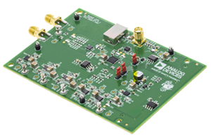
AD9789-EBZ

Part Number : AD9789-EBZ

Analog Devices Inc.
The AD9789 is a flexible QAM encoder/interpolator/upconverter combined with a high performance, 2400 MSPS, 14-bit RF digital-to-analog converter (DAC). The flexible digital interface can accept up to four channels of complex data. The QAM encoder supports constellation sizes of 16, 32, 64, 128, and 256 with SRRC filter coefficients for all standards.The on-chip rate converter supports a wide range of baud rates with a fixed DAC clock. The digital upconverter can place the channels from 0 to 0.5 × fDAC. This permits four contiguous channels to be synthesized and placed anywhere from dc to fDAC.The AD9789 includes a serial peripheral interface (SPI) for device configuration and status register readback. The flexible digital interface can be configured for data bus widths of 4, 8, 16, and 32 bits. It can accept real or complex data.The AD9789 operates from 1.5 V, 1.8 V, and 3.3 V supplies for a total power consumption of 1.6 W. It is supplied in a 164-ball chip scale package ball grid array for lower thermal impedance and reduced package parasitics. No special power sequencing is required. The clock receiver powers up muted to prevent start-up noise.Product Highlights Highly integrated and configurable QAM mappers, interpolators, and upconverters for direct synthesis of one to four DOCSIS- or DVB-C-compatible channels in a block. Low noise and intermodulation distortion (IMD) performance enable high quality synthesis of signals up to 1 GHz. Flexible data interface supports LVDS for improved SFDR or CMOS input data for less demanding applications. Interface is configurable from 4-bit nibbles to 32-bit words and can run at up to 150 MHz CMOS or 150 MHz LVDS double data rate (DDR). Manufactured on a CMOS process, the AD9789 uses a proprietary switching technique that enhances dynamic performance.Applications Broadband communications systems CMTS/DVB Cellular infrastructure Point-to-point wireless

ADA4505-1ARJZ-R7

Part Number : ADA4505-1ARJZ-R7

Analog Devices Inc.
The ADA4505-1/ADA4505-2/ADA4505-4 are single, dual, and quad micropower amplifiers featuring rail-to-rail input and output swings while operating from a single 1.8 V to 5 V power supply or from dual ±0.9 V to ±2.5 V power supplies.Employing a new circuit technology, these low cost amplifiers offer zero input crossover distortion (excellent PSRR and CMRR performance) and very low bias current, while operating with a supply current of less than 10 μA per amplifier.This combination of features makes the ADA4505-x amplifiers ideal choices for battery-powered applications because they minimize errors due to power supply voltage variations over the lifetime of the battery and maintain high CMRR even for a rail-to-rail op amp.Remote battery-powered sensors, handheld instrumentation and consumer equipment, hazard detectors (for example, smoke, fire, and gas), and patient monitors can benefit from the features of the ADA4505-x amplifiers.The ADA4505-x family is specified for both the industrial temperature range (−40°C to +85°C) and the extended industrial temperature range (−40°C to +125°C). The ADA4505-1 single amplifier is available in a tiny 5-lead SOT-23. The ADA4505-2 dual amplifier is available in a standard 8-lead MSOP and a 8-ball WLCSP. The ADA4505-4 quad amplifier is available in a 14-lead TSSOP and a 14-ball WLCSP.The ADA4505-x family is a member of a growing series of zero crossover op amps offered by Analog Devices, Inc., including the AD8506/AD8508, which also operate from a single 1.8 V to 5 V power supply or from dual ±0.9 V to ±2.5 V power supplies.ApplicationsPressure and position sensorsRemote securityMedical monitorsBattery-powered consumer equipmentHazard detectors

ADA4528-1ARMZ

Part Number : ADA4528-1ARMZ

Analog Devices Inc.
The ADA4528-1/ADA4528-2 are ultralow noise, zero-drift operational amplifiers featuring rail-to-rail input and output swing. With an offset voltage of 2.5 μV, offset voltage drift of 0.015 μV/°C, and typical noise of 97 nV p-p (0.1 Hz to 10 Hz, AV = +100), the ADA4528-1/ADA4528-2 are well suited for applications in which error sources cannot be tolerated.The ADA4528-1/ADA4528-2 have a wide operating supply range of 2.2 V to 5.5 V, high gain, and excellent CMRR and PSRR specifications, which make it ideal for applications that require precision amplification of low level signals, such as position and pressure sensors, strain gages, and medical instrumentation.The ADA4528-1/ADA4528-2 are specified over the extended industrial temperature range (−40°C to +125°C). The ADA4528-1 and ADA4528-2 are available in 8-lead MSOP and 8-lead LFCSP packages.For more information about the ADA4528-1/ADA4528-2, see the AN-1114 Application Note, Lowest Noise Zero-Drift Amplifier Has 5.6 nV/√Hz Voltage Noise Density.Applications Thermocouple/thermopile Load cell and bridge transducers Precision instrumentation Electronic scales Medical instrumentation Handheld test equipment

ADA4610-2ARZ

Part Number : ADA4610-2ARZ

Analog Devices Inc.
The ADA4610-1/ADA4610-2/ADA4610-4 are precision junction field effect transistor (JFET) amplifiers that feature low input noise voltage, current noise, offset voltage, input bias current, and rail-to-rail output. The ADA4610-1 is a single amplifier, the ADA4610-2 is a dual amplifier, and the ADA4610-4 is a quad amplifier.The combination of low offset, noise, and very low input bias current makes these amplifiers especially suitable for high impedance sensor amplification and precise current measurements using shunts. With excellent dc precision, low noise, and fast settling time, the ADA4610-1/ADA4610-2/ADA4610-4 provide superior accuracy in medical instruments, electronic measurement, and automated test equipment. Unlike many competitive amplifiers, the ADA4610-1/ADA4610-2/ADA4610-4 maintain fast settling performance with substantial capacitive loads. Unlike many older JFET amplifiers, the ADA4610-1/ADA4610-2/ADA4610-4 do not suffer from output phase reversal when input voltages exceed the maximum common-mode voltage range. The fast slew rate and great stability with capacitive loads make the ADA4610-1/ADA4610-2/ADA4610-4 ideal for high performance filters. Low input bias currents, low offset, and low noise result in a wide dynamic range for photodiode amplifier circuits. Low noise and distortion, high output current, and excellent speed make the ADA4610-1/ADA4610-2/ ADA4610-4 great choices for audio applications.The ADA4610-1/ADA4610-2/ADA4610-4 are specified over the −40°C to +125°C extended industrial temperature range.The ADA4610-1 is available in an 8-lead SOIC package and in a 5-lead SOT-23 package. The ADA4610-2 is available in 8-lead SOIC, 8-lead MSOP, and 8-lead LFCSP packages. The ADA4610-4 is available in a 14-lead SOIC package and in a 16-lead LFCSP.Applications Instrumentation Medical instruments Multipole filters Precision current measurement Photodiode amplifiers Sensors Audio

ADA4610-2BRZ

Part Number : ADA4610-2BRZ

Analog Devices Inc.
The ADA4610-1/ADA4610-2/ADA4610-4 are precision junction field effect transistor (JFET) amplifiers that feature low input noise voltage, current noise, offset voltage, input bias current, and rail-to-rail output. The ADA4610-1 is a single amplifier, the ADA4610-2 is a dual amplifier, and the ADA4610-4 is a quad amplifier.The combination of low offset, noise, and very low input bias current makes these amplifiers especially suitable for high impedance sensor amplification and precise current measurements using shunts. With excellent dc precision, low noise, and fast settling time, the ADA4610-1/ADA4610-2/ADA4610-4 provide superior accuracy in medical instruments, electronic measurement, and automated test equipment. Unlike many competitive amplifiers, the ADA4610-1/ADA4610-2/ADA4610-4 maintain fast settling performance with substantial capacitive loads. Unlike many older JFET amplifiers, the ADA4610-1/ADA4610-2/ADA4610-4 do not suffer from output phase reversal when input voltages exceed the maximum common-mode voltage range. The fast slew rate and great stability with capacitive loads make the ADA4610-1/ADA4610-2/ADA4610-4 ideal for high performance filters. Low input bias currents, low offset, and low noise result in a wide dynamic range for photodiode amplifier circuits. Low noise and distortion, high output current, and excellent speed make the ADA4610-1/ADA4610-2/ ADA4610-4 great choices for audio applications.The ADA4610-1/ADA4610-2/ADA4610-4 are specified over the −40°C to +125°C extended industrial temperature range.The ADA4610-1 is available in an 8-lead SOIC package and in a 5-lead SOT-23 package. The ADA4610-2 is available in 8-lead SOIC, 8-lead MSOP, and 8-lead LFCSP packages. The ADA4610-4 is available in a 14-lead SOIC package and in a 16-lead LFCSP.Applications Instrumentation Medical instruments Multipole filters Precision current measurement Photodiode amplifiers Sensors Audio

ADA4800ACPZ-RL

Part Number : ADA4800ACPZ-RL

Analog Devices Inc.
The ADA4800 is a voltage buffer amplifier integrated with an active load. The buffer is a low power, high speed, low noise, high slew rate, fast settling, fixed gain of 1 monolithic amplifier for charge-coupled device (CCD) applications. For CCD applications, the active load current source (IAL) can load the open source CCD sensor outputs and the buffer can drive the AFE load. The active current load can also be switched off, to use the ADA4800 as just a unity gain buffer. The buffer consumes only 20 mW of static power. In applications where power savings is critical, the ADA4800 features a power save mode (see the Power Save Mode section), which further reduces the total current consumption. The bandwidth of the ADA4800 buffer is also fully adjustable through the IDRV pin.The buffer of the ADA4800 employs a push-pull output stage architecture, providing drive current and maximum slew capability for both rising and falling signal transitions. At a 5 mA quiescent current setting, it provides 400 MHz, −3 dB bandwidth, which makes this buffer well suited for CCD sensors from machine vision to digital still camera applications.The ADA4800 is ideal for driving the input of the Analog Devices, Inc., 12-bit and 14-bit high resolution analog front ends (AFE) such as the AD9928, AD9990, AD9920A, AD9923A, and AD997x family.The versatility of the ADA4800 allows for seamless interfacing with many CCD sensors from various manufacturers.The ADA4800 is designed to operate at supply voltages as low as 4 V and up to 17 V. It is available in a 1.6 mm × 1.6 mm × 0.55 mm, 6-lead LFCSP package and is rated to operate over the industrial temperature range of −40°C to +85°C.Applications CCD image sensor output buffer Digital still cameras Camcorders

ADA4891-1ARJZ-RL

Part Number : ADA4891-1ARJZ-RL

Analog Devices Inc.
The ADA4891-1 (single), ADA4891-2 (dual), ADA4891-3 (triple), and ADA4891-4 (quad) are CMOS, high speed amplifiers that offer high performance at a low cost. The amplifiers feature true single-supply capability, with an input voltage range that extends 300 mV below the negative rail. In spite of their low cost, the ADA4891 family provides high performance and versatility. The rail-to-rail output stage enables the output to swing within 50 mV of each rail, enabling maximum dynamic range. The ADA4891 family of amplifiers is ideal for imaging applications, such as consumer video, CCD buffers, and contact image sensor buffers. Low distortion and fast settling time also make them ideal for active filter applications. The ADA4891-1/ADA4891-2/ADA4891-3/ADA4891-4 are available in a wide variety of packages. The ADA4891-1 is available in 8-lead SOIC and 5-lead SOT-23 packages. The ADA4891-2 is available in 8-lead SOIC and 8-lead MSOP packages. The ADA4891-3 and ADA4891-4 are available in 14-lead SOIC and 14-lead TSSOP packages. The amplifiers are specified to operate over the extended temperature range of −40°C to +125°C.Applications Imaging Consumer video Active filters Coaxial cable drivers Clock buffers Photodiode preamp Contact image sensor and buffers

Displaying 381 - 400 of 93399

Latest Parts

SC1112

Raspberry Pi

$79.61 - $86.40

IN STOCK 10275
Buy

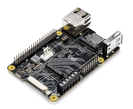
ASX00049

Arduino

* $39.41 - * $44.41

IN STOCK 3132
Buy

AD96685BRZ

Analog Devices Inc.

$1.72 - * $11.79

IN STOCK 4921
Buy

Reference Designs

RD006

Wurth Elektronik

RD006 - 3 W Dual-output isolated auxiliary supply for communication interfaces and measurement systems

CN0583

Analog Devices Inc.

Multistandard Micropower Verified Smoke Detection System-on-Module

Technical Resources

EVALUATION KITS

EVAL-AD7124-8SDZ

Analog Devices Inc.

$71.02 - * $75.98

IN STOCK 808
Buy
View All