AD8475BRMZ
Part Number : AD8475BRMZ
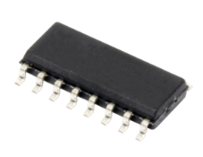
Analog Devices Inc.The AD8475 is a fully differential, attenuating amplifier with integrated precision gain resistors. It provides precision attenuation (by 0.4 or 0.8), common-mode level shifting, and single-ended-to-differential conversion along with input overvoltage protection. Power dissipation on a single 5 V supply is only 16 mW.The AD8475 is a simple to use, fully integrated precision gain block, designed to process signal levels of up to ±10 V on a single supply. It provides a complete interface to make industrial level signals directly compatible with the differential input ranges of low voltage high performance 16-bit or 18-bit single-supply successive approximation (SAR) analog-to-digital converters (ADCs).The AD8475 comes with two standard pin-selectable gain options: 0.4 and 0.8. The gain of the part is set by driving the input pin corresponding to the appropriate gain.The AD8475 also provides overvoltage protection from large industrial input voltages up to ±15 V while operating on a single 5 V supply. The VOCM pin adjusts the output voltage common mode for precision level shifting, to match the ADC’s input range and maximize dynamic range.The AD8475 works extremely well with SAR, Σ-Δ, and pipeline converters. The high current output stage of the part allows it to drive the switched capacitor front-end circuits of many ADCs with minimal error.Unlike many differential drivers in the market, the AD8475 is a high precision amplifier. With 500 μV maximum output offset, 10 nV/√Hz output noise, and −112 dB THD + N, the AD8475 pairs well with high accuracy converters. Considering its low power consumption and high precision, the slew-enhanced AD8475 has excellent speed, settling to 18-bit precision for 4 MSPS acquisition.The AD8475 is available in a space-saving 16-lead 3 mm × 3 mm LFCSP package and a 10-lead MSOP package. It is fully specified over the −40°C to +85°C temperature range.Applications ADC drivers Differential instrumentation amplifier building blocks Single-ended-to-differential converters
AD8657ARMZ
Part Number : AD8657ARMZ
Analog Devices Inc.The AD8657/AD8659 are dual and quad micropower, precision,rail-to-rail input/output amplifiers optimized for low power and wide operating supply voltage range applications.The AD8657/AD8659 operate from 2.7 V to 18 V with a typicalquiescent supply current of 18 μA. The devices use the AnalogDevices, Inc., patented DigiTrim® trimming technique, whichachieves low offset voltage. The AD8657/AD8659 also have high immunity to electromagnetic interference.The combination of low supply current, low offset voltage, very low input bias current, wide supply range, and rail-to-rail input and output make the AD8657/AD8659 ideal for currentmonitoring in process and motor control applications. Thecombination of precision specifications makes these devicesideal for dc gain and buffering of sensor front ends or high impedance input sources in wireless or remote sensors or transmitters.The AD8657/AD8659 are specified over the extended industrial temperature range (−40°C to +125°C). The AD8657 is available in an 8-lead MSOP package and an 8-lead LFCSP package; the AD8659 is available in a 14-lead SOIC package and 16-leadLFCSP package.Applications Portable operating systems Current monitors 4 mA to 20 mA loop drivers Buffer/level shifting Multipole filters Remote/wireless sensors Low power transimpedance amplifiers
AD9125BCPZRL
Part Number : AD9125BCPZRL
Analog Devices Inc.The AD9125 is a dual, 16-bit, high dynamic range TxDAC+® digital-to-analog converter (DAC) that provides a sample rate of 1000 MSPS, permitting a multicarrier generation up to the Nyquist frequency. It includes features optimized for direct conversion transmit applications, including complex digital modulation, and gain and offset compensation. The DAC outputs are optimized to interface seamlessly with analog quadrature modulators, such as the ADL537x F-MOD series from Analog Devices, Inc. A 4-wire serial port interface allows programming/readback of many internal parameters. Full-scale output current can be programmed over a range of 8.7 mA to 31.7 mA. The AD9125 comes in a 72-lead LFCSP.PRODUCT HIGHLIGHTS Ultralow noise and intermodulation distortion (IMD) enable high quality synthesis of wideband signals from baseband to high intermediate frequencies. A proprietary DAC output switching technique enhances dynamic performance. The current outputs are easily configured for various single-ended or differential circuit topologies. Flexible CMOS digital interface allows the standard 32-wire bus to be reduced to a 16-wire bus.APPLICATIONS Wireless infrastructure W-CDMA, CDMA2000, TD-SCDMA, WiMAX, GSM, LTE Digital high or low IF synthesis Transmit diversity Wideband communications: LMDS/MMDS, point-to-point Cable modem termination systems
AD8226BRZ
Part Number : AD8226BRZ
Analog Devices Inc.The AD8226 is a low cost, wide supply range instrumentation amplifier that requires only one external resistor to set any gain between 1 and 1000.The AD8226 is designed to work with a variety of signal voltages. A wide input range and rail-to-rail output allow the signal to make full use of the supply rails. Because the input range also includes the ability to go below the negative supply, small signals near ground can be amplified without requiring dual supplies. The AD8226 operates on supplies ranging from ±1.35 V to ±18 V for dual supplies and 2.2 V to 36 V for single supply.The robust AD8226 inputs are designed to connect to real-world sensors. In addition to its wide operating range, the AD8226 can handle voltages beyond the rails. For example, with a ±5 V supply, the part is guaranteed to withstand ±35 V at the input with no damage. Minimum as well as maximum input bias currents are specified to facilitate open wire detection.The AD8226 is perfect for multichannel, space-constrained industrial applications. Unlike other low cost, low power instrumentation amplifiers, the AD8226 is designed with a minimum gain of 1 and can easily handle ±10 V signals. With its MSOP package and 125°C temperature rating, the AD8226 thrives in tightly packed, zero airflow designs.The AD8226 is available in 8-lead MSOP and SOIC packages, and is fully specified for −40°C to +125°C operation.For a device with a similar package and performance as the AD8226 but with gain settable from 5 to 1000, consider using the AD8227.ApplicationsIndustrial process controlsBridge amplifiersMedical instrumentationPortable data acquisitionMultichannel systems
AD8622ARZ
Part Number : AD8622ARZ
Analog Devices Inc.The AD8622 is a dual, precision rail-to-rail output operational amplifier with a low supply current of only 350 μA maximum over temperature and supply voltages. It also offers ultralow offset, drift, and voltage noise combined with very low input bias current over the full operating temperature range.With typical offset voltage of only 10 μV, offset drift of 0.5 μV/°C, and noise of only 0.2 μV p-p (0.1 Hz to 10 Hz), it is perfectly suited for applications where large error sources cannot be tolerated. Many systems can take advantage of the low noise, dc precision, and rail-to-rail output swing provided by the AD8622 to maximize the signal-to-noise ratio and dynamic range for low power operation. The AD8622 is specified for the extended industrial temperature range of −40°C to +125°C and is available in lead-free SOIC and MSOP packages.ApplicationsPortable precision instrumentationLaser diode control loopsMedical InstrumentationStrain gage amplifiersThermocouple amplifiers
AD8665ARZ-REEL
Part Number : AD8665ARZ-REEL
Analog Devices Inc.The AD866x family are single supply, rail-to-rail output amplifiers with low noise performance featuring an extended operating range with supply voltages up to 16 V. They also feature low input bias currents, wide signal bandwidth, and low input voltage and current noise. For lower offset voltage, choose the AD8661/AD8662/AD8664 family.The combination of low offset, very low input bias current, and a wide supply range makes these amplifiers useful in a wide variety of applications usually associated with higher priced JFET amplifiers. Systems using high impedance sensors, such as photodiodes, benefit from the combination of low input bias current, low noise, low offset, and wide bandwidth. The wide operating voltage range matches high performance ADCs and DACs. Audio applications and medical monitoring equipment can take advantage of the high input impedance, low voltage and current noise, wide bandwidth, and the lack of popcorn noise found in many other low input bias current amplifiers.The AD866x family is specified over the extended industrial temperature range (−40°C to +125°C). ApplicationsReference Buffers Medical Equipment Physiological measurementsSignal filters and conditioning Consumer audio Photodiode amplificationADC driver Level shifting circuits Data Sheet, Rev. A, 10/06
AD9219ABCPZ-65
Part Number : AD9219ABCPZ-65
Analog Devices Inc.The AD9219 is a quad, 10-bit, 40/65 MSPS analog-to-digital con-verter (ADC) with an on-chip sample-and-hold circuit designedfor low cost, low power, small size, and ease of use. The productoperates at a conversion rate of up to 65 MSPS and is optimized foroutstanding dynamic performance and low power in applications where a small package size is critical.The ADC requires a single 1.8 V power supply and LVPECL-/ CMOS-/LVDS-compatible sample rate clock for full performanceoperation. No external reference or driver components arerequired for many applications.The ADC automatically multiplies the sample rate clock for theappropriate LVDS serial data rate. A data clock output (DCO) for capturing data on the output and a frame clock output (FCO) for signaling a new output byte are provided. Individual-channel power-down is supported and typically consumes less than 2 mW when all channels are disabled.The ADC contains several features designed to maximizeflexibility and minimize system cost, such as programmableclock and data alignment and programmable digital test patterngeneration. The available digital test patterns include built-in deterministic and pseudorandom patterns, along with custom user- defined test patterns entered via the serial port interface (SPI).The AD9219 is available in an RoHS compliant, 48-lead LFCSP. It is specified over the industrial temperature range of −40°C to +85°C.Product Highlights Small Footprint. Four ADCs are contained in a small, space-saving package. Low power of 94 mW/channel at 65 MSPS. Ease of Use. A data clock output (DCO) is provided that operates at frequencies of up to 390 MHz and supports double data rate (DDR) operation. User Flexibility. The SPI control offers a wide range of flexible features to meet specific system requirements. Pin-Compatible Family. This includes the AD9287 (8-bit), AD9228 (12-bit), and AD9259 (14-bit). ApplicationsMedical imaging and nondestructive ultrasoundPortable ultrasound and digital beam-forming systemsQuadrature radio receiversDiversity radio receiversTape drivesOptical networkingTest equipment
AD9522-3/PCBZ
Part Number : AD9522-3/PCBZ
Analog Devices Inc.The AD9522-31 provides a multioutput clock distribution function with subpicosecond jitter performance, along with an on-chip PLL and VCO. The on-chip VCO tunes from 1.72 GHz to 2.25 GHz. An external 3.3 V/5 V VCO/VCXO of up to 2.4 GHz can also be used. The AD9522 serial interface supports both SPI and I2C® ports. An in-package EEPROM can be programmed through the serial interface and store user-defined register settings for power-up and chip reset.The AD9522 features 12 LVDS outputs in four groups. Any of the 800 MHz LVDS outputs can be reconfigured as two 250 MHz CMOS outputs.Each group of outputs has a divider that allows both the divide ratio (from 1 to 32) and the phase (coarse delay) to be set. The AD9522 is available in a 64-lead LFCSP and can be operated from a single 3.3 V supply. The external VCO can have an operating voltage up to 5.5 V. The AD9522 is specified for operation over the standard industrialrange of −40°C to +85°C.The AD9520-3 is an equivalent part to the AD9522-3 featuringLVPECL / CMOS drivers instead of LVDS / CMOS drivers.1The AD9522 is used throughout this data sheet to refer to all the members of the AD9522 family. However, when AD9522-3 is used, it is referring to that specificmember of the AD9522 family.ApplicationsLow jitter, low phase noise clock distributionClock generation and translation for SONET, 10Ge, 10G FC, and other 10 Gbps protocolsForward error correction (G.710)Clocking high speed ADCs, DACs, DDSs, DDCs, DUCs, MxFEsHigh performance wireless transceiversATE and high performance instrumentationBroadband infrastructuresData Sheet, Rev. 0, 10/08
ADA4857-1YRZ
Part Number : ADA4857-1YRZ
Analog Devices Inc.The ADA4857 is a unity gain stable, high speed, voltage feedback amplifier with low distortion, low noise, and high slew rate. With a spurious-free dynamic range (SFDR) of −88 dBc @ 10 MHz, the ADA4857 is an ideal solution for a variety of applications including ultrasounds, ATE, active filters, and ADC drivers. The Analog Devices, Inc., proprietary next-generation XFCB process and innovative architecture enables such high performance amplifiers. The ADA4857 has 850 MHz bandwidth, 2800 V/μs slew rate, and settles to 0.1% in 15 ns. With a wide supply voltage range (5 V to 10 V), the ADA4857 is an ideal candidate for systems that require high dynamic range, precision, and speed. The ADA4857-1 amplifier is available in a 3 mm × 3 mm, 8-lead LFCSP and a standard 8-lead SOIC. The ADA4857-2 is available in a 4 mm × 4 mm, 16-lead LFSCP. The LFCSP features an exposed paddle that provides a low thermal resistance path to the printed circuit board (PCB). This path enables more efficient heat transfer and increases reliability. The ADA4857 works over the extended industrial temperature range (−40°C to +125°C). ApplicationsInstrumentationIF and baseband amplifiersActive filtersADC driversDAC bufferstable.nopad td, table.nopad th { padding: 0px; margin: 0px; vertical-align: top;}
ADG1407BRUZ
Part Number : ADG1407BRUZ
Analog Devices Inc.The ADG1406 and ADG1407 are monolithic iCMOS® analogmultiplexers comprising 16 single channels and eight differentialchannels, respectively. The ADG1406 switches one of 16 inputsto a common output, as determined by the 4-bit binary addresslines (A0, A1, A2, and A3). The ADG1407 switches one of eightdifferential inputs to a common differential output, as determinedby the 3-bit binary address lines (A0, A1, and A2). An EN inputon both devices enables or disables the device. When disabled,all channels switch off. When on, each channel conducts equallywell in both directions and has an input signal range that extendsto the supplies.The iCMOS (industrial CMOS) modular manufacturingprocess combines high voltage CMOS (complementary metaloxidesemiconductor) and bipolar technologies. It enables thedevelopment of a wide range of high performance analog ICscapable of 33 V operation in a footprint that no other generationof high voltage parts has been able to achieve. Unlike analog ICsusing conventional CMOS processes, iCMOS components cantolerate high supply voltages while providing increased performance,dramatically lower power consumption, and reducedpackage size.The ultralow on resistance and on-resistance flatness of theseswitches make them ideal solutions for data acquisition andgain switching applications where low distortion is critical.iCMOS construction ensures ultralow power dissipation,making the parts ideally suited for portable and battery-poweredinstruments. Applications Medical equipment Audio and video routing Automatic test equipment Data acquisition systems Battery-powered systems Sample-and-hold systems Communication systems
ADIS16060BCCZ
Part Number : ADIS16060BCCZ
Analog Devices Inc.The ADIS16060 is a yaw rate gyroscope with an integrated serial peripheral interface (SPI). It features an externally selectable bandwidth response and scalable dynamic range.The SPI port provides access to the rate sensor, an internal temperature sensor, and two external analog signals (using internal ADC). The digital data available at the SPI port is proportional to the angular rate about the axis that is normal to the top surface of the package.An additional output pin provides a precision voltage reference. A digital self-test function electromechanically excites the sensor to test the operation of the sensor and the signal-conditioning circuits.The ADIS16060 is available in an 8.2 mm × 8.2 mm × 5.2 mm, 16-terminal, peripheral land grid array (LGA) package.APPLICATIONS Platform stabilization Image stabilization Guidance and control Inertial measurement units Robotics
ADIS16209CCCZ
Part Number : ADIS16209CCCZ
Analog Devices Inc.The ADIS16209 is a high accuracy, digital inclinometer that accommodates both single-axis (±180°) and dual-axis (±90°) operation. The standard supply voltage (3.3 V) and serial peripheral interface (SPI) enable simple integration into most industrial system designs. A simple internal register structure handles all output data and configuration features. This includes access to the following output data: calibrated acceleration, accurate incline angles, power supply, internal temperature, auxiliary analog and digital input signals, diagnostic error flags, and programmable alarm conditions.Configurable operating parameters include sample rate, power management, digital filtering, auxiliary analog and digital output, offset/null adjustment, and self-test for sensor mechanical structure.The ADIS16209 is available in a 9.2 mm × 9.2 mm × 3.9 mm LGA package that operates over a temperature range of −40°C to +125°C. It can be attached using standard RoHS-compliant solder reflow processes.APPLICATIONS Platform control, stabilization, and alignment Tilt sensing, inclinometers, leveling Motion/position measurement Monitor/alarm devices (security, medical, safety) Navigation
ADL5356ACPZ-R7
Part Number : ADL5356ACPZ-R7
Analog Devices Inc.The ADL5356 uses a highly linear, doubly balanced, passive mixer core along with integrated RF and local oscillator (LO) balancing circuitry to allow single-ended operation. The ADL5356 incorporates the RF baluns, allowing for optimal performance over a 1200 MHz to 2500 MHz RF input frequency range. Performance is optimized for RF frequencies from 1700 MHz to 2500 MHz using a low-side LO and RF frequencies from 1200 MHz to 1700 MHz using a high-side LO. The balanced passive mixer arrangement provides good LO-to-RF leakage, typically better than −35 dBm, and excellent intermodulation performance. The balanced mixer core also provides extremely high input linearity, allowing the device to be used in demanding cellular applications where in-band blocking signals may otherwise result in the degradation of dynamic performance. A high linearity IF buffer amplifier follows the passive mixer core to yield a typical power conversion gain of 8.2 dB and can be used with a wide range of output impedances.The ADL5356 provides two switched LO paths that can be used in TDD applications where it is desirable to ping-pong between two local oscillators. LO current can be externally set using a resistor to minimize dc current commensurate with the desired level of performance. For low voltage applications, the ADL5356 is capable of operation at voltages down to 3.3 V with substantially reduced current. Under low voltage operation, an additional logic pin is provided to power down (
ADXL312ACPZ
Part Number : ADXL312ACPZ
Analog Devices Inc.The ADXL312 is a small, thin, low power, 3-axis accelerometer with high resolution (13-bit) measurement up to ±12 g. Digital output data is formatted as 16-bit twos complement and is accessible through either a serial port interface (SPI) (3- or 4-wire) or I2C digital interface.The ADXL312 is well suited for car alarm or black box applications. It measures the static acceleration of gravity in tilt-sensing applications, as well as dynamic acceleration resulting from motion or shock. Its high resolution (2.9 mg/LSB) enables resolution of inclination changes of as little as 0.25°. A built-in FIFO facilitates using oversampling techniques to improve resolution to as little as 0.05° of inclination.Several special sensing functions are provided. Activity and inactivity sensing detects the presence or absence of motion and whether the acceleration on any axis exceeds a user-set level. These functions can be mapped to interrupt output pins. An integrated 32 level FIFO can be used to store data to minimize host processor intervention.Low power modes enable intelligent motion-based power management with threshold sensing and active acceleration measurement at extremely low power dissipation.The ADXL312 is supplied in a small, thin 5 mm × 5 mm × 1.45 mm, 32-lead, LFCSP package.APPLICATIONS Car alarm Hill start aid (HSA) Electronic parking brake Data recorder (black box)
ADXRS620BBGZ
Part Number : ADXRS620BBGZ
Analog Devices Inc.The ADXRS620 is a complete angular rate sensor (gyroscope)that uses the Analog Devices, Inc. surface-micromachiningprocess to create a functionally complete and low cost angularrate sensor integrated with all required electronics on one chip.The manufacturing technique for this device is the same highvolume BiMOS process used for high reliability automotiveairbag accelerometers.The ADXRS620 is an automotive grade gyroscope that has 100% pin, package, temperature, and function compatible to the available industrial grade ADXRS652 gyro. Automotive grade gyroscopes have more extensive guaranteed min/max specifications due to automotive testing.The output signal, RATEOUT (1B, 2A), is a voltageproportional to angular rate about the axis normal to the topsurface of the package. The output is ratiometric with respect toa provided reference supply. A single external resistor can beused to lower the scale factor. An external capacitor sets thebandwidth. Other external capacitors are required for operation.A temperature output is provided for compensation techniques.Two digital self-test inputs electromechanically excite thesensor to test proper operation of both the sensor and the signalconditioning circuits. The ADXRS620 is available in a 7 mm ×7 mm × 3 mm BGA ceramic package.APPLICATIONS Vehicle chassis rollover sensing Inertial measurement units Platform stabilization
ADXRS652BBGZ
Part Number : ADXRS652BBGZ
Analog Devices Inc.The ADXRS652 is a complete angular rate sensor (gyroscope) that uses the Analog Devices, Inc. surface-micromachining process to make a functionally complete and low cost angular rate sensor integrated with all of the required electronics on one chip. The manufacturing technique for this device is a patented high volume BIMOS process with years of proven field reliability.The ADXRS652 is an industrial grade gyroscope that 100% pin, package, temperature, and function compatible to the related automotive grade ADXRS620 and ADXRS622 gyroscopes. Automotive grade gyroscopes have more guaranteed min/max specifications due to automotive testing.The output signal, RATEOUT (1B, 2A), is a voltage proportional to angular rate about the axis normal to the top surface of the package. The output is ratiometric with respect to a provided reference supply. An external capacitor is used to set the bandwidth. Other external capacitors are required for operation.A temperature output is provided for compensation techniques. Two digital self-test inputs electromechanically excite the sensor to test proper operation of both the sensor and the signal conditioning circuits. The ADXRS652 is available in a 7 mm × 7 mm × 3 mm BGA chip-scale package.
DC1370A-N
Part Number : DC1370A-N
Analog Devices Inc.The LTC2262-12 is a sampling 12-bit A/D converter designed for digitizing high frequency, wide dynamic range signals. The LTC2262-12 is perfect for demanding communications applications with AC performance that includes 70.5dB SNR and 88dB spurious free dynamic range (SFDR). Ultralow jitter of 0.17psRMS allows undersampling of IF frequencies with excellent noise performance.DC specs include ±0.3LSB INL (typical), ±0.1LSB DNL (typical) and no missing codes over temperature. The transition noise is a low 0.3LSBRMS.The digital outputs can be either full rate CMOS, double data rate CMOS, or double data rate LVDS. A separate output power supply allows the CMOS output swing to range from 1.2V to 1.8V.The ENC+ and ENC– inputs may be driven differentially or single-ended with a sine wave, PECL, LVDS, TTL or CMOS inputs. An optional clock duty cycle stabilizer allows high performance at full speed for a wide range of clock duty cycles. Bits LTC2262-12 12 LTC2262-14 14 Applications Communications Cellular Base Stations Software Defined Radios Portable Medical Imaging Multi-Channel Data Acquisition Nondestructive Testing
DC1398A-GA
Part Number : DC1398A-GA
Analog Devices Inc.The LTM9001 is an integrated System in a Package (SiP) that includes a high-speed 16-bit A/D converter, matching network, anti-aliasing filter and a low noise, differential amplifier with fixed gain. It is designed for digitizing wide dynamic range signals with an intermediate frequency (IF) range up to 300MHz. The amplifier allows either AC- or DC-coupled input drive. A lowpass or bandpass filter network can be implemented with various bandwidths. Contact Analog Devices regarding semi-custom configurations. The LTM9001 is perfect for IF receivers in demanding communications applications, with AC performance that includes 78dBFS noise floor and 87dB spurious free dynamic range (SFDR) at 5MHz (LTM9001-GA). The digital outputs are single-ended CMOS. A separate output power supply allows the CMOS output swing to range from 0.5V to 3.3V.An optional clock duty cycle stabilizer allows high performance at full speed with a wide range of clock duty cycles.Applications Telecommunications High Sensitivity Receivers Imaging Systems Spectrum Analyzers ATE
DC1449A
Part Number : DC1449A
Analog Devices Inc.The LT8415 is an ultralow power boost converter with two integrated complementary MOSFET half-bridges (N- and P-channel), integrated power switch, Schottky diode and output disconnect circuitry. The N-channel and P-channel MOSFETs in each half-bridge are synchronously controlled by a single input pin, and never turn on at the same time in typical applications.The boost regulator controls power delivery by varying both the peak inductor current and switch off-time. This control scheme results in low output voltage ripple as well as high efficiency over a wide load range. The quiescent current is a low 10.5μA, which is further reduced to 0μA in shutdown. The internal disconnect circuitry allows the output voltage to be blocked from the input during shutdown. High value (12.4M/0.4M) resistors are integrated on chip for output voltage detection, significantly reducing input referred quiescent current. The LT8415 also features a comparator built into the SHDN pin, overvoltage protection for the CAP, VOUT, OUT1 and OUT2 pins, built in soft start and comes in a tiny 12-pin 3mm × 2mm DFN package.Applications Sensor Power RF Mems Relay Power Low Power Actuator Bias/Control Liquid Lens Driver
DC1453A
Part Number : DC1453A
Analog Devices Inc.The LTM4619 is a complete dual 4A or single 8A stepdown DC/DC μModule® (power module) regulator. Included in the package are the switching controller, power FETs, inductor, and all support components. Operating over input voltage ranges of 4.5V to 26.5V, the LTM4619 supports two outputs with voltage ranges of 0.8V to 5V, each set by a single external resistor. Its high efficiency design delivers 4A continuous current (5A peak) for each output.High switching frequency and a current mode architecture enable a very fast transient response to line and load changes without sacrificing stability. The two outputs are interleaved with 180° phase to minimize the ripple noise and reduce the I/O capacitors. The device supports frequency synchronization and output voltage tracking for supply rail sequencing. Burst Mode operation or pulseskipping mode can be selected for light load operations.Fault protection features include overvoltage protection, overcurrent protection and foldback current limit for short-circuit protection.The low profile package (2.82mm) enables utilization of unused space on the bottom of PC boards for high density point of load regulation. The power module is offered in a 15mm × 15mm × 2.82mm LGA package. The LTM4619 is RoHS compliant with Pb-free finish.Applications Telecom and Networking Equipment Servers Storage Cards ATCA Cards Industrial Equipment Point of Load Regulation


