
OP4177ARZ
Part Number : OP4177ARZ
Analog Devices Inc.The OPx177 family consists of very high precision, single, dual, and quad amplifiers featuring extremely low offset voltage and drift, low input bias current, low noise, and low power consump-tion. Outputs are stable with capacitive loads of over 1000 pF with no external compensation. Supply current is less than 500 μA per amplifier at 30 V. Internal 500 Ω series resistors protect the inputs, allowing input signal levels several volts beyond either supply without phase reversal.Unlike previous high voltage amplifiers with very low offset voltages, the OP1177 (single) and OP2177 (dual) amplifiers are available in tiny 8-lead surface-mount MSOP and 8-lead narrow SOIC packages. The OP4177 (quad) is available in TSSOP and 14-lead narrow SOIC packages. Moreover, specified performance in the MSOP and the TSSOP is identical to performance in the SOIC package. MSOP and TSSOP are available in tape and reel only.The OPx177 family offers the widest specified temperature range of any high precision amplifier in surface-mount packaging. All versions are fully specified for operation from −40°C to +125°C for the most demanding operating environments.Applications for these amplifiers include precision diode power measurement, voltage and current level setting, and level detection in optical and wireless transmission systems. Additional applications include line-powered and portable instrumentation and controls—thermocouple, RTD, strain-bridge, and other sensor signal conditioning—and precision filters.Applications Wireless base station control circuits Optical network control circuits Instrumentation Sensors and controls Thermocouples Resistor thermal detectors (RTDs) Strain bridges Shunt current measurements Precision filters

ADP3300ARTZ-3.3RL7
Part Number : ADP3300ARTZ-3.3RL7
Analog Devices Inc.The ADP3300 is a member of the ADP330x family of precisionlow dropout anyCAP® voltage regulators. The ADP3300stands out from conventional LDOs with a novel architectureand an enhanced process. Its patented design requires only a0.47 µF output capacitor for stability. This device is stable withany capacitor, regardless of its ESR (Equivalent Series Resistance)value, including ceramic types (MLCC) for space restricted applications.The ADP3300 achieves exceptional accuracy of ±0.8%at room temperature and ±1.4% overall accuracy over temperature, line and load regulations. The dropout voltage of theADP3300 is only 80 mV (typical) at 50 mA.The ADP3300 operates with a wide input voltage range from3.0 V to 12 V and delivers a load current in excess of 50 mA. Itfeatures an error flag that signals when the device is about tolose regulation or when the short circuit or thermal overloadprotection is activated. Other features include shutdown andoptional noise reduction capabilities. The ADP330x anyCAP®LDO family offers a wide range of output voltages and outputcurrent levels from 50 mA to 200 mA: ADP3301 (100 mA) ADP3303 (200 mA)APPLICATIONS Cellular Telephones Notebook, Palmtop Computers Battery Powered Systems PCMCIA Regulators Bar Code Scanners Camcorders, Cameras

DC572A
Part Number : DC572A
Analog Devices Inc.The LTC1588/LTC1589/LTC1592 are serial input 12-/14-/16-bit multiplying current output DACs that operates from a single 5V supply. These SoftSpan™ DACs can be software-programmed for either unipolar or bipolar mode through a 3-wire SPI interface. In either mode, the voltage output range can also be software-programmed. Two output ranges in unipolar mode and four output ranges in bipolar mode are available.INL and DNL are accurate to 1LSB over the industrial temperature range in both unipolar and bipolar modes. True 16-bit 4-quadrant multiplication is achieved with on-chip four quadrant multiplication resistors. The LTC1588/LTC1589/LTC1592 are available in a 16-lead SSOP package.These devices include an internal deglitcher circuit that reduces the glitch impulse to less than 2nV-s (typ).The asynchronous clear pin resets the LTC1588/LTC1589/ LTC1592 to 0V in unipolar or bipolar mode.Applications Process Control and Industrial Automation Precision Instrumentation Direct Digital Waveform Generation Software-Controlled Gain Adjustment Automatic Test Equipment


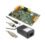
EVAL-ADV7181DEBZ
Part Number : EVAL-ADV7181DEBZ
Analog Devices Inc.Video IC Development Tools Evaluation Board I.C.

AD5220BRMZ10
Part Number : AD5220BRMZ10
Analog Devices Inc.The AD5220 provides a single channel, 128-position digitally controlled variable resistor (VR) device. This device performs the same electronic adjustment function as a potentiometer or variable resistor. These products were optimized for instrument and test equipment push-button applications. A choice between bandwidth or power dissipation are available as a result of the wide selection of end-to-end terminal resistance values.The AD5220 contains a fixed resistor with a wiper contact that taps the fixed resistor value at a point determined by a digitally controlled UP/DOWN counter. The resistance between the wiper and either end point of the fixed resistor provides a con stant resistance step size that is equal to the end-to-end resistance divided by the number of positions (e.g., RSTEP = 10 kΩ / 128 = 78Ω). The variable resistor offers a true adjustable value of resistance, between the A terminal and the wiper, or the B terminal and the wiper. The fixed A-to-B terminal resistance of 10 kΩ, 50 kΩ, or 100 kΩ has a nominal temperature coefficient of 800 ppm/°C.The chip select CS, count CLK and U/D direction control inputs set the variable resistor position. These inputs that control the internal UP/DOWN counter can be easily generated with mechanical or push button switches (or other contact closure devices). External debounce circuitry is required for the negative-edge sensitive CLK pin. This simple digital interface eliminates the need for microcontrollers in front panel interface designs.The AD5220 is available in both surface mount (SO-8) and the 8-lead plastic DIP package. For ultracompact solutions selected models are available in the thin μSOIC package. All parts are guaranteed to operate over the extended industrial temperature range of -40°C to +85°C. For 3-wire, SPI compatible interface applications, see the AD7376 / AD8400 / AD8402 / AD8403 products.APPLICATIONS Mechanical Potentiometer Replacement Remote Incremental Adjustment Applications Instrumentation: Gain, Offset Adjustment Programmable Voltage-to-Current Conversion Programmable Filters, Delays, Time Constants Line Impedance Matching Power Supply Adjustment

AD5241BRZ1M-REEL
Part Number : AD5241BRZ1M-REEL
Analog Devices Inc.The AD5241 / AD5242 provide a single-/dual-channel, 256-position, digitally controlled variable resistor (VR) device. These devices perform the same electronic adjustment function as a potentiometer, trimmer, or variable resistor. Each VR offers a completely programmable value of resistance between the A terminal and the wiper, or the B terminal and the wiper. For the AD5242, the fixed A-to-B terminal resistance of 10 kΩ, 100 kΩ, or 1 MΩ has a 1% channel-to-channel matching tolerance. The nominal temperature coefficient of both parts is 30 ppm/°C.Wiper position programming defaults to midscale at system power on. When powered, the VR wiper position is programmed by an I2C-compatible, 2-wire serial data interface. Both parts have two extra programmable logic outputs available that enable users to drive digital loads, logic gates, LED drivers, and analog switches in their system.The AD5241 / AD5242 are available in surface-mount, 14-lead SOIC and 16-lead SOIC packages and, for ultracompact solutions, 14-lead TSSOP and 16-lead TSSOP packages. All parts are guaranteed to operate over the extended temperature range of −40°C to +105°C.APPLICATIONS Multimedia, video, and audio Communications Mechanical potentiometer replacement Instrumentation: gain, offset adjustment Programmable voltage-to-current conversion Line impedance matching

AD5306ARUZ
Part Number : AD5306ARUZ
Analog Devices Inc.The AD5306 / AD5316 / AD5326 are quad 8-, 10-, and 12-bit buffered voltage output DACs, in a 16-lead TSSOP package, that operate from a single 2.5 V to 5.5 V supply, consuming 500 µA at 3 V. Their on-chip output amplifiers allow rail-to-rail output swing with a slew rate of 0.7 V/μs. A 2-wire serial interface that operates at clock rates up to 400 kHz is used. This interface is SMBus-compatible at VDD

AD5542ARZ
Part Number : AD5542ARZ
Analog Devices Inc.The AD5541 / AD5542 are single, 16-bit, serial input, voltage output digital-to-analog converters (DACs) that operate from a single 2.7 V to 5.5 V supply. The DAC output range extends from 0 V to VREF.The DAC output range extends from 0 V to VREF and is guaranteed monotonic, providing 1 LSB INL accuracy at 16 bits without adjustment over the full specified temperature range of −40°C to +85°C. Offering unbuffered outputs, the AD5541 / AD5542 achieve a 1 μs settling time with low power consumption and low offset errors. Providing a low noise performance of 11.8 nV/√Hz and low glitch, the AD5541 / AD5542 is suitable for deployment across multiple end systems.The AD5542 can be operated in bipolar mode, which generates a ±VREF output swing. The AD5542 also includes Kelvin sense connections for the reference and analog ground pins to reduce layout sensitivity.The AD5541 / AD5542 utilize a versatile 3-wire interface that is compatible with SPI, QSPI™, MICROWIRE™, and DSP interface standards. The AD5541 / AD5542 are available in 8-lead and 14-lead SOIC packages.PRODUCT HIGHLIGHTS Single-Supply Operation. The AD5541 and AD5542 are fully specified and guaranteed for a single 2.7 V to 5.5 V supply. Low Power Consumption. These parts consume typically 0.625 mW with a 5 V supply and 0.375 mW at 3 V. 3-Wire Serial Interface. Unbuffered Output Capable of Driving 60 kΩ Loads. This reduces power consumption because there is no internal buffer to drive. Power-On Reset Circuitry.APPLICATIONS Digital gain and offset adjustment Automatic test equipment Data acquisition systems Industrial process control

AD5544BRSZ
Part Number : AD5544BRSZ
Analog Devices Inc.The AD5544/AD5554 quad, 16-/14-bit, current output, digital-to-analog converters (DACs) are designed to operate from 2.7 V to 5.5 V supply range.The applied external reference input voltage (VREFX) determines the full-scale output current. Integrated feedback resistors (RFB) provide temperature-tracking, full-scale voltage outputs when combined with an external I-to-V precision amplifier.A double-buffered serial data interface offers high speed, 3-wire, SPI- and microcontroller-compatible inputs using serial data in (SDI), a chip select (CS), and clock (CLK) signals. In addition, a serial data out pin (SDO) allows for daisy-chaining when multiple packages are used. A common, level-sensitive, load DAC strobe (LDAC) input allows the simultaneous update of all DAC outputs from previously loaded input registers. Additionally, an internal power-on reset forces the output voltage to 0 at system turn-on. An MSB pin allows system reset assertion (RS) to force all registers to zero code when MSB = 0, or to half-scale code when MSB = 1.The AD5544 is packaged in the compact 28-lead SSOP and 32-lead LFCSP. The AD5554 is packaged in the compact 28-lead SSOP.Applications Automatic test equipment Instrumentation Digitally controlled calibration

AD5545BRUZ
Part Number : AD5545BRUZ
Analog Devices Inc.The AD5545/AD5555 are 16-bit/14-bit, current-output, digital-to-analog converters designed to operate from a single 5 V supply with bipolar output up to ±15 V capability.An external reference is needed to establish the full-scale output-current. An internal feedback resistor (RFB) enhances theresistance and temperature tracking when combined with an external op amp to complete the I-to-V conversion.A serial data interface offers high speed, 3-wire microcontroller compatible inputs using serial data in (SDI), clock (CLK), andchip select (CS). Additional LDAC function allows simultaneous update operation. The internal reset logic allows power-on preset and dynamic reset at either zero or midscale, depending on the state of the MSB pin.The AD5545/AD5555 are packaged in the compact TSSOP-16package and can be operated from –40°C to +85°C.Applications Automatic test equipment Instrumentation Digitally controlled calibration Industrial control PLCs Programmable attenuator

AD580TH
Part Number : AD580TH
Analog Devices Inc.The AD580 is a three-terminal, low cost, temperature compensated, bandgap voltage reference which provides a fixed 2.5 V output for inputs between 4.5 V and 30 V. A unique combination of advanced circuit design and laser-wafer trimmed thin-film resistors provide the AD580 with an initial tolerance of ±0.4%, a temperature stability of better than 10 ppm/°C and long-term stability of better than 250µV. In addition, the low quiescent current drain of 1.5 mA max offers a clear advantage over classical Zener techniques.The AD580 is recommended as a stable reference for all 8-, 10- and 12-bit D-to-A converters that require an external reference. In addition, the wide input range of the AD580 allows operation with 5 volt logic supplies making the AD580 ideal for digital panel meter applications or whenever only a single logic power supply is available. The AD580J, K, L and M are specified for operation over the 0°C to +70°C temperature range; the AD580S, T and U are specified for operation over the extended temperature range of -55°C to +125°C.

AD633ARZ
Part Number : AD633ARZ
Analog Devices Inc.The AD633 is a functionally complete, four-quadrant, analog multiplier. It includes high impedance, differential X and Y inputs, and a high impedance summing input (Z). The low impedance output voltage is a nominal 10 V full scale provided by a buried Zener. The AD633 is the first product to offer these features in modestly priced 8-lead PDIP and SOIC packages.The AD633 is laser calibrated to a guaranteed total accuracy of 2% of full scale. Nonlinearity for the Y input is typically less than 0.1% and noise referred to the output is typically less than 100 μV rms in a 10 Hz to 10 kHz bandwidth. A 1 MHz bandwidth, 20 V/μs slew rate, and the ability to drive capacitive loads make the AD633 useful in a wide variety of applications where simplicity and cost are key concerns.The versatility of the AD633 is not compromised by its simplicity. The Z input provides access to the output buffer amplifier, enabling the user to sum the outputs of two or more multipliers, increase the multiplier gain, convert the output voltage to a current, and configure a variety of applications.The AD633 is available in 8-lead PDIP and SOIC packages. It is specified to operate over the 0°C to 70°C commercial temperature range (J Grade) or the −40°C to +85°C industrial temperature range (A Grade).Product Highlights The AD633 is a complete four-quadrant multiplier offered in low cost 8-lead SOIC and PDIP packages. The result is a product that is cost effective and easy to apply. No external components or expensive user calibration are required to apply the AD633. Monolithic construction and laser calibration make the device stable and reliable. High (10 MΩ) input resistances make signal source loading negligible. Power supply voltages can range from ±8 V to ±18 V. The internal scaling voltage is generated by a stable Zener diode; multiplier accuracy is essentially supply insensitive.Applications Multiplication, division, squaring Modulation/demodulation, phase detection Voltage-controlled amplifiers/attenuators/filters
AD667BD
Part Number : AD667BD
Analog Devices Inc.The AD667 is a complete voltage output 12-bit digital-to-analog converter including a high stability buried Zener voltage reference and double-buffered input latch on a single chip. The converter uses 12 precision high speed bipolar current steering switches and a laser trimmed thin-film resistor network to provide fast settling time and high accuracy.Microprocessor compatibility is achieved by the on-chip double-buffered latch. The design of the input latch allows direct interface to 4-, 8-, 12-, or 16-bit buses. The 12 bits of data from the first rank of latches can then be transferred to the second rank, avoiding generation of spurious analog output values. The latch responds to strobe pulses as short as 100 ns, allowing use with the fastest available microprocessors.The functional completeness and high performance in the AD667 results from a combination of advanced switch design, high speed bipolar manufacturing process, and the proven laser wafer-trimming (LWT) technology. The AD667 is trimmed at the wafer level and is specified to ±1/4 LSB maximum linearity error (K, B grades) at +25°C and ±1/2 LSB over the full operating temperature range.The subsurface (buried) Zener diode on the chip provides a low noise voltage reference which has long-term stability and temperature drift characteristics comparable to the best discrete reference diodes. The laser trimming process which provides the excellent linearity, is also used to trim the absolute value of the reference as well as its temperature coefficient. The AD667 is thus well suited for wide temperature range performance with ±1/2 LSB maximum linearity error and guaranteed monotonicity over the full temperature range. Typical full-scale gain TC is 5 ppm/°C.The AD667 is available in five performance grades. The AD667J and K are specified for use over the 0°C to +70°C temperature range and are available in a 28-pin molded plastic DIP (N) or PLCC (P) package. The AD667S grade is specified for the -55°C to +125°C range and is available in the ceramic DIP (D) or LCC (E) package. The AD667A and B are specified for use over the -25°C to +85°C temperature range and are available in a 28-pin hermetically sealed ceramic DIP (D) package.

AD7457BRTZ-REEL7
Part Number : AD7457BRTZ-REEL7
Analog Devices Inc.The AD7457 is a 12-bit, low power, successive-approximation (SAR) analog-to-digital converter that features a pseudo differential analog input. This part operates from a single 2.7 V to 5.25 V power supply and features throughput rates up to 100 kSPS.The part contains a low-noise, wide bandwidth, differential track and hold amplifier (T/H) which can handle input frequencies in excess of 1 MHz. The reference voltage for the AD7457 is applied externally to the VREF pin and can range from 100mV to VDD, depending on what suits the application.The conversion process and data acquisition are controlled using CS and the serial clock allowing the device to interface with Microprocessors or DSPs. The AD7457 uses advanced design techniques to achieve very low power dissipation.PRODUCT HIGHLIGHTS Operation with 2.7 V to 5.25 V power supplies. Low power consumption. With a 3 V supply, the AD7457 offers 0.9 mW maximum power consumption for a 100 kSPS throughput rate. Pseudo differential analog input. Flexible power/serial clock speed management. The conversion rate is determined by the serial clock, allowing the power to be reduced as the conversion time is reduced through the serial clock speed increase. Automatic power-down after conversion allows the average power consumption to be reduced. Variable voltage reference input. No pipeline delays. Accurate control of the sampling instant via the CS input and once-off conversion control. ENOB > 10 bits typically with 500 mV reference.

AD7490BCPZ
Part Number : AD7490BCPZ
Analog Devices Inc.The AD7490 is a 12-bit high speed, low power, 16-channel, successive approximation ADC. The part operates from a single 2.7 V to 5.25 V power supply and features throughput rates up to 1 MSPS. The part contains a low noise, wide bandwidth track-and-hold amplifier that can handle input frequencies in excess of 1 MHz.The conversion process and data acquisition are controlled using CS and the serial clock signal, allowing the device to easily interface with microprocessors or DSPs. The input signal is sampled on the falling edge of CS, and conversion is also initiated at this point. There are no pipeline delays associated with the part.The AD7490 uses advanced design techniques to achieve very low power dissipation at high throughput rates. For maximum throughput rates, the AD7490 consumes just 1.8 mA with 3 V supplies, and 2.5 mA with 5 V supplies.By setting the relevant bits in the control register, the analog input range for the part can be selected to be a 0 V to REFIN input or a 0 V to 2 × REFIN input, with either straight binary or twos complement output coding. The AD7490 features 16 single-ended analog inputs with a channel sequencer to allow a preprogrammed selection of channels to be converted sequen-tially. The conversion time is determined by the SCLK frequency because this is also used as the master clock to control the conversion.The AD7490 is available in a 32-lead LFCSP and a 28-lead TSSOP package.APPLICATIONS Multichannel system monitoring Battery-powered equipment Power line monitoring Data acquisition, instrumentation, and process control

AD7661ASTZ
Part Number : AD7661ASTZ
Analog Devices Inc.The AD7661 is a 16-bit, 100 kSPS, charge redistribution SAR analog-to-digital converter that operates from a single 5 V power supply. The part contains a high speed 16-bit sampling ADC, an internal conversion clock, internal reference, error correction circuits, and both serial and parallel system interface ports. The AD7661 is hardware factory-calibrated and comprehensively tested to ensure ac parameters such as signal-to-noise ratio (SNR) and total harmonic distortion (THD), in addition to the more traditional dc parameters of gain, offset, and linearity.The AD7661 is available in a 48-lead LQFP and a tiny 48-lead LFCSP with operation specified from –40°C to +85°C.PRODUCT HIGHLIGHTS Fast Throughput. The AD7661 is a 100 kSPS, charge redistribution, 16-bit SAR ADC with internal error correction circuitry. Superior INL. The AD7661 has a maximum integral nonlinearity of 2.5 LSB with no missing 16-bit codes. Internal Reference. The AD7661 has an internal reference with a typical temperature drift of 3 ppm/°C. Single-Supply Operation. The AD7661 operates from a single 5 V supply. Its power dissipation decreases with throughput. Serial or Parallel Interface. Versatile parallel or 2-wire serial interface arrangement is compatible with both 3 V and 5 V logic. APPLICATIONS Data acquisition Medical instruments Digital signal processing Spectrum analysis Instrumentation Battery-powered systems Process control

AD7664ASTZ
Part Number : AD7664ASTZ
Analog Devices Inc.The AD7664 is a 16-bit, 570 kSPS, charge redistribution SAR,analog-to-digital converter that operates from a single 5 V powersupply. The part contains a high speed 16-bit sampling ADC,an internal conversion clock, error correction circuits, and bothserial and parallel system interface ports.The AD7664 is hardware factory-calibrated and is comprehensivelytested to ensure such ac parameters as signal-to-noise ratio (SNR)and total harmonic distortion (THD), in addition to the moretraditional dc parameters of gain, offset, and linearity.It features a very high sampling rate mode (Warp), a fast mode(Normal) for asynchronous conversion rate applications, and forlow power applications, a reduced power mode (Impulse) wherethe power is scaled with the throughput.It is fabricated using Analog Devices’ high performance, 0.6 micronCMOS process, with correspondingly low cost and is available in a48-lead LQFP and a tiny 48-lead LFCSP with operation specifiedfrom –40°C to +85°C.PRODUCT HIGHLIGHTS Fast Throughput The AD7664 is a 570 kSPS, charge redistribution, 16-bit SAR ADC with internal error correction circuitry. Superior INL The AD7664 has a maximum integral nonlinearity of 2.5 LSBs with no missing 16-bit code. Single-Supply Operation The AD7664 operates from a single 5 V supply and dissipates only a maximum of 115 mW. In Impulse Mode, its power dissipation decreases with the throughput to, for instance, only 21 µW at a 100 SPS throughput. It consumes 7 µW maximum when in power-down. Serial or Parallel Interface Versatile parallel or 2-wire serial interface arrangement compatible with both 3 V or 5 V logic.APPLICATIONS Data acquisition Instrumentation Digital signal processing Spectrum analysis Medical instruments Battery-powered systems Process control

OP196GSZ-REEL7
Part Number : OP196GSZ-REEL7
Analog Devices Inc.The OP196 family of CBCMOS operational amplifiers features micropower operation and rail-to-rail input and output ranges.The extremely low power requirements and guaranteed operation from +3 V to +12 V make these amplifiers perfectly suited to monitor battery usage and to control battery charging. Their dynamic performance, including 26 nV/√Hz voltage noise density, recommends them for battery-powered audio applications. Capacitive loads to 200 pF are handled without oscillation.The OP196/OP296/OP496 are specified over the extended industrial (-40°C to +125°C) temperature range. +3 V operation is specified over the 0°C to +125°C temperature range. The single OP196 and the dual OP296 are available in 8-lead SOIC and TSSOP packages. The quad OP496 is available in 14-lead SOIC and TSSOP packages.


