Manufacturer
Stock

Displaying 421 - 440 of 93400

Parts from Analog Devices Inc.

AD8664ARUZ-REEL

Part Number : AD8664ARUZ-REEL

Analog Devices Inc.
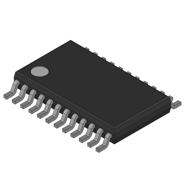
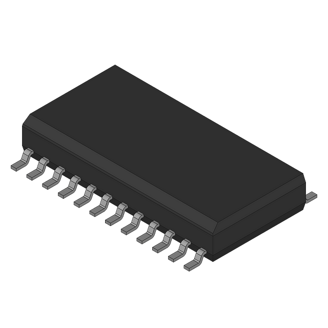
The AD8661 / AD8662 / AD8664 are rail-to-rail output, single-supplyamplifiers that use the Analog Devices, Inc., patentedDigiTrim® trimming technique to achieve low offset voltage.The AD8661 / AD8662 / AD8664 series features extendedoperating ranges, with supply voltages up to 16 V. It alsofeatures low input bias current, wide signal bandwidth,and low input voltage and current noise.The combination of low offset, very low input bias current,and a wide supply range makes these amplifiers useful in a widevariety of applications usually associated with higher priced JFETamplifiers. Systems using high impedance sensors, such asphotodiodes, benefit from the combination of low input biascurrent, low noise, low offset, and wide bandwidth. The wideoperating voltage range meets the demands of high performanceanalog-to-digital converters (ADCs) and digital-to-analogconverters (DACs). Audio applications and medical monitoringequipment can take advantage of the high input impedance, lowvoltage, low current noise, and wide bandwidth.The single AD8661 is available in a narrow 8-lead SOIC packageand a very thin, dual lead, 8-lead LFCSP. The AD8661 SOICpackage is specified over the extended industrial temperaturerange of −40°C to +125°C. The AD8661 LFCSP is specified overthe industrial temperature range of −40°C to +85°C. The AD8662is available in a narrow 8-lead SOIC package and an 8-lead MSOP,both specified over the extended industrial temperature range of−40°C to +125°C. The AD8664 is available in a narrow 14-leadSOIC package and a 14-lead TSSOP, both with an extendedindustrial temperature range of −40°C to +125°C.Applications Sensors Medical equipment Consumer audio Photodiode amplification ADC drivers

AD8676ARMZ-REEL

Part Number : AD8676ARMZ-REEL

Analog Devices Inc.
The AD8676 precision operational amplifier offers ultralow offset, drift, and voltage noise combined with very low input bias currents over the full operating temperature range. The AD8676 is a precision, wide bandwidth op amp featuring rail- to-rail output swings and very low noise. Operation is fully specified from ±5 V to ±15 V.The AD8676 features a rail-to-rail output like that of the OP184, but with wide bandwidth and even lower voltage noise, com-bined with the precision and low power consumption like that of the industry-standard OP07 amplifier. Unlike other low noise, rail-to-rail op amps, the AD8676 has very low input bias current and low input current noise.With typical offset voltage of only 12 μV, offset drift of 0.2 μV/°C, and noise of only 0.10 μV p-p (0.1 Hz to 10 Hz), the AD8676 is perfectly suited for applications where large error sources cannot be tolerated. Precision instrumentation, PLL and other precision filter circuits, position and pressure sensors, medical instrumentation, and strain gage amplifiers benefit greatly from the very low noise, low input bias current, and wide bandwidth. Many systems can take advantage of the low noise, dc precision, and rail-to-rail output swing provided by the AD8676 to maxi-mize SNR and dynamic range.The smaller packages and low power consumption afforded by the AD8676 allow maximum channel density or minimum board size for space-critical equipment.The AD8676 is specified for the extended industrial temperature range (−40°C to +125°C). The AD8676 is available in the 8-lead MSOP, and the popular 8-lead, narrow SOIC; both of which are lead-free packages. MSOP packaged devices are only available in tape and reel format.For the single version of this ultraprecision, rail-to-rail op amp, see the AD8675 data sheet.The AD8675 and AD8676 are members of a growing series of low noise op amps offered by Analog Devices, Inc.ApplicationsPrecision instrumentationPLL filtersLaser diode control loopsStrain gage amplifiersMedical instrumentationThermocouple amplifiers

AD8676ARZ

Part Number : AD8676ARZ

Analog Devices Inc.
The AD8676 precision operational amplifier offers ultralow offset, drift, and voltage noise combined with very low input bias currents over the full operating temperature range. The AD8676 is a precision, wide bandwidth op amp featuring rail- to-rail output swings and very low noise. Operation is fully specified from ±5 V to ±15 V.The AD8676 features a rail-to-rail output like that of the OP184, but with wide bandwidth and even lower voltage noise, com-bined with the precision and low power consumption like that of the industry-standard OP07 amplifier. Unlike other low noise, rail-to-rail op amps, the AD8676 has very low input bias current and low input current noise.With typical offset voltage of only 12 μV, offset drift of 0.2 μV/°C, and noise of only 0.10 μV p-p (0.1 Hz to 10 Hz), the AD8676 is perfectly suited for applications where large error sources cannot be tolerated. Precision instrumentation, PLL and other precision filter circuits, position and pressure sensors, medical instrumentation, and strain gage amplifiers benefit greatly from the very low noise, low input bias current, and wide bandwidth. Many systems can take advantage of the low noise, dc precision, and rail-to-rail output swing provided by the AD8676 to maxi-mize SNR and dynamic range.The smaller packages and low power consumption afforded by the AD8676 allow maximum channel density or minimum board size for space-critical equipment.The AD8676 is specified for the extended industrial temperature range (−40°C to +125°C). The AD8676 is available in the 8-lead MSOP, and the popular 8-lead, narrow SOIC; both of which are lead-free packages. MSOP packaged devices are only available in tape and reel format.For the single version of this ultraprecision, rail-to-rail op amp, see the AD8675 data sheet.The AD8675 and AD8676 are members of a growing series of low noise op amps offered by Analog Devices, Inc.ApplicationsPrecision instrumentationPLL filtersLaser diode control loopsStrain gage amplifiersMedical instrumentationThermocouple amplifiers

AD8676BRMZ

Part Number : AD8676BRMZ

Analog Devices Inc.
The AD8676 precision operational amplifier offers ultralow offset, drift, and voltage noise combined with very low input bias currents over the full operating temperature range. The AD8676 is a precision, wide bandwidth op amp featuring rail- to-rail output swings and very low noise. Operation is fully specified from ±5 V to ±15 V.The AD8676 features a rail-to-rail output like that of the OP184, but with wide bandwidth and even lower voltage noise, com-bined with the precision and low power consumption like that of the industry-standard OP07 amplifier. Unlike other low noise, rail-to-rail op amps, the AD8676 has very low input bias current and low input current noise.With typical offset voltage of only 12 μV, offset drift of 0.2 μV/°C, and noise of only 0.10 μV p-p (0.1 Hz to 10 Hz), the AD8676 is perfectly suited for applications where large error sources cannot be tolerated. Precision instrumentation, PLL and other precision filter circuits, position and pressure sensors, medical instrumentation, and strain gage amplifiers benefit greatly from the very low noise, low input bias current, and wide bandwidth. Many systems can take advantage of the low noise, dc precision, and rail-to-rail output swing provided by the AD8676 to maxi-mize SNR and dynamic range.The smaller packages and low power consumption afforded by the AD8676 allow maximum channel density or minimum board size for space-critical equipment.The AD8676 is specified for the extended industrial temperature range (−40°C to +125°C). The AD8676 is available in the 8-lead MSOP, and the popular 8-lead, narrow SOIC; both of which are lead-free packages. MSOP packaged devices are only available in tape and reel format.For the single version of this ultraprecision, rail-to-rail op amp, see the AD8675 data sheet.The AD8675 and AD8676 are members of a growing series of low noise op amps offered by Analog Devices, Inc.ApplicationsPrecision instrumentationPLL filtersLaser diode control loopsStrain gage amplifiersMedical instrumentationThermocouple amplifiers

AD8676BRMZ-REEL

Part Number : AD8676BRMZ-REEL

Analog Devices Inc.
The AD8676 precision operational amplifier offers ultralow offset, drift, and voltage noise combined with very low input bias currents over the full operating temperature range. The AD8676 is a precision, wide bandwidth op amp featuring rail- to-rail output swings and very low noise. Operation is fully specified from ±5 V to ±15 V.The AD8676 features a rail-to-rail output like that of the OP184, but with wide bandwidth and even lower voltage noise, com-bined with the precision and low power consumption like that of the industry-standard OP07 amplifier. Unlike other low noise, rail-to-rail op amps, the AD8676 has very low input bias current and low input current noise.With typical offset voltage of only 12 μV, offset drift of 0.2 μV/°C, and noise of only 0.10 μV p-p (0.1 Hz to 10 Hz), the AD8676 is perfectly suited for applications where large error sources cannot be tolerated. Precision instrumentation, PLL and other precision filter circuits, position and pressure sensors, medical instrumentation, and strain gage amplifiers benefit greatly from the very low noise, low input bias current, and wide bandwidth. Many systems can take advantage of the low noise, dc precision, and rail-to-rail output swing provided by the AD8676 to maxi-mize SNR and dynamic range.The smaller packages and low power consumption afforded by the AD8676 allow maximum channel density or minimum board size for space-critical equipment.The AD8676 is specified for the extended industrial temperature range (−40°C to +125°C). The AD8676 is available in the 8-lead MSOP, and the popular 8-lead, narrow SOIC; both of which are lead-free packages. MSOP packaged devices are only available in tape and reel format.For the single version of this ultraprecision, rail-to-rail op amp, see the AD8675 data sheet.The AD8675 and AD8676 are members of a growing series of low noise op amps offered by Analog Devices, Inc.ApplicationsPrecision instrumentationPLL filtersLaser diode control loopsStrain gage amplifiersMedical instrumentationThermocouple amplifiers

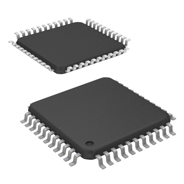
AD9763ASTZ

Part Number : AD9763ASTZ

Analog Devices Inc.
The AD9763/AD9765/AD9767 are dual-port, high speed, 2-channel, 10-/12-/14-bit CMOS DACs. Each part integrates two high quality TxDAC+® cores, a voltage reference, and digital interface circuitry into a small 48-lead LQFP. The AD9763/AD9765/AD9767 offer exceptional ac and dc performance while supporting update rates of up to 125 MSPS.The AD9763/AD9765/AD9767 have been optimized for processing I and Q data in communications applications. The digital interface consists of two double-buffered latches as well as control logic. Separate write inputs allow data to be written to the two DAC ports independent of one another. Separate clocks control the update rate of the DACs.A mode control pin allows the AD9763/AD9765/AD9767 to interface to two separate data ports, or to a single interleaved high speed data port. In interleaving mode, the input data stream is demuxed into its original I and Q data and then latched. The I and Q data is then converted by the two DACs and updated at half the input data rate.The GAINCTRL pin allows two modes for setting the full-scale current (IOUTFS) of the two DACs. IOUTFS for each DAC can be set independently using two external resistors, or IOUTFS for both DACs can be set by using a single external resistor. See the Gain Control Mode section for important date code information on this feature.The DACs utilize a segmented current source architecture combined with a proprietary switching technique to reduce glitch energy and maximize dynamic accuracy. Each DAC provides differential current output, thus supporting single-ended or differential applications. Both DACs of the AD9763, AD9765, or AD9767 can be simultaneously updated and can provide a nominal full-scale current of 20 mA. The full-scale currents between each DAC are matched to within 0.1%.The AD9763/AD9765/AD9767 are manufactured on an advanced, low cost CMOS process. They operate from a single supply of 3.3 V to 5 V and consume 380 mW of power.PRODUCT HIGHLIGHTSThe AD9763/AD9765/AD9767 are members of a pin-compatible family of dual TxDACs providing 8-, 10-, 12-, and 14-bit resolution.Dual 10-/12-/14-Bit, 125 MSPS DACs. A pair of high performance DACs for each part is optimized for low distortion performance and provides flexible transmission of I and Q information.Matching. Gain matching is typically 0.1% of full scale, and offset error is better than 0.02%.Low Power. Complete CMOS dual DAC function operates on 380 mW from a 3.3 V to 5 V single supply. The DAC full-scale current can be reduced for lower power operation, and a sleep mode is provided for low power idle periods.On-Chip Voltage Reference. The AD9763/AD9765/AD9767 each include a 1.20 V temperature-compensated band gap voltage reference.Dual 10-/12-/14-Bit Inputs. The AD9763/AD9765/AD9767 each feature a flexible dual-port interface, allowing dual or interleaved input data.APPLICATIONSCommunicationsBase stationsDigital synthesisQuadrature modulation3D ultrasound

AD9849AKSTZ

Part Number : AD9849AKSTZ

Analog Devices Inc.
The AD9848 and AD9849 are highly integrated CCD signal processors for digital still camera applications. Both include a complete analog front end with A/D conversion, combined with a programmable timing driver. The Precision Timing core allows adjustment of high speed clocks with approximately 1 ns resolution.The AD9848 is specified at pixel rates of 20 MHz, and theAD9849 is specified at 30 MHz. The analog front end includesblack level clamping, CDS, PxGA, VGA, and a 10-bit or 12-bit A/Dconverter. The timing driver provides the high speed CCD clockdrivers for RG and H1–H4. Operation is programmed using a3-wire serial interface.Packaged in a space saving 48-lead LQFP, the AD9848 andAD9849 are specified over an operating temperature range of–20°C to +85°C.APPLICATIONS Digital Still Cameras

ADA4941-1YCPZ-R2

Part Number : ADA4941-1YCPZ-R2

Analog Devices Inc.
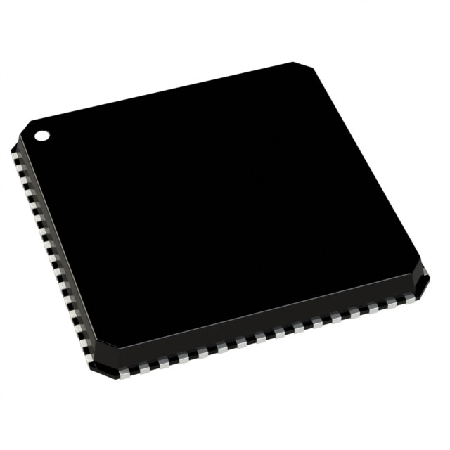
The ADA4941-1 is a low power, low noise differential driver foranalog-to-digital converters (ADCs) up to 18 bits in systemsthat are sensitive to power. The ADA4941-1 is configured in aneasy-to-use, single-ended-to-differential configuration andrequires no external components for a gain of 2 configuration.A resistive feedback network can be added to achieve gains greaterthan 2. The ADA4941-1 provides essential benefits, such as lowdistortion and high SNR that are required for driving highresolution ADCs.With a wide input voltage range (0 V to 3.9 V on a single 5 Vsupply), rail-to-rail output, high input impedance, and a user-adjustablegain, the ADA4941-1 is designed to drive single-supplyADCs with differential inputs found in a variety of low powerapplications, including battery-operated devices and singlesupplydata acquisition systems.The ADA4941-1 is ideal for driving the 16-bit and 18-bitPulSAR® ADCs, such as the AD7687, AD7690, and AD7691.The ADA4941-1 is manufactured on Analog Devices, Inc.,proprietary, second-generation, eXtra fast complementarybipolar (XFCB) process, which enables the amplifier to achieve18-bit performance on low supply currents.The ADA4941-1 is available in a small 8-lead LFCSP as well as astandard 8-lead SOIC and is rated to work over the extendedindustrial temperature range, −40°C to +125°C. Applications Single-supply data acquisition systems Instrumentation Process control Battery-power systems Medical instrumentation

ADF4002BCPZ-RL

Part Number : ADF4002BCPZ-RL

Analog Devices Inc.
The ADF4002 frequency synthesizer is used to implement local oscillators in the up-conversion and down-conversion sections of wireless receivers and transmitters. It consists of a low-noise digital phase frequency detector (PFD), a precision charge pump, a programmable reference divider and programmable N divider. The 14-bit reference counter (R counter), allows selectable REFIN frequencies at the PFD input.A complete phase-locked loop (PLL) can be implemented if the synthesizer is used with an external loop filter and voltage controlled oscillator (VCO). In addition, by programming R and N to 1, the device can be used as a standalone PFD and charge pump.The ADF4002-EP supports defense and aerospace applications (AQEC standard).

ADF4002BCPZ-RL7

Part Number : ADF4002BCPZ-RL7

Analog Devices Inc.
The ADF4002 frequency synthesizer is used to implement local oscillators in the up-conversion and down-conversion sections of wireless receivers and transmitters. It consists of a low-noise digital phase frequency detector (PFD), a precision charge pump, a programmable reference divider and programmable N divider. The 14-bit reference counter (R counter), allows selectable REFIN frequencies at the PFD input.A complete phase-locked loop (PLL) can be implemented if the synthesizer is used with an external loop filter and voltage controlled oscillator (VCO). In addition, by programming R and N to 1, the device can be used as a standalone PFD and charge pump.The ADF4002-EP supports defense and aerospace applications (AQEC standard).

ADF4002BRUZ

Part Number : ADF4002BRUZ

Analog Devices Inc.
The ADF4002 frequency synthesizer is used to implement local oscillators in the up-conversion and down-conversion sections of wireless receivers and transmitters. It consists of a low-noise digital phase frequency detector (PFD), a precision charge pump, a programmable reference divider and programmable N divider. The 14-bit reference counter (R counter), allows selectable REFIN frequencies at the PFD input.A complete phase-locked loop (PLL) can be implemented if the synthesizer is used with an external loop filter and voltage controlled oscillator (VCO). In addition, by programming R and N to 1, the device can be used as a standalone PFD and charge pump.The ADF4002-EP supports defense and aerospace applications (AQEC standard).

ADF4002BRUZ-RL7

Part Number : ADF4002BRUZ-RL7

Analog Devices Inc.
The ADF4002 frequency synthesizer is used to implement local oscillators in the up-conversion and down-conversion sections of wireless receivers and transmitters. It consists of a low-noise digital phase frequency detector (PFD), a precision charge pump, a programmable reference divider and programmable N divider. The 14-bit reference counter (R counter), allows selectable REFIN frequencies at the PFD input.A complete phase-locked loop (PLL) can be implemented if the synthesizer is used with an external loop filter and voltage controlled oscillator (VCO). In addition, by programming R and N to 1, the device can be used as a standalone PFD and charge pump.The ADF4002-EP supports defense and aerospace applications (AQEC standard).

ADM1490EBRMZ

Part Number : ADM1490EBRMZ

Analog Devices Inc.
The ADM1490E / ADM1491E are RS-485/RS-422 transceivers with ±8 kV ESD protection and are suitable for high speed, full-duplex communication on multipoint transmission lines. In particular, the ADM1490E/ADM1491E are designed for use in motor control applications requiring communications at data rates up to 16 Mbps.The ADM1490E / ADM1491E are designed for balanced transmission lines and comply with TIA/EIA-485-A-98. The devices each have a 12 kΩ receiver input impedance for unit load RS-485 operation, allowing up to 32 nodes on the bus.The differential transmitter outputs and receiver inputs feature electrostatic discharge circuitry that provides protection to ±8 kV using the human body model (HBM).The ADM1490E / ADM1491E operate from a single 5 V power supply. Excessive power dissipation caused by bus contention or output shorting is prevented by short-circuit protection and thermal circuitry. Short-circuit protection circuits limit the maximum output current to ±250 mA during fault conditions. A thermal shutdown circuit senses if the die temperature rises above 150°C and forces the driver outputs into a high impedance state under this condition.The receiver of the ADM1490E / ADM1491E contains a fail-safe feature that results in a logic high output state if the inputs are unconnected (floating).The ADM1490E / ADM1491E feature extremely fast and closely matched switching times. Minimal driver propagation delays permit transmission at data rates up to 16 Mbps, and low skew minimizes EMI interference.The ADM1490E/ADM1491E are fully specified over the commercial and industrial temperature ranges. The ADM1490E is available in two packages: a narrow body, 8-lead SOIC and an 8-lead MSOP. The ADM1491E is also available in two packages: a narrow body, 14-lead SOIC and a 10-lead MSOP.APPLICATIONS RS-485/RS-422 interfaces Industrial field networks High data rate motor control Multipoint data transmission systems Single-ended-to-differential signal conversion

ADM3053BRWZ

Part Number : ADM3053BRWZ

Analog Devices Inc.
The ADM3053 is an isolated controller area network (CAN) physical layer transceiver with an integrated isolated dc-to-dc converter. The ADM3053 complies with the ISO 11898 standard.The device employs Analog Devices, Inc., iCoupler® technology to combine a 2-channel isolator, a CAN transceiver, and Analog Devices isoPower® dc-to-dc converter into a single SOIC surface mount package. An on-chip oscillator outputs a pair of square waveforms that drive an internal transformer to provide isolated power. The device is powered by a single 5 V supply realizing a fully isolated CAN solution.The ADM3053 creates a fully isolated interface between the CAN protocol controller and the physical layer bus. It is capable of running at data rates of up to 1 Mbps.The device has current limiting and thermal shutdown features to protect against output short circuits. The part is fully specified over the industrial temperature range and is available in a 20-lead, wide-body SOIC package.The ADM3053 contains isoPower technology that uses high frequency switching elements to transfer power through the transformer. Special care must be taken during printed circuit board (PCB) layout to meet emissions standards. Refer to the AN-0971 Application Note, Control of Radiated Emissions with isoPower Devices, for details on board layout considerations.Applications CAN data buses Industrial field networks

ADN4662BRZ

Part Number : ADN4662BRZ

Analog Devices Inc.
The ADN4662 is a single, CMOS, low voltage differential signaling (LVDS) line receiver offering data rates of over 400 Mbps (200 MHz), and ultralow power consumption. It features a flow-through pinout for easy PCB layout and separation of input and output signals.The device accepts low voltage (310 mV typical) differential input signals and converts them to a single-ended 3 V TTL/ CMOS logic level.The ADN4662 and its companion driver, the ADN4661, offer a new solution to high speed, point-to-point data transmission, and a low power alternative to emitter-coupled logic (ECL) or positive emitter-coupled logic (PECL).ApplicationsPoint-to-point data transmissionMultidrop busesClock distribution networksBackplane receivers

ADN4664BRZ

Part Number : ADN4664BRZ

Analog Devices Inc.
The ADN4664 is a dual, CMOS, low voltage differential signaling (LVDS) line receiver offering data rates of over 400 Mbps (200 MHz) and ultralow power consumption. It features a flow-through pinout for easy PCB layout and separation of input and output signals.The device accepts low voltage (310 mV typical) differential input signals and converts them to a single-ended 3 V TTL/CMOS logic level.The ADN4664 and its companion driver, the ADN4663, offer a new solution to high speed, point-to-point data transmission, and a low power alternative to emitter-coupled logic (ECL) or positive emitter-coupled logic (PECL).ApplicationsPoint-to-point data transmissionMultidrop busesClock distribution networksBackplane receivers

ADP124ACPZ-3.0-R7

Part Number : ADP124ACPZ-3.0-R7

Analog Devices Inc.
The ADP124 / ADP125 are low quiescent current, low dropout linear regulators. They are designed to operate from an input voltage between 2.3 V and 5.5 V and to provide up to 500 mA of output current. The low 130 mV dropout voltage at a 500 mA load improves efficiency and allows operation over a wide input voltage range.The low 210 μA of quiescent current with a 500 mA load makes the ADP124 / ADP125 ideal for battery-operated portable equipment.The ADP124 is capable of 31 fixed-output voltages from 1.75 V to 3.3 V. The ADP125 is the adjustable version of the device and allows the output voltage to be set between 0.8 V and 5.0 V by an external voltage divider.The ADP124/ADP125 are specifically designed for stable operation with tiny 1 μF ceramic input and output capacitors to meet the requirements of high performance, space constrained applications.The ADP124 / ADP125 have an internal soft start that gives a constant start-up time of 350 μs. Short-circuit protection and thermal overload protection circuits prevent damage in adverse conditions. The ADP124 / ADP125 are available in an 8-lead exposed paddle MSOP package. When compared with the standard MSOP package, the exposed paddle MSOP package has lower thermal resistance (θJA). The lower thermal resistance package allows the ADP124 / ADP125 to meet the needs of a variety of portable applications while minimizing the rise in junction temperature.APPLICATIONS Digital camera and audio devices Portable and battery-powered equipment Automatic meter reading (AMR) meters GPS and location management units Medical instrumentation Point of load power

ADP2120ACPZ-1.5-R7

Part Number : ADP2120ACPZ-1.5-R7

Analog Devices Inc.
The ADP2119 / ADP2120 are low quiescent current, synchronous, step-down DC-to -DC regulators in a compact 3mm x3mm LFCSP_WD package. Both Devices use current mode, constant frequency pulse-width modulation (PWM) control scheme for excellent stability and transient response. Under light load condition, they can be configured to operate in pulse frequency modulation (PFM) mode that reduces switching frequency to save power.The ADP2119/ADP2120 can support input voltages from 2.3V to 5.5V. The output voltage can be adjusted from 0.6V to input voltage (VIN) for the adjustable version, while the fixed output version is available in preset output voltage options of 3.3V, 2.5V, 1.8V, 1.5V ,1.2V and 1.0V. The ADP2119/ADP2120 require minimal external parts and provide a high efficiency solution with their integrated power switches, synchronous rectifier, and internal compensation. Each IC draws less than 3 μA current from the input source when it is disabled. Other key features include under voltage lockout(UVLO), integrated soft start to limit inrush current at startup, overvoltage protection (OVP), over current protection (OCP) and thermal shutdown (TSD).APPLICATIONS Point of load conversion Communications and networking equipment Industrial and instrumentation Consumer electronics Medical appliances

ADP2323ACPZ-R7

Part Number : ADP2323ACPZ-R7

Analog Devices Inc.
The ADP2323 is a full featured, dual output, step-down dc-to-dc regulator based on current-mode architecture. The ADP2323 integrates two high-side power MOSFETs and two low-side drivers for the external N-channel MOSFETs. The two pulse-width mod-ulation (PWM) channels can be configured to deliver dual 3 A outputs or a parallel-to-single 6 A output. The regulator operates from input voltages of 4.5 V to 20 V, and the output voltage can be as low as 0.6 V.The switching frequency can be programmed between 250 kHz and 1.2 MHz, or synchronized to an external clock to minimize interference in multirail applications. The dual PWM channels run 180° out of phase, thereby reducing input current ripple as well as reducing the size of the input capacitor.The bidirectional synchronization pin can be programmed at a 60°, 90°, or 120° phase shift, providing the possibility for a stackable multiphase power solution.The ADP2323 can be set to operate in pulse-frequency modulation (PFM) mode at a light load for higher efficiency or in forced PWM for noise sensitive applications. External compensation and soft start provide design flexibility. Independent enable inputs and power good outputs provide reliable power sequencing. To enhance system reliability, the device also includes undervoltage lockout (UVLO), overvoltage protection (OVP), overcurrent pro-tection (OCP), and thermal shutdown (TSD).The ADP2323 operates over the −40°C to +125°C junction temperature range and is available in a 32-lead LFCSP_WQ package.APPLICATION Communication infrastructure Networking and servers Industrial and instrumentation Healthcare and medical Intermediate power rail conversion DC-to-dc point of load applications

ADR3420ARJZ-R2

Part Number : ADR3420ARJZ-R2

Analog Devices Inc.
The ADR3412 / ADR3420 / ADR3425 / ADR3430 / ADR3433 / ADR3440 / ADR3450 are low-cost, low-power, high precision voltage references, featuring ± 0.1% initial accuracy, low operating current and low output noise in a small SOT23 package. For high accuracy, output voltage and temperature coefficient are trimmed digitally during final assembly using Analog Devices’ proprietary DigiTrim® technology. Stability and reliability are further improved by the devices’ low output voltage hysteresis and low long-term output voltage drift. Furthermore, the low operating current of the device (100 μA max) facilitates usage in low-power devices, while its low output noise helps maintain signal integrity in critical signal processing systems.These CMOS are available in a wide range of output voltages, all of which are specified over the industrial temperature range of −40°C to +125 °C.APPLICATIONS Precision data acquisition systems Industrial instrumentation Medical devices Battery-powered devices

Displaying 421 - 440 of 93400

Latest Parts

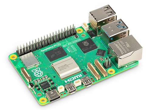
SC1112

Raspberry Pi

$79.61 - $86.40

IN STOCK 10275
Buy

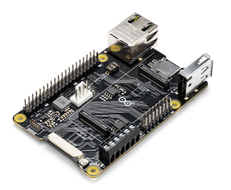
ASX00049

Arduino

* $39.41 - * $44.41

IN STOCK 3132
Buy

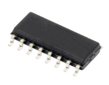
AD96685BRZ

Analog Devices Inc.

$1.72 - * $11.79

IN STOCK 4921
Buy

Reference Designs

RD006

Wurth Elektronik

RD006 - 3 W Dual-output isolated auxiliary supply for communication interfaces and measurement systems

CN0583

Analog Devices Inc.

Multistandard Micropower Verified Smoke Detection System-on-Module

Technical Resources

EVALUATION KITS

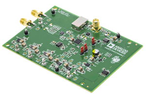
EVAL-AD7124-8SDZ

Analog Devices Inc.

$71.02 - * $75.98

IN STOCK 808
Buy
View All