AD847SQ
Part Number : AD847SQ
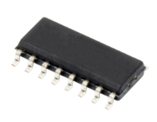
Analog Devices Inc.The AD847 represents a breakthrough in high speed amplifiers offing superior ac & dc perfomance and low power, all at low cost. The excellent dc performance is demonstrated by its ±5 V specifications which include an open-loop gain of 3500 V/V (500 Ohm load) and low input offset voltage of 0.5 mV. Common-mode rejection is a minimum of 78 dB. Output voltage swing is ±3 V into loads as low as 150 Ohm. Analog Devices also offers over 30 other high speed amplifiers from the low noise AD829 (1.7nV/(root)Hz) to the ultimate video amplifier, the AD811, which features 0.01% differential gain and 0.01° differential phase.
AD8610ARMZ-R7
Part Number : AD8610ARMZ-R7
Analog Devices Inc.The AD8610 (single) and AD8620 (dual) are very high precision JFET input amplifiers featuring ultralow offset voltage and drift, very low input voltage and current noise, very low input bias current, and wide bandwidth. Unlike many JFET amplifiers, the AD8610 input bias current is low over the entire operating temperature range. The AD8610 is stable with capacitive loads of over 1000 pF in noninverting unity gain; much larger capacitive loads can be driven easily at higher noise gains. The AD8610 swings to within 1.2 V of the supplies even with a 1 k Ω load, maximizing dynamic range even with limited supply voltages. Outputs slew at 50 V/µs in either inverting or noninverting gain configurations, and settle to 0.01% accuracy in less than 600 ns. Combined with the high input impedance, great precision, and very high output drive, the AD8610 is an ideal amplifier for driving high performance A/D inputs and buffering D/A converter outputs. Applications for the AD8610 and AD8620 include electronic instruments; ATE amplification, buffering, and integrator circuits; CAT/MRI/Ultrasound medical instrumentation; instrumentation quality photodiode amplification; fast precision filters (including PLL filters); and high quality audio. The AD8610 is fully specified over the extended industrial (-40ºC.to +125ºC.temperature range. The AD8610 is available in the narrow 8-lead SOIC and the tiny MSOP8 surface-mount packages. The AD8620 is available in the narrow 8-lead SOIC package. MSOP8 packaged devices are available only in tape and reel.
AD8630ARUZ
Part Number : AD8630ARUZ
Analog Devices Inc.This amplifier has ultralow offset, drift, and bias current. The AD8628/AD8629/AD8630 are wide bandwidth auto-zero amplifiers featuring rail-to-rail input and output swing and low noise. Operation is fully specified from 2.7 V to 5 V single supply (±1.35 V to ±2.5 V dual supply).The AD8628/AD8629/AD8630 provide benefits previously found only in expensive auto-zeroing or chopper-stabilized amplifiers. Using Analog Devices, Inc., topology, these zero-drift amplifiers combine low cost with high accuracy and low noise. No external capacitor is required. In addition, the AD8628/ AD8629/AD8630 greatly reduce the digital switching noise found in most chopper-stabilized amplifiers.With an offset voltage of only 1 μV, drift of less than 0.005 μV/°C, and noise of only 0.5 μV p-p (0.1 Hz to 10 Hz), the AD8628/AD8629/AD8630 are suited for applications where error sources cannot be tolerated. Position and pressure sensors, medical equipment, and strain gage amplifiers benefit greatly from nearly zero drift over their operating temperature range. Many systems can take advantage of the rail-to-rail input and output swings provided by the AD8628/AD8629/AD8630 to reduce input biasing complexity and maximize SNR.The AD8628/AD8629/AD8630 are specified for the extended industrial temperature range (−40°C to +125°C). The AD8628 is available in tiny 5-lead TSOT, 5-lead SOT-23, and 8-lead narrow SOIC plastic packages. The AD8629 is available in the standard 8-lead narrow SOIC and MSOP plastic packages. The AD8630 quad amplifier is available in 14-lead narrow SOIC and 14-lead TSSOP plastic packages. See the Ordering Guide section in the data sheet for automotive grades.APPLICATIONS Automotive sensors Pressure and position sensors Strain gage amplifiers Medical instrumentation Thermocouple amplifiers Precision current sensing Photodiode amplifiers
AD8642ARMZ
Part Number : AD8642ARMZ
Analog Devices Inc.The AD8641/AD8642/AD8643 are low power, precision JFET input amplifiers featuring extremely low input bias current and rail-to-rail output. The ability to swing nearly rail-to-rail at the input and rail-to-rail at the output enables designers to buffer CMOS DACs, ASICs, and other wide output swing devices in single-supply systems. The outputs remain stable with capacitive loads of more than 500 pF.The AD8641/AD8642/AD8643 are suitable for applications utilizing multichannel boards that require low power to manage heat. Other applications include photodiodes, ATE reference level drivers, battery management, and industrial controls.The AD8641/AD8642/AD8643 are fully specified over the extended industrial temperature range of –40°C to +125°C. The AD8641 is available in 5-lead SC70 and 8-lead SOIC lead-free packages. The AD8642 is available in 8-lead MSOP and 8-lead SOIC lead-free packages. The AD8643 is available in 14-lead SOIC and 16-lead, 3 mm × 3 mm, LFCSP lead-free packages.Applications Line-/battery-powered instruments Photodiode amplifiers Precision current sensing Medical instrumentation Industrial controls Precision filters Portable audio ATE
AD8642ARZ
Part Number : AD8642ARZ
Analog Devices Inc.The AD8641/AD8642/AD8643 are low power, precision JFET input amplifiers featuring extremely low input bias current and rail-to-rail output. The ability to swing nearly rail-to-rail at the input and rail-to-rail at the output enables designers to buffer CMOS DACs, ASICs, and other wide output swing devices in single-supply systems. The outputs remain stable with capacitive loads of more than 500 pF.The AD8641/AD8642/AD8643 are suitable for applications utilizing multichannel boards that require low power to manage heat. Other applications include photodiodes, ATE reference level drivers, battery management, and industrial controls.The AD8641/AD8642/AD8643 are fully specified over the extended industrial temperature range of –40°C to +125°C. The AD8641 is available in 5-lead SC70 and 8-lead SOIC lead-free packages. The AD8642 is available in 8-lead MSOP and 8-lead SOIC lead-free packages. The AD8643 is available in 14-lead SOIC and 16-lead, 3 mm × 3 mm, LFCSP lead-free packages.Applications Line-/battery-powered instruments Photodiode amplifiers Precision current sensing Medical instrumentation Industrial controls Precision filters Portable audio ATE
AD977AARSZ
Part Number : AD977AARSZ
Analog Devices Inc.The AD977 / AD977A is a high speed, low power 16-bit A/D converter that operates from a single 5 V supply. The AD977A has a throughput rate of 200 kSPS whereas the AD977 has a throughput rate of 100 kSPS. Each part contains a successive approximation, switched capacitor ADC, an internal 2.5 V reference, and a high speed serial interface. The ADC is factory calibrated to minimize all linearity errors. The AD977 / AD977A is specified for full scale bipolar input ranges of ±10 V, ±5 V and ±3.3 V, and unipolar ranges of 0 V to 10 V, 0 V to 5 V and 0 V to 4 V.The AD977 / AD977A is comprehensively tested for ac parameters such as SNR and THD, as well as the more traditional dc parameters of offset, gain and linearity.PRODUCT HIGHLIGHTS Fast Throughput The AD977 / AD977A is a high speed, 16-bit ADC based on a factory calibrated switched capacitor architecture. Single-Supply Operation The AD977 / AD977A operates from a single 5 V supply and dissipates only 100 mW max. Comprehensive DC and AC Specifications In addition to the traditional specifications of offset, gain and linearity, the AD977 / AD977A is fully tested for SNR and THD.
AD9850BRSZ-REEL
Part Number : AD9850BRSZ-REEL
Analog Devices Inc.The AD9850 is a highly integrated device that uses advanced DDS technology coupled with an internal high speed, high performance, D/A converter and comparator, to form a complete digitally programmable frequency synthesizer and clock generator function. When referenced to an accurate clock source, the AD9850 generates a spectrally pure, frequency/ phase-programmable, analog output sine wave. This sine wave can be used directly as a frequency source or converted to a square wave for agile-clock generator applications. The AD9850’s innovative high speed DDS core provides a 32-bit frequency tuning word, which results in an output tuning resolution of 0.0291 Hz, for a 125 MHz reference clock input. The AD9850’s circuit architecture allows the generation of output frequencies of up to one-half the reference clock frequency (or 62.5 MHz), and the output frequency can be digitally changed (asynchronously) at a rate of up to 23 million new frequencies per second. The device also provides five bits of digitally controlled phase modulation, which enables phase shifting of its output in increments of 180°, 90°, 45°, 22.5°, 11.25° and any combination thereof. The AD9850 also contains a high speed comparator that can be configured to accept the (externally) filtered output of the DAC to generate a low jitter square wave output. This facilitates the device’s use as an agile clock generator function.The frequency tuning, control, and phase modulation words are loaded into the AD9850 via a parallel byte or serial loading format. The parallel load format consists of five iterative loads of an 8-bit control word (byte). The first byte controls phase modulation, power-down enable, and loading format; bytes 2–5 comprise the 32-bit frequency tuning word. Serial loading is accomplished via a 40-bit serial data stream on a single pin. The AD9850 Complete-DDS uses advanced CMOS technology to provide this breakthrough level of functionality and performance on just 155 mW of power dissipation (+3.3 V supply).The AD9850 is available in a space saving 28-lead SSOP, surface mount package. It is specified to operate over the extended industrial temperature range of –40°C to +85°C
ADG333ABRZ
Part Number : ADG333ABRZ
Analog Devices Inc.The ADG333A is a monolithic complementary metal-oxidesemiconductor (CMOS) device comprising four independentlyselectable single-pole, double-throw (SPDT) switches. It isdesigned on a linear compatible CMOS (LC2MOS) process,which provides low power dissipation yet achieves a highswitching speed and a low on resistance.The on-resistance profile is very flat over the full analog inputrange, ensuring good linearity and low distortion when switchingaudio signals. High switching speed also makes the device suitablefor video signal switching. CMOS construction ensures ultralowpower dissipation, making the device ideally suited for portable,battery-powered instruments.When they are on, each switch conducts equally well in bothdirections and has an input signal range that extends to thepower supplies. In the off condition, signal levels up to thesupplies are blocked. All switches exhibit break-before-makeswitching action for use in multiplexer applications. Low chargeinject is inherent in the design.Product Highlights Extended signal range. The ADG333A is fabricated on an enhanced LC2MOS process, giving an increased signal range which extends to the supply rails. Low power dissipation. Low RON. Single-supply operation. For applications in which the analog signal is unipolar, the ADG333A can be operated from a single rail power supply. The device is fully specified with a single 12 V supply. Applications Audio and video switching Battery-powered systems Test equipment Communication systems
ADG411BRUZ
Part Number : ADG411BRUZ
Analog Devices Inc.The ADG411 is a monolithic CMOS device comprising four independently selectable switches. It is designed on an enhanced LC2MOS process which provides low power dissipation yet gives high switching speed and low on resistance.The ADG411 switches are turned on with a logic low on the appropriate control input. Each switch conducts equally well in both directions when ON and each has an input signal range that extends to the supplies. All switches exhibit break-before-make switching action for use in multiplexer applications. Inherent in the design is low charge injection for minimum transients when switching the digital inputs.
ADG412BRUZ
Part Number : ADG412BRUZ
Analog Devices Inc.The ADG411, ADG412, and ADG413 are monolithic CMOS devices comprising four independently selectable switches. They are designed on an enhanced LC2MOS process which provides low power dissipation yet gives high switching speed and low on resistance.The on resistance profile is very flat over the full analog input range ensuring excellent linearity and low distortion when switching audio signals. Fast switching speed coupled with high signal bandwidth also make the parts suitable for video signal switching. CMOS construction ensures ultralow power dissipation, making the parts ideally suited for portable and battery-powered instruments.The ADG411, ADG412, and ADG413 contain four independent SPST switches. The ADG411 and ADG412 differ only in that the digital control logic is inverted. The ADG411 switches are turned on with a logic low on the appropriate control input, while a logic high is required for the ADG412. The ADG413 has two switches with digital control logic similar to that of the ADG411 while the logic is inverted on the other two switches.Each switch conducts equally well in both directions when on, and each has an input signal range that extends to the supplies. In the off condition, signal levels up to the supplies are blocked. All switches exhibit break-before-make switching action for use in multiplexer applications. Inherent in the design is low charge injection for minimum transients when switching the digital inputs.PRODUCT HIGHLIGHTS Extended signal range The ADG411, ADG412, and ADG413 are fabricated on an enhanced LC2MOS, giving an increased signal range which extends fully to the supply rails. Ultralow power dissipation. Low RON Break-before-make switching This prevents channel shorting when the switches are configured as a multiplexer. Single-supply operation For applications where the analog signal is unipolar, the ADG411, ADG412, and ADG413 can be operated from a single-rail power supply. The parts are fully specified with a single 12 V power supply and remain functional with single supplies as low as 5 V.APPLICATIONS Audio and video switching Automatic test equipment Precision data acquisition Battery-powered systems Sample-and-hold systems Communication systems
ADM211EARUZ
Part Number : ADM211EARUZ
Analog Devices Inc.The ADM2xxE is a family of robust RS-232 and V.28 interface devices which operates from a single +5 V power supply. These products are suitable for operation in harsh electrical environments and are compliant with the EU directive on EMC (89/336/ EEC). Both the level of emissions and immunity are in compliance. EM immunity includes ESD protection in excess of ±15 kV on all I-O lines (1000-4-2), Fast Transient Burst protection (1000-4-4) and Radiated Immunity (1000-4-3). EM emissions include radiated and conducted emissions as required by Information Technology Equipment EN55022, CISPR22.All devices fully conform to the EIA-232E and CCITT V.28 specifications and operate at data rates up to 230 kbps. Shutdown and Enable control pins are provided on some of the products. The shutdown function on the ADM211E disables the charge pump and all transmitters and receivers. On the ADM213E the charge pump, all transmitters, and three of the five receivers are disabled. The remaining two receivers remain active thereby allowing monitoring of peripheral devices. This feature allows the device to be shut down until a peripheral device begins communication. The active receivers can alert the processor which can then take the ADM213E out of the shutdown mode. Operating from a single +5 V supply, four external 0.1 µF capacitors are required. The ADM206E is available in a 24-pin SO package. The ADM207E and ADM208E are available in 24-pin DIP, SO, SSOP and TSSOP packages. The ADM211E and ADM213E are available in 28-pin SO, SSOP and TSSOP packages. All products are backward compatible with earlier ADM2xx products facilitating easy upgrading of older designs.
ADM242ARZ
Part Number : ADM242ARZ
Analog Devices Inc.The ADM222, ADM232A, ADM242 are a family of high-speedRS-232 line drivers/receivers offering transmission rates up to200 kB/s. Operating from a single 5 V power supply, a highlyefficient on-chip charge pump using small (0.1 µF) externalcapacitors allows RS-232 bipolar levels to be developed. TwoRS-232 drivers and two RS-232 receivers are provided oneach device.The devices are fabricated on BiCMOS, an advanced mixedtechnology process that combines low power CMOS with highspeedbipolar circuitry. This allows for transmission rates up to200 kB/s, yet minimizes the quiescent power supply current tounder 5 mA.The ADM232A is a pin-compatible, high-speed upgrade for theAD232 and for the ADM232L. It is available in 16-lead DIPand in both narrow and wide surface-mount (SOIC) packages.The ADM222 contains an additional shutdown (SHDN) functionthat may be used to disable the device, thereby reducing thesupply current to 0.1 µA. During shutdown, all transmit/receivefunctions are disabled. The ADM222 is available in 18-leadDIP and in a wide surface-mount (SOIC) package.The ADM242 combines both shutdown (SHDN) and enable(EN) functions. The shutdown function reduces the supplycurrent to 0.1 mA. During shutdown, the transmitters are disabledbut the receivers continue to operate normally. Theenable function allows the receiver outputs to be disabledthereby facilitating sharing a common bus. The ADM242 isavailable in 18-lead DIP and in a wide surface-mount (SOIC)package.Applications Computers Peripherals Modems Printers Instruments
ADP3338AKCZ-2.85R7
Part Number : ADP3338AKCZ-2.85R7
Analog Devices Inc.The ADP3338 is a member of the ADP330x family ofprecision low dropout anyCAP® voltage regulators. The ADP3338 operates with an input voltage range of +2.7 V to +8 V and delivers a load current up to 1 A. The ADP3338 stands out from the conventional LDOs with a novel architecture and an enhanced process that enables it to offer performance advantages and higher output currentthan its competition. Its patented design requires only a 1.0 µF output capacitor for stability. This device is insensitive to output capacitor Equivalent Series Resistance (ESR), and is stable with any good quality capacitor, including ceramic (MLCC) types for space-restricted applications.The ADP3338 achieves exceptional accuracy of ±0.9% at room temperature and ±1.8% over temperature, line and load variations. The dropout voltage of the ADP3338 is only 200 mV (typical) at 1 A. This device also includes a safety current limit and thermal overload protection. The ADP3338 has ultralow quiescent current 130 µA (typ) in light load situations.APPLICATIONS Notebook, palmtop computers SCSI terminators Battery-powered systems Bar code scanners Camcorders, cameras Home entertainment systems Networking systems DSP/ASIC supplies
ADSP-21160NCBZ-100
Part Number : ADSP-21160NCBZ-100
Analog Devices Inc.The ADSP-21160N SHARC® DSP is the second iteration of the ADSP-21160. Built in a 0.18 micron CMOS process, it offers higher performance and lower power consumption than its predecessor, the ADSP-21160M. Easing portability, the ADSP-21160N is application source code compatible with first generation ADSP-2106x SHARC DSPs in SISD (Single Instruction, Single Data) mode. To take advantage of the processor’s SIMD (Single Instruction, Multiple Data) capability, some code changes are needed. Like other SHARCs, the ADSP-21160N is a 32-bit processor that is optimized for high performance DSP applications. The ADSP-21160N includes a 100 MHz core, a dual-ported on-chip SRAM, an integrated I/O processor with multiprocessing support, and multiple internal buses to eliminate I/O bottlenecks.The ADSP-21160N introduces Single-Instruction, Multiple-Data (SIMD) processing. Using two computational units (ADSP-2106x SHARC DSPs have one), the ADSP-21160N can double performance versus the ADSP-2106x on a range of DSP algorithms.The ADSP-21160N continues SHARC’s industry-leading standards of integration for DSPs, combining a high-performance 32-bit DSP core with integrated, on-chip system features. These features include a 4M-bit dual ported SRAM memory, host processor interface, I/O processor that supports 14 DMA channels, two serial ports, six link ports, external parallel bus, and glueless multiprocessing.
ADSP-21161NKCAZ100
Part Number : ADSP-21161NKCAZ100
Analog Devices Inc.The ADSP-21161 SHARC® DSP is the newest member of the Super Harvard Architecture (SHARC) family of programmable DSPs. Capable of 600 million math operations per second (MFLOPs), the ADSP-21161 sets a new level of performance for low-cost SHARC DSPs - more than three times the performance for comparable models at about the same price. Its road map includes a cost-effective path to 1200 MFLOPS for $5 per unit and a performance-driven path to 10 GFLOPS and beyond.'This newest edition to the SHARC family will open more possibilities for designers to design-in high performance digital signal processing into client-side applications and should help others reconsider applications they couldn’t do before with a single chip,' said Will Strauss, president of Forward Concepts. 'Analog Devices will certainly maintain customer loyalty with this road map.' The ADSP-21161 DSP is the second member of the SHARC DSP family of 32-bit floating-point programmable DSPs to be based on a SIMD core architecture that is optimized for digital signal processing performance. Like all SHARCs, the ADSP-21161 is code-compatible with all other members of the family and supports both fixed- and floating-point data types. The ADSP-21161 lowers the price for SIMD SHARC DSP performance and is an outstanding DSP solution for many price-sensitive applications.State-of-the-Art Development Tools The ADSP-21161, like all SHARC processors, is supported by a complete set of software and hardware development tools. The VisualDSP++® tool set offered by Analog Devices includes an optimizing C/C++ compiler, integrated development environment (IDE), assembler, linker, splitter and cycle accurate simulator that support both C and assembly debugging. Emulation support is JTAG-based and ADI offers USB, PCI, and Ethernet based emulators. SHARC DSP Roadmap There are two code-compatible paths that the SHARC DSP roadmap will follow. One optimized for high-performance multiprocessing systems and the other for price/performance. Performance is the key for multiprocessing applications and this is the reason that ADI will offer 10 GFLOP SHARC DSPs in the future. On-chip memory sizes will be balanced to match this performance with memories increasing to unprecedented levels (64 Mbit) using newly developed technologies.Industry leading price/performance will be the driver on the other path of the roadmap. In the future, these SHARC DSPs will offer an increase in performance to 1200 MFLOPs while decreasing price to as low as $5.00. This is required to support new technologies that demand substantial signal processing performance at consumer price points.
ADUC834BSZ
Part Number : ADUC834BSZ
Analog Devices Inc.The ADuC834 is a complete smart transducer front end,integrating two high resolution - ADCs, an 8-bit MCU, andprogram/data Flash/EE memory on a single chip.The two independent ADCs (primary and auxiliary) include atemperature sensor and a PGA (allowing direct measurement oflow level signals). The ADCs with on-chip digital filtering andprogrammable output data rates are intended for the measurementof wide dynamic range, low frequency signals, such as those inweigh scale, strain-gage, pressure transducer, or temperaturemeasurement applications.The device operates from a 32 kHz crystal with an on-chip PLLgenerating a high frequency clock of 12.58 MHz. This clock isrouted through a programmable clock divider from which the MCUcore clock operating frequency is generated. The microcontrollercore is an 8052 and therefore 8051 instruction set compatiblewith 12 core clock periods per machine cycle.62 Kbytes of nonvolatile Flash/EE program memory, 4 Kbytes ofnonvolatile Flash/EE data memory, and 2304 bytes of data RAMare provided on-chip. The program memory can be configuredas data memory to give up to 60 Kbytes of NV data memory indata logging applications.On-chip factory firmware supports in-circuit serial download anddebug modes (via UART), as well as single-pin emulation modevia the EA pin. The ADuC834 is supported by a QuickStart™development system featuring low cost software and hardwaredevelopment tools.Applications Intelligent sensors Weigh scales Portable instrumentation, battery-powered systems 4–20 mA transmitters Data logging Precision system monitoring
ADUC836BSZ
Part Number : ADUC836BSZ
Analog Devices Inc.The ADuC836 is a complete smart transducer front end, integratingtwo high resolution Σ-Δ ADCs, an 8-bit MCU, and program/dataFlash/EE memory on a single chip.The two independent ADCs (primary and auxiliary) include atemperature sensor and a PGA (allowing direct measurementof low level signals). The ADCs with on-chip digital filtering andprogrammable output data rates are intended for the measurementof wide dynamic range, low frequency signals, such as thosein weigh scale, strain gage, pressure transducer, or temperaturemeasurement applications.The device operates from a 32 kHz crystal with an on-chip PLLgenerating a high frequency clock of 12.58 MHz. This clock isrouted through a programmable clock divider from which the MCUcore clock operating frequency is generated. The microcontrollercore is an 8052 and therefore 8051 instruction set compatiblewith 12 core clock periods per machine cycle.62 Kbytes of nonvolatile Flash/EE program memory, 4 Kbytes ofnonvolatile Flash/EE data memory, and 2304 bytes of data RAMare provided on-chip. The program memory can be configured asdata memory to give up to 60 Kbytes of NV data memory in datalogging applications.On-chip factory firmware supports in-circuit serial download anddebug modes (via UART), as well as single-pin emulation modevia the EA pin. The ADuC836 is supported by a QuickStart™development system featuring low cost software and hardware development tools.Applications Intelligent sensors Weigh scales Portable instrumentation, battery-powered systems 4–20 mA transmitters Data logging Precision system monitoring
CMP402GSZ
Part Number : CMP402GSZ
Analog Devices Inc.The CMP401 and CMP402 are 23 ns and 65 ns quad comparatorswith separate input and output supplies. Separate suppliesenable the input stage to be operated from +3 V to as high as ±6 V.The output can be supplied with either 3 V or 5 V as determinedby the interface logic or available supplies. Independent inputand output supplies combined with fast propagation make theCMP401 and CMP402 excellent choices for interfacing toportable instrumentation.The CMP401 and CMP402 are specified over the extended industrial(–40°C to +125°C) temperature range. Both are available innarrow 16-lead SOIC surface-mount packages and 16-lead TSSOP.Applications Battery-operated instrumentation Line receivers Level translators Read channel detection
DC760A
Part Number : DC760A
Analog Devices Inc.The LT3472 dual channel switching regulator generates positive and negative outputs for biasing CCD imagers. The device delivers up to –8V at 50mA and 15V at 20mA from a lithium-ion cell, providing bias for many popular CCD imagers. Switching at 1.1MHz, the LT3472 uses tiny, low profile capacitors and inductors and generates low noise outputs that are easy to filter. Schottky diodes are internal and the output voltages are set with one resistor per channel, reducing external component count. The entire solution is less than 1mm profile and occupies just 50mm2.Internal sequencing circuitry disables the negative channel until the positive channel has reached 88% of its final value, ensuring that the sum of the two outputs is always positive. Separate soft-start capacitors for each output allow the ramp of each output to be independently controlled.The LT3472 is available in a low profile (0.75mm) 10-pin 3mm × 3mm DFN package.Applications CCD Bias TFT LCD Bias OLED Bias ± Rail Generation for Op Amps
DC782A-E
Part Number : DC782A-E
Analog Devices Inc.The LTC2245 is a 14-bit 10Msps, low power 3V A/D converter designed for digitizing high frequency, wide dynamic range signals. The LTC2245 is perfect for demanding imaging and communications applications with AC performance that includes 74.4dB SNR and 90dB SFDR for signals well beyond the Nyquist frequency.DC specs include ±1LSB INL (typ), ±0.5LSB DNL (typ) and no missing codes over temperature. The transition noise is a low 1LSBRMS.A single 3V supply allows low power operation. A separate output supply allows the outputs to drive 0.5V to 3.6V logic.A single-ended CLK input controls converter operation. An optional clock duty cycle stabilizer allows high performance at full speed for a wide range of clock duty cycles.Applications Wireless and Wired Broadband Communication Imaging Systems Spectral Analysis Portable Instrumentation


