
AD8226BRMZ-RL
Part Number : AD8226BRMZ-RL
Analog Devices Inc.The AD8226 is a low cost, wide supply range instrumentation amplifier that requires only one external resistor to set any gain between 1 and 1000.The AD8226 is designed to work with a variety of signal voltages. A wide input range and rail-to-rail output allow the signal to make full use of the supply rails. Because the input range also includes the ability to go below the negative supply, small signals near ground can be amplified without requiring dual supplies. The AD8226 operates on supplies ranging from ±1.35 V to ±18 V for dual supplies and 2.2 V to 36 V for single supply.The robust AD8226 inputs are designed to connect to real-world sensors. In addition to its wide operating range, the AD8226 can handle voltages beyond the rails. For example, with a ±5 V supply, the part is guaranteed to withstand ±35 V at the input with no damage. Minimum as well as maximum input bias currents are specified to facilitate open wire detection.The AD8226 is perfect for multichannel, space-constrained industrial applications. Unlike other low cost, low power instrumentation amplifiers, the AD8226 is designed with a minimum gain of 1 and can easily handle ±10 V signals. With its MSOP package and 125°C temperature rating, the AD8226 thrives in tightly packed, zero airflow designs.The AD8226 is available in 8-lead MSOP and SOIC packages, and is fully specified for −40°C to +125°C operation.For a device with a similar package and performance as the AD8226 but with gain settable from 5 to 1000, consider using the AD8227.ApplicationsIndustrial process controlsBridge amplifiersMedical instrumentationPortable data acquisitionMultichannel systems

AD8274ARMZ-R7
Part Number : AD8274ARMZ-R7
Analog Devices Inc.The AD8274 is a difference amplifier that delivers excellent ac and dc performance. Built on Analog Devices, Inc., proprietary iPolar® process and laser-trimmed resistors, AD8274 achieves a breakthrough in distortion vs. current consumption and has excellent gain drift, gain accuracy, and CMRR.Distortion in the audio band is an extremely low 0.00025% (112 dB) at a gain of ½ and 0.00035% (109 dB) at a gain of 2 while driving a 600 Ω load.With supply voltages up to ±18 V (+36 V single supply), the AD8274 is well suited for measuring large industrial signals. Additionally, the part’s resistor divider architecture allows it to measure voltages beyond the supplies.With no external components, the AD8274 can be configured as a G = ½ or G = 2 difference amplifier. For single-ended applications that need high gain stability or low distortion performance, the AD8274 can also be configured for several gains ranging from −2 to +3.The excellent distortion and dc performance of the AD8274, along with its high slew rate and bandwidth, make it an excellent ADC driver. Because of the part’s high output drive, it also makes a very good cable driver.The AD8274 only requires 2.6 mA maximum supply current. It is specified over the industrial temperature range of −40°C to +85°C and is fully RoHS compliant. For the dual version, see the AD8273 data sheet.Applications ADC driver High performance audio Instrumentation amplifier building blocks Level translators Automatic test equipment Sine/cosine encoders

AD8275ARMZ-RL
Part Number : AD8275ARMZ-RL
Analog Devices Inc.The AD8275 is a G=0.2 difference amplifier that can be used totranslate +/-10V signals to a +4V level. It solves the problemtypically encountered in industrial and instrumentation where+/-10V signals must be interfaced to a single supply 4V or 5VADC. The AD8275 interfaces the two signal levels, simplifyingdesign.The AD8275 has fast settling time of 450 ns and low distortion,making it suitable for driving medium speed successive approximation(SAR) ADCs. Its wide input voltage range and rail-torailoutputs make it an easy to use building block. Single-supplyoperation reduces the power consumption of the amplifier andhelps to protect the ADC from overdrive conditions. Internal, matched, precision laser-trimmed resistors ensurelow gain error, low gain drift of 1 ppm/°C (maximum), andhigh common-mode rejection of 80 dB. Low offset and lowoffset drift, combined with its fast settling time, make theAD8275 suitable for a variety of data acquisition applicationswhere accurate and quick capture is required. The AD8275 can be used as an analog front end, or it can followbuffers to level translate high voltages to a voltage range acceptedby the ADC. In addition, the AD8275 can be configured fordifferential outputs if used with a differential ADC. The AD8275 is available in a space-saving, 8-lead MSOP and is specified for performance over the −40°C to +85°C temperature range.ApplicationsLevel TranslatorADC DriverInstrumentation Amplifier Building BlockAutomated test equipment
AD8275BRMZ
Part Number : AD8275BRMZ
Analog Devices Inc.The AD8275 is a G=0.2 difference amplifier that can be used totranslate +/-10V signals to a +4V level. It solves the problemtypically encountered in industrial and instrumentation where+/-10V signals must be interfaced to a single supply 4V or 5VADC. The AD8275 interfaces the two signal levels, simplifyingdesign.The AD8275 has fast settling time of 450 ns and low distortion,making it suitable for driving medium speed successive approximation(SAR) ADCs. Its wide input voltage range and rail-torailoutputs make it an easy to use building block. Single-supplyoperation reduces the power consumption of the amplifier andhelps to protect the ADC from overdrive conditions. Internal, matched, precision laser-trimmed resistors ensurelow gain error, low gain drift of 1 ppm/°C (maximum), andhigh common-mode rejection of 80 dB. Low offset and lowoffset drift, combined with its fast settling time, make theAD8275 suitable for a variety of data acquisition applicationswhere accurate and quick capture is required. The AD8275 can be used as an analog front end, or it can followbuffers to level translate high voltages to a voltage range acceptedby the ADC. In addition, the AD8275 can be configured fordifferential outputs if used with a differential ADC. The AD8275 is available in a space-saving, 8-lead MSOP and is specified for performance over the −40°C to +85°C temperature range.ApplicationsLevel TranslatorADC DriverInstrumentation Amplifier Building BlockAutomated test equipment
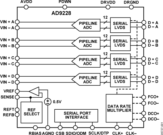
AD9228-65EBZ
Part Number : AD9228-65EBZ
Analog Devices Inc.The AD9228 is a quad, 12-bit, 40/65 MSPS analog-to-digital converter (ADC) with an on-chip sample-and-hold circuit designed for low cost, low power, small size, and ease of use. The product operates at a conversion rate of up to 65 MSPS and is optimized for outstanding dynamic performance and low power in applications where a small package size is critical. The ADC requires a single 1.8 V power supply and LVPECL-/ CMOS-/LVDS-compatible sample rate clock for full performance operation. No external reference or driver components are required for many applications. The ADC automatically multiplies the sample rate clock for the appropriate LVDS serial data rate. A data clock output (DCO) for capturing data on the output and a frame clock output (FCO) for signaling a new output byte are provided. Individual channel power-down is supported and typically consumes The ADC contains several features designed to maximize flexibility and minimize system cost, such as programmable clock and data alignment and programmable digital test pattern generation. The available digital test patterns include built-in deterministic and pseudorandom patterns, along with custom user-defined test patterns entered via the serial port interface (SPI). The AD9228 is available in an RoHS compliant, 48-lead LFCSP. It is specified over the industrial temperature range of −40°C to +85°C.PRODUCT HIGHLIGHTSSmall Footprint. Four ADCs are contained in a small, space-saving package. Low power of 119 mW/channel at 65 MSPS. Ease of Use. A data clock output (DCO) is provided that operates at frequencies of up to 390 MHz and supports double data rate (DDR) operation.User Flexibility. The SPI control offers a wide range of flexible features to meet specific system requirements. Pin-Compatible Family. This includes the AD9287 (8-bit), AD9219 (10-bit), and AD9259 (14-bit). APPLICATIONSMedical imaging and nondestructive ultrasound Portable ultrasound and digital beam-forming systemsQuadrature radio receivers Diversity radio receivers Tape drives Optical networking Test equipment

AD9552/PCBZ
Part Number : AD9552/PCBZ
Analog Devices Inc.The AD9552 is a fractional-N phase locked loop (PLL) based clock generator designed specifically to replace high frequency crystal oscillators and resonators. The device employs a sigma-delta (Σ-Δ) modulator (SDM) to accommodate fractional frequency synthesis. The user supplies an input reference signal by connecting a single-ended clock signal directly to the REF pin or by connecting a crystal resonator across the XTAL pins.The AD9552 is pin programmable, providing one of 64 standard output frequencies based on one of eight common input frequencies. The device also has a 3-wire SPI interface, enabling the user to program custom input-to-output frequency ratios.The AD9552 relies on an external capacitor to complete the loop filter of the PLL. The output is compatible with LVPECL, LVDS, or single-ended CMOS logic levels, although the AD9552 is implemented in a strictly CMOS process.The AD9552 is specified to operate over the extended industrial temperature range of −40°C to +85°C.APPLICATIONS Cost effective replacement of high frequency VCXO, OCXO, and SAW resonators Extremely flexible frequency translation with low jitter for SONET/SDH (including FEC) , 10 Gb Ethernet, Fibre Channel, and DRFI/DOCSIS High-definition video frequency translation Wireless infrastructure Test and measurement (including handheld devices)

AD9714BCPZ
Part Number : AD9714BCPZ
Analog Devices Inc.The AD9714/AD9715/AD9716/AD9717 are pin-compatible, dual, 8-/10-/12-/14-bit, low power digital-to-analog converters (DACs) that provide a sample rate of 125 MSPS. These TxDAC® converters are optimized for the transmit signal path of communication systems. All the devices share the same interface, package, and pinout, providing an upward or downward component selection path based on performance, resolution, and cost.The AD9714/AD9715/AD9716/AD9717 offer exceptional ac and dc performance and support update rates up to 125 MSPS.The flexible power supply operating range of 1.8 V to 3.3 V and low power dissipation of the AD9714/AD9715/AD9716/AD9717 make them well-suited for portable and low power applications.PRODUCT HIGHLIGHTS Low Power. DACs operate on a single 1.8 V to 3.3 V supply; total power consumption reduces to 35 mW at 125 MSPS with a 1.8 V supply. Sleep and power-down modes are provided for low power idle periods. LVCMOS Clock Input. High speed, single-ended LVCMOS clock input supports a 125 MSPS conversion rate. Easy Interfacing to Other Components. Adjustable output common mode from 0 V to 1.2 V allows easy interfacing to other components that accept common- mode levels greater than 0 V. APPLICATIONS Wireless infrastructures Picocell, femtocell base stations Medical instrumentation Ultrasound transducer excitation Portable instrumentation Signal generators, arbitrary waveform generators
AD9717-DPG2-EBZ
Part Number : AD9717-DPG2-EBZ
Analog Devices Inc.The AD9714 / AD9715 / AD9716 / AD9717 are pin-compatible, dual, 8-/10-/12-/14-bit, low power digital-to-analog converters (DACs) that provide a sample rate of 125 MSPS. These TxDAC® converters are optimized for the transmit signal path of communication systems. All the devices share the same interface, package, and pinout, providing an upward or downward component selection path based on performance, resolution, and cost.The AD9714 / AD9715 / AD9716 / AD9717 offer exceptional ac and dc performance and support update rates up to 125 MSPS.The flexible power supply operating range of 1.8 V to 3.3 V and low power dissipation of the AD9714 / AD9715 / AD9716 / AD9717 make them well-suited for portable and low power applications.PRODUCT HIGHLIGHTS Low Power. DACs operate on a single 1.8 V to 3.3 V supply; total power consumption reduces to 35 mW at 125 MSPS with a 1.8 V supply. Sleep and power-down modes are provided for low power idle periods. LVCMOS Clock Input. High speed, single-ended LVCMOS clock input supports a 125 MSPS conversion rate. Easy Interfacing to Other Components. Adjustable output common mode from 0 V to 1.2 V allows easy interfacing to other components that accept common- mode levels greater than 0 V.APPLICATIONS Wireless infrastructures Picocell, femtocell base stations Medical instrumentation Ultrasound transducer excitation Portable instrumentation Signal generators, arbitrary waveform generators

ADA4062-2ARZ
Part Number : ADA4062-2ARZ
Analog Devices Inc.The ADA4062-2 and ADA4062-4 are dual and quad JFET-input amplifiers with industry-leading performance. They offer lower power, offset voltage, drift, and ultralow bias current. The ADA4062-2 B grade (SOIC package) features a typical low offset voltage of 0.5 mV, an offset drift of 4 μV/°C, and a bias current of 2 pA.The ADA4062 family is ideal for various applications, including process control, industrial and instrumentation equipment, active filtering, data conversion, buffering, and power control and monitoring. With a low supply current of 165 μA per amplifier, they are well suited for lower power applications.The ADA4062 family is also specified for the extended industrial temperature range of −40°C to +125°C. The ADA4062-2 is available in lead-free, 8-lead SOIC, 8-lead MSOP, and 10-lead LFCSP (1.6 mm × 1.3 mm × 0.55 mm) packages, and the ADA4062-4 is available in a lead-free, 14-lead TSSOP package.ApplicationsPower control and monitoringActive filtersIndustrial/process controlBody probe electronicsData acquisitionIntegratorsInput buffering

ADAU1446YSTZ-3A-RL
Part Number : ADAU1446YSTZ-3A-RL
Analog Devices Inc.The ADAU1442 / ADAU1445 / ADAU1446 are enhanced audio processors that allow full flexibility in routing all input and output signals. The SigmaDSP® core features full 28-bit processing (56-bit in double-precision mode), synchronous parameter loading for ensuring filter stability, and 100% code efficiency with the SigmaStudio™ tools. This DSP allows system designers to compensate for the real-world limitations of speakers, amplifiers, and listening environments, resulting in a dramatic improvement of the perceived audio quality through speaker equalization, multiband compression, limiting, and third-party branded algorithms.The flexible audio routing matrix (FARM) allows the user to multiplex inputs from multiple sources running at various sample rates to or from the SigmaDSP core. This drastically reduces the complexity of signal routing and clocking issues in the audio system. FARM includes up to eight stereo asynchronous sample rate converters (depending on the device model), Sony/Philips Digital Interconnect Format (S/PDIF) input and output, and serial (I2S) and time division multiplexing (TDM) I/Os. Any of these inputs can be routed to the SigmaDSP core or to any of the asynchronous sample rate converters (ASRCs). Similarly, any one of the output signals can be taken from the SigmaDSP core or from any of the ASRC outputs. This routing scheme, which can be modified at any time via control registers, allows for maximum system flexibility.The ADAU1442, ADAU1445, and ADAU1446 differ only in ASRC functionality and packaging. The ADAU1442 / ADAU1445 contain 16 channels of ASRCs and are packaged in TQFP packages, whereas the ADAU1446 contains no ASRCs and is packaged in an LQFP. The ADAU1442 can handle nine clock domains, the ADAU1445 can handle three clock domains, and the ADAU1446 can handle one clock domain.The ADAU1442 / ADAU1445 / ADAU1446 can be controlled in one of two operational modes: the settings of the chip can be loaded and dynamically updated through the SPI/I2C® port, or the DSP can self-boot from an external EEPROM in a system with no microcontroller. There is also a bank of multipurpose (MP) pins that can be used as general-purpose digital I/Os or as inputs to the 4-channel auxiliary control ADC.The ADAU1442 / ADAU1445 / ADAU1446 are supported by the SigmaStudio graphical development environment. This software includes audio processing blocks such as FIR and IIR filters, dynamics processors, mixers, low level DSP functions, and third-party algorithms for fast development of custom signal flows.APPLICATIONS Automotive audio processing Head units Navigation systems Rear-seat entertainment systems DSP amplifiers (sound system amplifiers) Commercial audio processing

ADCLK914/PCBZ
Part Number : ADCLK914/PCBZ
Analog Devices Inc.The ADCLK914 is an ultrafast clock/data buffer fabricated onthe Analog Devices, Inc., proprietary, complementary bipolar(XFCB-3) silicon-germanium (SiGe) process. The ADCLK914features high voltage differential signaling (HVDS) outputssuitable for driving the latest Analog Devices high speed digitalto-analogconverters (DACs). The ADCLK914 has a single,differential open-collector output.The ADCLK914 buffer operates up to 7.5 GHz with a 160 pspropagation delay and adds only 110 fs random jitter (RJ).The input has a center tapped, 100 Ω, on-chip terminationresistor and accepts LVPECL, CML, CMOS, LVTTL, or LVDS(ac-coupled only). A VREF pin is available for biasing ac-coupledinputs.The HVDS output stage is designed to directly drive 1.9 V eachside into 50 Ω terminated to VCC for a total differential outputswing of 3.8 V.The ADCLK914 is available in a 16-lead LFCSP. It is specifiedfor operation over the extended industrial temperature range of−40°C to +125°C.Applications Clock and data signal restoration High speed converter clocking Broadband communications Cellular infrastructure High speed line receivers ATE and high performance instrumentation Level shifting Threshold detection

ADF4350BCPZ-RL
Part Number : ADF4350BCPZ-RL
Analog Devices Inc.The ADF4350 allows implementation of fractional-N orinteger-N phase-locked loop (PLL) frequency synthesizersif used with an external loop filter and external referencefrequency.The ADF4350 has an integrated voltage controlled oscillator(VCO) with a fundamental output frequency ranging from2200 MHz to 4400 MHz. In addition, divide-by-1/2/4/8 or 16circuits allow the user to generate RF output frequencies as lowas 137.5 MHz. For applications that require isolation, the RFoutput stage can be muted. The mute function is both pin- andsoftware-controllable. An auxiliary RF output is also available,which can be powered down if not in use.Control of all the on-chip registers is through a simple 3-wireinterface. The device operates with a power supply rangingfrom 3.0 V to 3.6 V and can be powered down when not in use.Applications Wireless infrastructure (W-CDMA, TD-SCDMA, WiMAX, GSM, PCS, DCS, DECT) Test equipment Wireless LANs, CATV equipment Clock generation

ADM1066ASUZ
Part Number : ADM1066ASUZ
Analog Devices Inc.The ADM1066 Super Sequencer® is a configurable supervisory/ sequencing device that offers a single-chip solution for supply monitoring and sequencing in multiple-supply systems. In addition to these functions, the ADM1066 integrates a 12-bit ADC and six 8-bit voltage output DACs. These circuits can be used to implement a closed-loop margining system that enables supply adjustment by altering either the feedback node or reference of a dc-to-dc converter using the DAC outputs. Supply margining can be performed with a minimum of external components. The margining loop can be used for in-circuit testing of a board during production (for example, to verify board functionality at −5% of nominal supplies), or it can be used dynamically to accurately control the output voltage of a dc-to-dc converter.APPLICATIONS Central office systems Servers/routers Multivoltage system line cards DSP/FPGA supply sequencing In-circuit testing of margined supplies

ADM1491EBRZ
Part Number : ADM1491EBRZ
Analog Devices Inc.The ADM1490E / ADM1491E are RS-485 transceivers with ±8 kV ESD protection and is suitable for high speed, full-duplex communication on multipoint transmission lines. In particular, the ADM1491E is designed for use in motor control applications requiring communications at data rates up to 16 Mbps.The ADM1491E is designed for balanced transmission lines and complies with TIA/EIA-485-A-98. The device has a 12 kΩ receiver input impedance for unit load RS-485 operation allowing up to 32 nodes on the bus.The differential transmitter outputs and receiver inputs feature electrostatic discharge circuitry that provides protection to ±8 kV using the human body model (HBM).The ADM1491E operates from a single 5 V power supply. Excessive power dissipation caused by bus contention or output shorting is prevented by short-circuit protection and thermal circuitry.Short-circuit protection circuits limit the maximum output current to ±250 mA during fault conditions. A thermal shutdown circuit senses if the die temperature rises above 150°C and forces the driver outputs into a high impedance state under this condition.The receiver of the ADM1491E contains a fail-safe feature that results in a logic high output state if the inputs are unconnected (floating).The ADM1491E features extremely fast and closely matched switching times. Minimal driver propagation delays permit transmission at data rates up to 16 Mbps while low skew minimizes EMI interference.The ADM1491E is fully specified over the commercial and industrial temperature ranges and is available in two packages: a narrow-body 14-lead SOIC and a 10-lead MSOP.APPLICATIONS RS-485/RS-422 interfaces Industrial field networks High data rate motor control Multipoint data transmission systems Single-ended to differential signal conversion

ADM2482EBRWZ
Part Number : ADM2482EBRWZ
Analog Devices Inc.The ADM2482E/ADM2487E are isolated data transceivers with ±15 kV ESD protection and are suitable for high speed, half-duplex or full-duplex communication on multipoint transmission lines. For half-duplex operation, the transmitter outputs and receiver inputs share the same transmission line. Transmitter Output Pin Y is linked externally to Receiver Input Pin A, and Transmitter Output Pin Z to Receiver Input Pin B. The parts are designed for balanced transmission lines and comply with TIA/EIA- 485-A-98 and ISO 8482:1987(E).The devices employ the Analog Devices, Inc., iCoupler® technology to combine a 3-channel isolator, a three-state differential line driver, and a differential input receiver into a single package. An on-chip oscillator outputs a pair of square waveforms that drive an external transformer to provide isolated power. The logic side of the device can be powered with either a 5 V or a 3.3 V supply, and the bus side is powered with an isolated 3.3 V supply.The ADM2482E/ADM2487E driver has an active high enable, and the receiver has an active low enable. The driver output enters a high impedance state when the driver enable signal is low. The receiver output enters a high impedance state when the receiver enable signal is high.The device has current-limiting and thermal shutdown features to protect against output short circuits and situations where bus contention might cause excessive power dissipation. The part is fully specified over the industrial temperature range of −40°C to +85°C and is available in a 16-lead, wide-body SOIC package.Applications Isolated RS-485/RS-422 interfaces Industrial field networks Multipoint data transmission systems

ADM2484EBRWZ
Part Number : ADM2484EBRWZ
Analog Devices Inc.The ADM2484E is an isolated data transceiver with ±15 kVESD protection suitable for high speed, half- or full-duplex communication on multipoint transmission lines. For half-duplex operation, the transmitter outputs and receiver inputs share the same transmission line. Transmitter Output Pin Y links externally to Receiver Input Pin A, and Transmitter Output Pin Z links externally to Receiver Input Pin B.Designed for balanced transmission lines, the ADM2484Ecomplies with ANSI TIA/EIA RS-485-A-1998 and ISO 8482: 1987(E). The device employs Analog Devices, Inc., iCoupler® technology to combine a 3-channel isolator, a three-state differential line driver, and a differential input receiver into a single package.The differential transmitter outputs and receiver inputs featureelectrostatic discharge circuitry that provides protection up to ±15 kV using the human body model (HBM). The logic side of the device can be powered with either a 5 V or a 3.3 V supply, whereas the bus side requires an isolated 3.3 V supply.The device has current-limiting and thermal shutdown featuresto protect against output short circuits and situations where buscontention causes excessive power dissipation.Applications Isolated RS-485/RS-422 interfaces Industrial field networks INTERBUS Multipoint data transmission systems

ADR03BRZ
Part Number : ADR03BRZ
Analog Devices Inc.The ADR01, ADR02, ADR03, and ADR06 are precision 10.0 V, 5.0 V, 2.5 V, and 3.0 V, respectively, band gap voltage references featuring high accuracy, high stability, and low power consumption. The devices are housed in tiny, 5-lead SC70 and TSOT packages, as well as in 8-lead SOIC version. The SOIC version of the ADR01, ADR02, and ADR03 are drop-in replacements1 to the industry-standard REF01, REF02, and REF03. The small footprint and wide operating range make the ADR01, ADR02, ADR03, and ADR06 references ideally suited for general-purpose and space-constrained applications.With an external buffer and a simple resistor network, the TEMP pin can be used for temperature sensing and approximation. A TRIM pin is provided on the devices for fine adjustment of the output voltage.The ADR01, ADR02, ADR03, and ADR06 are compact, low drift voltage references that provide a stable output voltage from a wide supply voltage range. The devices are available in 5-lead SC70 and TSOT packages and an 8-lead SOIC package with A, B, and C grade selections. All devices are specified over the extended industrial (−40°C to +125°C) temperature range. The ADR01, ADR02, ADR03, and ADR06 A grade in 8-lead SOIC are qualified for automotive applications.Applications Precision data acquisition systems High resolution converters Industrial process control systems Precision instruments Auto battery monitoring PCMCIA cards1 ADR01, ADR02, and ADR03 are component level compatible with REF01, REF02, and REF03, respectively. No guarantees for system level compatibility are implied. SOIC versions of ADR01, ADR02, and ADR03 are pin-to-pin compatible with the 8-lead SOIC versions of the REF01, REF02, REF03, respectively, with the additional temperature monitoring function.

ADR423ARMZ-REEL7
Part Number : ADR423ARMZ-REEL7
Analog Devices Inc. he ADR42x are a series of ultraprecision, second generation eXtra implanted junction FET (XFET) voltage references featuring low noise, high accuracy, and excellent long-term stability in SOIC and MSOP footprints.Patented temperature drift curvature correction technique and XFET technology minimize nonlinearity of the voltage change with temperature. The XFET architecture offers superior accuracy and thermal hysteresis to the band gap references. It also operates at lower power and lower supply headroom than the buried Zener references.The superb noise and the stable and accurate characteristics of the ADR42x make them ideal for precision conversion applications such as optical networks and medical equipment. The ADR42x trim terminal can also be used to adjust the out-put voltage over a ±0.5% range without compromising any other performance. The ADR42x series voltage references offer two electrical grades and are specified over the extended industrial temperature range of −40°C to +125°C. Devices have 8-lead SOIC or 30% smaller, 8-lead MSOP packages.APPLICATIONS Precision data acquisition systems High resolution converters Battery-powered instrumentation Portable medical instruments Industrial process control systems Precision instruments Optical network control circuits

ADR443ARMZ
Part Number : ADR443ARMZ
Analog Devices Inc.The ADR440/ADR441/ADR443/ADR444/ADR445 series is a family of XFET® voltage references featuring ultralow noise, high accuracy, and low temperature drift performance. Using Analog Devices, Inc., patented temperature drift curvature correction and XFET (eXtra implanted junction FET) technology, voltage change vs. temperature nonlinearity in the ADR440/ADR441/ADR443/ADR444/ADR445 is greatly minimized.The XFET references offer better noise performance than buried Zener references, and XFET references operate off low supply voltage headroom (500 mV). This combination of features makes the ADR440/ADR441/ADR443/ADR444/ADR445 family ideally suited for precision signal conversion applications in high-end data acquisition systems, optical networks, and medical applications.The ADR440/ADR441/ADR443/ADR444/ADR445 family has the capability to source up to 10 mA of output current and sink up to −5 mA. It also comes with a trim terminal to adjust the output voltage over a 0.5% range without compromising performance.The ADR440/ADR441/ADR443/ADR444/ADR445 family is available in 8-lead MSOP and narrow SOIC packages and offered in two electrical grades. All versions are specified over the extended industrial temperature range of −40°C to +125°C.Applications Precision data acquisition systems High resolution data converters Battery-powered instrumentation Portable medical instruments Industrial process control systems Precision instruments Optical control circuits
ADR444ARMZ
Part Number : ADR444ARMZ
Analog Devices Inc.The ADR440/ADR441/ADR443/ADR444/ADR445 series is a family of XFET® voltage references featuring ultralow noise, high accuracy, and low temperature drift performance. Using Analog Devices, Inc., patented temperature drift curvature correction and XFET (eXtra implanted junction FET) technology, voltage change vs. temperature nonlinearity in the ADR440/ADR441/ADR443/ADR444/ADR445 is greatly minimized.The XFET references offer better noise performance than buried Zener references, and XFET references operate off low supply voltage headroom (500 mV). This combination of features makes the ADR440/ADR441/ADR443/ADR444/ADR445 family ideally suited for precision signal conversion applications in high-end data acquisition systems, optical networks, and medical applications.The ADR440/ADR441/ADR443/ADR444/ADR445 family has the capability to source up to 10 mA of output current and sink up to −5 mA. It also comes with a trim terminal to adjust the output voltage over a 0.5% range without compromising performance.The ADR440/ADR441/ADR443/ADR444/ADR445 family is available in 8-lead MSOP and narrow SOIC packages and offered in two electrical grades. All versions are specified over the extended industrial temperature range of −40°C to +125°C.Applications Precision data acquisition systems High resolution data converters Battery-powered instrumentation Portable medical instruments Industrial process control systems Precision instruments Optical control circuits


