AD627BNZ
Part Number : AD627BNZ
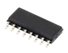
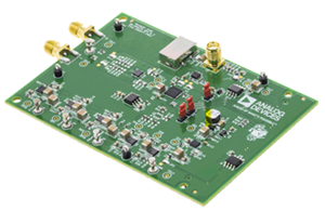
Analog Devices Inc.The AD627 is an integrated, micropower instrumentation amplifier that delivers rail-to-rail output swing on single and dual (+2.2 V to ±18 V) supplies. The AD627 provides excellent ac and dc specifications while operating at only 85 μA maximum.The AD627 offers superior flexibility by allowing the user to set the gain of the device with a single external resistor while con-forming to the 8-lead industry-standard pinout configuration. With no external resistor, the AD627 is configured for a gain of 5. With an external resistor, it can be set to a gain of up to 1000.A wide supply voltage range (+2.2 V to ±18 V) and micropower current consumption make the AD627 a perfect fit for a wide range of applications. Single-supply operation, low power consumption, and rail-to-rail output swing make the AD627 ideal for battery-powered applications. Its rail-to-rail output stage maximizes dynamic range when operating from low supply voltages. Dual-supply operation (±15 V) and low power consumption make the AD627 ideal for industrial applications, including 4 to 20 mA loop-powered systems.The AD627 does not compromise performance, unlike other micropower instrumentation amplifiers. Low voltage offset, offset drift, gain error, and gain drift minimize errors in the system. The AD627 also minimizes errors over frequency by providing excellent CMRR over frequency. Because the CMRR remains high up to 200 Hz, line noise and line harmonics are rejected.The AD627 provides superior performance, uses less circuit board area, and costs less than micropower discrete designs.Applications4 mA to 20 mA loop-powered applicationsLow power medical instrumentation—ECG, EEGTransducer interfacingThermocouple amplifiersIndustrial process controlsLow power data acquisitionPortable battery-powered instruments
AD7476ABKSZ-REEL7
Part Number : AD7476ABKSZ-REEL7
Analog Devices Inc.The AD7476A / AD7477A / AD7478A are 12-bit, 10-bit, and 8-bithigh speed, low power, successive-approximation analog-to-digitalconverters (ADCs), respectively. The parts operate froma single 2.35 V to 5.25 V power supply and feature throughputrates up to 1 MSPS. The parts contain a low noise, widebandwidth track-and-hold amplifier that can handle inputfrequencies in excess of 13 MHz. The conversion process anddata acquisition are controlled using CS and the serial clock,allowing the devices to interface with microprocessors or DSPs.The input signal is sampled on the falling edge of CS, and theconversion is also initiated at this point. There are no pipelinedelays associated with the parts. The AD7476A / AD7477A /AD7478A use advanced design techniques to achieve low powerdissipation at high throughput rates. The reference for the partis taken internally from VDD to allow the widest dynamic inputrange to the ADC. Thus, the analog input range for the part is0 V to VDD. The conversion rate is determined by the SCLK.PRODUCT HIGHLIGHTS First 12-/10-/8-bit ADCs in a SC70 package. High throughput with low power consumption. Flexible power/serial clock speed management. The conversion rate is determined by the serial clock, allowing the conversion time to be reduced through the serial clock speed increase. This allows the average power consumption to be reduced when a power-down mode is used while not converting. The parts also feature a power-down mode to maximize power efficiency at lower throughput rates. Current consumption is 1 µA maximum and 50 nA typically when in power-down mode. Reference derived from the power supply. No pipeline delay. The parts feature a standard successive approximation ADC with accurate control of the sampling instant via a CS input and once-off conversion control.APPLICATIONS Battery-powered systems Personal digital assistants Medical instruments Mobile communications Instrumentation and control systems Data acquisition systems High speed modems Optical sensors
AD7476SRTZ-REEL
Part Number : AD7476SRTZ-REEL
Analog Devices Inc.The AD7476/AD7477/AD7478 are, respectively, 12-bit, 10-bit, and 8-bit, high speed, low power, successive approximation ADCs. The parts operate from a single 2.35 V to 5.25 V power supply and feature throughput rates up to 1 MSPS. Each part contains a low noise, wide bandwidth track-and-hold amplifier that can handle input frequencies in excess of 6 MHz.The conversion process and data acquisition are controlled using CS the serial clock, allowing the devices to interface with microprocessors or DSPs. The input signal is sampled on the falling edge of CS and the conversion is initiated at this point. There are no pipeline delays associated with these parts.The AD7476/AD7477/AD7478 use advanced design techniques to achieve very low power dissipation at high throughput rates. The reference for the parts is taken internally from VDD. This allows the widest dynamic input range to the ADC. Thus, the analog input range for the parts are 0 V to VDD. The conversion rate is determined by the SCLK.
AD7612BSTZ
Part Number : AD7612BSTZ
Analog Devices Inc.The AD7612 is a 16-bit charge redistribution successive approximation register (SAR), architecture analog-to-digital converter (ADC) fabricated on Analog Devices, Inc.'s iCMOS high voltage process. The device is configured through hardware or via a dedicated write only serial configuration port for input range and operating mode. The AD7612 contains a high speed 16-bit sampling ADC, an internal conversion clock, an internal reference (and buffer), error correction circuits, and both serial and parallel system interface ports. A falling edge on CNVST samples the analog input on IN+ with respect to a ground sense, IN–. The AD7612 features four different analog input ranges and three different sampling modes: warp mode for the fastest throughput, normal mode for the fastest asynchronous throughput, and impulse mode where power consumption is scaled linearly with throughput. Operation is specified from −40°C to +85°C. ol { margin-top:0px; margin-right:0px; margin-bottom:0px; margin-left:25px; padding-top:0px; padding-right:0px; padding-bottom:10px; padding-left:0px;} li { padding-top:0px; padding-right:0px; padding-bottom:5px; padding-left:0px; margin-top:0px; margin-right:0px; margin-bottom:0px; margin-left:0px;}Product Highlights Programmable input range and mode selection. Pins or serial port for selecting input range/mode select. Fast throughput. In warp mode, the AD7612 is 750 kSPS. Superior Linearity. No missing 16-bit code. ±1.5 LSB max INL. Internal Reference. 5 V internal reference with a typical drift of ±3 ppm/°C and an on-chip temperature sensor. Serial or Parallel Interface. Versatile parallel (16- or 8-bit bus) or 2-wire serial interface arrangement compatible with 3.3 V or 5 V logic.Applications Process control Medical instruments High speed data acquisition Digital signal processing Instrumentation Spectrum analysis ATE
AD7691SRMZ-EP-RL7
Part Number : AD7691SRMZ-EP-RL7
Analog Devices Inc.The AD7691 is an 18-bit, charge redistribution, successive approximation, analog-to-digital converter (ADC) that operates from a single power supply, VDD, between 2.3 V and 5 V. It contains a low power, high speed, 18-bit sampling ADC with no missing codes, an internal conversion clock, and a versatile serial interface port. On the CNV rising edge, it samples the voltage difference between the IN+ and IN− pins. The voltages on these pins usually swing in opposite phase between 0 V and REF. The reference voltage, REF, is applied externally and can be set up to the supply voltage. The part’s power scales linearly with throughput.The SPI-compatible serial interface also features the ability, using the SDI input, to daisy-chain several ADCs on a single 3-wire bus and provides an optional busy indicator. It is compatible with 1.8 V, 2.5 V, 3 V, or 5 V logic, using the separate VIO supply.The AD7691 is housed in a 10-lead MSOP or a 10-lead QFN (LFCSP) with operation specified from −40°C to +85°C.Applications Battery-powered equipment Data acquisitions Seismic data acquisition systems Instrumentation Medical instruments
AD7814ARMZ-REEL7
Part Number : AD7814ARMZ-REEL7
Analog Devices Inc.The AD7814 is a complete temperature monitoring system in aSOT-23 package or 8-lead MSOP package. It contains a bandgap temperature sensor and 10-bit ADC to monitor and digitizethe temperature reading to a resolution of 0.25°CThe AD7814 has a flexible serial interface that allows easy interfacing to most microcontrollers. The interface is compatiblewith SPI®, QSPI™, and MICROWIRE™ protocol, and is alsocompatible with DSPs. The part features a standby mode that iscontrolled via the serial interface.The AD7814’s wide supply voltage range, low supply current,and SPI-compatible interface make it ideal for a variety ofapplications, including personal computers, office equipment,and domestic appliances.PRODUCT HIGHLIGHTS The AD7814 has an on-chip temperature sensor that allows an accurate measurement of the ambient temperature. The measurable temperature range is –55°C to +125°C, with a ±2°C temperature accuracy. Supply voltage of 2.7 V to 5.5 V Space-saving 6-lead SOT-23 package and 8-lead MSOP package 10-bit temperature reading to 0.25°C resolution Standby mode that reduces the current consumption to 1 µAAPPLICATIONS Hard Disk Drives Personal Computers Electronic Test Equipment Office Equipment Domestic Appliances Process Control
AD8065ARZ-REEL7
Part Number : AD8065ARZ-REEL7
Analog Devices Inc.The AD8065/AD80661 FastFET™ amplifiers are voltage feedback amplifiers with FET inputs offering high performance and ease of use. The AD8065 is a single amplifier, and the AD8066 is a dual amplifier. These amplifiers are developed in the Analog Devices, Inc. proprietary XFCB process and allow exceptionally low noise operation (7.0 nV/√Hz and 0.6 fA/√Hz) as well as very high input impedance.With a wide supply voltage range from 5 V to 24 V, the ability to operate on single supplies, and a bandwidth of 145 MHz, the AD8065/AD8066 are designed to work in a variety of applications. For added versatility, the amplifiers also contain rail-to-rail outputs.Despite the low cost, the amplifiers provide excellent overall performance. The differential gain and phase errors of 0.02% and 0.02°, respectively, along with 0.1 dB flatness out to 7 MHz, make these amplifiers ideal for video applications. Additionally, they offer a high slew rate of 180 V/µs, excellent distortion (SFDR of −88 dBc @ 1 MHz), extremely high common-mode rejection of −100 dB, and a low input offset voltage of 1.5 mV maximum under warmed up conditions. The AD8065/AD8066 operate using only a 6.4 mA/amplifier typical supply current and are capable of delivering up to 30 mA of load current.The AD8065/AD8066 are high performance, high speed, FET input amplifiers available in small packages: SOIC-8, MSOP-8, and SOT-23-5. They are rated to work over the industrial temperature range of −40°C to +85°C.The AD8065WARTZ-R7 is fully qualified for automotive applications. It is rated to operate over the extended temperature range (−40°C to +105°C), up to a maximum supply voltage range of ±5 V onlyApplications Automotive driver assistance systems Photodiode preamps Filters A/D drivers Level shifting Buffering
AD8182ARZ
Part Number : AD8182ARZ
Analog Devices Inc.The AD8180 (single) and AD8182 (dual) are high speed 2-to-1 multiplexers. They offer -3 dB signal bandwidth greater than 780 MHz along with slew rate of 750 V/µs. With better than 77 dB of crosstalk and 84 dB of isolation, they are useful in many high speed applications. The differential gain and differential phase error of 0.02% and 0.02°, along with 0.1 dB flatness beyond 100 MHz make AD8180 and AD8182 ideal for professional video multiplexing. They offer 5 ns switching time making them an excellent choice for pixel switching (picture-in-picture) while consuming only less than 3.8 mA (per 2:1 mux) on ±5 V supply voltage. Both devices offer a high speed disable feature allowing the output to be put into a high impedance state. This allows multiple outputs to be connected together for cascading stages while the 'OFF' channels do not load the output bus. They operate on voltage supplies of ±5 V and are offered in 8- and 14-lead PDIP and SOIC packages.An evaluation board is available for this product and may be ordered using the following product number: AD8180-EB and AD8182-EB. Schematic and layout for this evaluation board is contained in the product datasheet.
AD822TRZ-EP
Part Number : AD822TRZ-EP
Analog Devices Inc.The AD822 is a dual precision, low power FET input op ampthat can operate from a single supply of 5 V to 30 V or dual supplies of ±2.5 V to ±15 V. It has true single-supply capability with an input voltage range extending below the negative rail, allowing the AD822 to accommodate input signals belowground in the single-supply mode. Output voltage swing extends to within 10 mV of each rail, providing the maximumoutput dynamic range.Offset voltage of 800 μV maximum, offset voltage drift of 2 μV/°C, input bias currents below 25 pA, and low input voltage noise provide dc precision with source impedances up to a gigaohm. The 1.8 MHz unity-gain bandwidth, –93 dB THD at 10 kHz,and 3 V/μs slew rate are provided with a low supply current of 800 μA per amplifier.Applications Battery-powered precision instrumentation Photodiode preamps Active filters 12-bit to 14-bit data acquisition systems Medical instrumentation Low power references and regulatorsThe AD822-EP supports defense and aerospace applications (AQEC standard)
AD8310ARMZ-REEL7
Part Number : AD8310ARMZ-REEL7
Analog Devices Inc.The AD8310 is a complete, dc to 440 MHz demodulating logarithmic amplifier (log amp) with a very fast voltage mode output, capable of driving up to 25 mA into a grounded load in under 15 ns. It uses the progressive compression (successive detection) technique to provide a dynamic range of up to 95 dB to ±3 dB law conformance or 90 dB to a ±1 dB error bound up to 100 MHz. It is extremely stable and easy to use, requiring no significant external components. A single-supply voltage of 2.7 V to 5.5 V at 8 mA is needed, corresponding to a power consumption of only 24 mW at 3 V. A fast-acting CMOS-compatible enable pin is provided.Each of the six cascaded amplifier/limiter cells has a small-signal gain of 14.3 dB, with a −3 dB bandwidth of 900 MHz. A total of nine detector cells are used to provide a dynamic range that extends from −91 dBV (where 0 dBV is defined as the amplitude of a 1 V rms sine wave), an amplitude of about ±40 μV, up to +4 dBV (or ±2.2 V). The demodulated output is accurately scaled, with a log slope of 24 mV/dB and an intercept of −108 dBV. The scaling parameters are supply- and temperature-independent.The fully differential input offers a moderately high impedance (1 kΩ in parallel with about 1 pF). A simple network can match the input to 50 Ω and provide a power sensitivity of −78 dBm to +17 dBm. The logarithmic linearity is typically within ±0.4 dB up to 100 MHz over the central portion of the range, but it is somewhat greater at 440 MHz. There is no minimum frequency limit; the AD8310 can be used down to low audio frequencies. Special filtering features are provided to support this wide range.The output voltage runs from a noise-limited lower boundary of 400 mV to an upper limit within 200 mV of the supply voltage for light loads. The slope and intercept can be readily altered using external resistors. The output is tolerant of a wide variety of load conditions and is stable with capacitive loads of 100 pF.The AD8310 provides a unique combination of low cost, small size, low power consumption, high accuracy and stability, high dynamic range, a frequency range encompassing audio to UHF, fast response time, and good load-driving capabilities, making this product useful in numerous applications that require the reduction of a signal to its decibel equivalent.The AD8310 is available in the industrial temperature range of −40°C to +85°C in an 8-lead MSOP package.Applications Conversion of signal level to decibel form Transmitter antenna power measurement Receiver signal strength indication (RSSI) Low cost radar and sonar signal processing Network and spectrum analyzers Signal-level determination down to 20 Hz True-decibel ac mode for multimeters
AD8351ARMZ-REEL7
Part Number : AD8351ARMZ-REEL7
Analog Devices Inc.The AD8351 is a low cost differential amplifier useful in RF andIF applications up to 2.2 GHz. The voltage gain can be set fromunity to 26 dB using a single external gain resistor. The AD8351provides a nominal 150 Ω differential output impedance. Theexcellent distortion performance and low noise characteristicsof this device allow for a wide range of applications.The AD8351 is designed to satisfy the demanding performancerequirements of communications transceiver applications. Thedevice can be used as a general-purpose gain block, an ADCdriver, and a high speed data interface driver, among otherfunctions. The AD8351 can also be used as a single-ended-to-differentialamplifier with similar distortion products as in thedifferential configuration. The exceptionally good distortionperformance makes the AD8351 an ideal solution for 12-bit and14-bit IF sampling receiver designs.Fabricated in Analog Devices, Inc., high speed XFCB process,the AD8351 has high bandwidth that provides high frequencyperformance and low distortion. The quiescent current of theAD8351 is 28 mA typically. The AD8351 amplifier comes in acompact 10-lead MSOP package or in a 16-lead LFCSP package,and operates over the temperature range of −40°C to +85°C.Applications Differential ADC drivers Single-ended-to-differential conversion IF sampling receivers RF/IF gain blocks SAW filter interfacing AvailabilityOther RF / IF amplifiers products:AD8367 - 500 MHz Single Ended, Analog Controlled VGA AD8369 - 600 MHz, 45 dB Digitally Controlled Variable Gain Amplifier AD8350 - 1.0 GHz Differential Amplifier
AD8611ARZ-REEL7
Part Number : AD8611ARZ-REEL7
Analog Devices Inc.The AD8611/AD8612 are single and dual 4 ns comparators with latch function and complementary output. The latch is not functional if VCC is less than 4.3 V.Fast 4 ns propagation delay makes the AD8611/AD8612 good choices for timing circuits and line receivers. Propagation delays for rising and falling signals are closely matched and tracked over temperature. This matched delay makes the AD8611/AD8612 good choices for clock recovery because the duty cycle of the output matches the duty cycle of the input.The AD8611 has the same pinout as the LT1016 and LT1394, with lower supply current and a wider common-mode input range, which includes the negative supply rail.The AD8611/AD8612 are specified over the industrial temperature range (−40°C to +85°C). The AD8611 is available in both 8-lead MSOP and narrow 8-lead SOIC surface-mount packages. The AD8612 is available in a 14-lead TSSOP surface-mount package.Applications High speed timing Clock recovery and clock distribution Line receivers Digital communications Phase detectors High speed sampling Read channel detection PCMCIA cards Zero-crossing detector High speed analog-to-digital converter (ADC) Upgrade for LT1394 and LT1016 designs
AD9244BSTZ-65
Part Number : AD9244BSTZ-65
Analog Devices Inc.The AD9244 is a monolithic, single 5 V supply, 14-bit, 65 MSPS analog-to-digital converter with an on-chip, high performance, sample and hold amplifier and voltage reference. The AD9244 uses a multi-stage differential pipelined architecture with output error correction logic to provide 14-bit accuracy at 65 MSPS data rates and guarantees no missing codes over the full operating temperature range.The AD9244 has an on-board, programmable voltage reference. An external reference can also be chosen to suit the DC accuracy and temperature drift requirements of the application.A differential clock input is used to control all internal conversion cycles. The digital output data can be presented in straight binary or in twos complement format. An out of range (OTR) signal indicates an overflow condition, which can be used with the most significant bit to determine low or high overflow.Fabricated on an advanced CMOS process, the AD9244 is available in a 48 pin surface mount plastic package (48-LQFP) and is specified for operation over the industrial temperature range of (-40°C to +85°C).
ADF4156BCPZ-RL7
Part Number : ADF4156BCPZ-RL7
Analog Devices Inc.The ADF4156 is a 6.2 GHz fractional-N frequency synthesizer that implements local oscillators in the up-conversion and down-conversion sections of wireless receivers and transmitters. It consists of a low noise digital phase frequency detector (PFD), a precision charge pump, and a programmable reference divider. There is a ∑∆ based fractional interpolator to allow programmable fractional-N division. The INT, FRAC, and MOD registers define an overall N divider (N = (INT + (FRAC/MOD))). The RF output phase is programmable for applications that require a particular phase relationship between the output and the reference. The ADF4156 also features cycle slip reduction circuitry, leading to faster lock times without the need for modifications to the loop filter.Control of all on-chip registers is via a simple 3-wire interface. The device operates with a power supply ranging from 2.7 V to 3.3 V and can be powered down when not in use.ApplicationsCATV equipmentBase stations for mobile radio (WiMAX, GSM, PCS, DCS, SuperCell 3G, CDMA, WCDMA)Wireless handsets (GSM, PCS, DCS, CDMA, WCDMA)Wireless LANs, PMRCommunications test equipment
ADF4156BRUZ-RL7
Part Number : ADF4156BRUZ-RL7
Analog Devices Inc.The ADF4156 is a 6.2 GHz fractional-N frequency synthesizer that implements local oscillators in the up-conversion and down-conversion sections of wireless receivers and transmitters. It consists of a low noise digital phase frequency detector (PFD), a precision charge pump, and a programmable reference divider. There is a ∑∆ based fractional interpolator to allow programmable fractional-N division. The INT, FRAC, and MOD registers define an overall N divider (N = (INT + (FRAC/MOD))). The RF output phase is programmable for applications that require a particular phase relationship between the output and the reference. The ADF4156 also features cycle slip reduction circuitry, leading to faster lock times without the need for modifications to the loop filter.Control of all on-chip registers is via a simple 3-wire interface. The device operates with a power supply ranging from 2.7 V to 3.3 V and can be powered down when not in use.ApplicationsCATV equipmentBase stations for mobile radio (WiMAX, GSM, PCS, DCS, SuperCell 3G, CDMA, WCDMA)Wireless handsets (GSM, PCS, DCS, CDMA, WCDMA)Wireless LANs, PMRCommunications test equipment
ADG1206YRUZ
Part Number : ADG1206YRUZ
Analog Devices Inc.The ADG1206 and ADG1207 are monolithic iCMOS® analogmultiplexers comprising sixteen single channels and eightdifferential channels, respectively. The ADG1206 switches oneof sixteen inputs to a common output, as determined by the4-bit binary address lines A0, A1, A2, and A3. The ADG1207switches one of eight differential inputs to a common differentialoutput, as determined by the 3-bit binary address lines A0, A1,and A2. An EN input on both devices is used to enable or disablethe device. When disabled, all channels are switched off. Whenon, each channel conducts equally well in both directions andhas an input signal range that extends to the supplies.The industrial CMOS (iCMOS) modular manufacturingprocess combines high voltage complementary metal-oxide semiconductor (CMOS) and bipolar technologies. It enables thedevelopment of a wide range of high performance analog ICscapable of 33 V operation in a footprint that no other generationof high voltage devices has been able to achieve. Unlike analogICs using conventional CMOS processes, iCMOS componentscan tolerate high supply voltages while providing increasedperformance, dramatically lower power consumption, andreduced package size. The ultralow capacitance and exceptionally low charge injectionof these multiplexers make them ideal solutions for data acquisitionand sample-and-hold applications, where low glitch and fastsettling are required. There is minimumcharge injection over the entire signal range of the device.iCMOS construction also ensures ultralow power dissipation,making the devices ideally suited for portable and battery-poweredinstruments.Applications Audio and video routing Automatic test equipment Data acquisition systems Battery-powered systems Sample-and-hold systems Communication systems
ADG1234YRUZ
Part Number : ADG1234YRUZ
Analog Devices Inc.The ADG1233 and ADG1234 are monolithic iCMOS® analogswitches comprising three independently selectable single-pole,double throw SPDT switches and four independently selectableSPDT switches, respectively.All channels exhibit break-before-make switching actionpreventing momentary shorting when switching channels. AnEN input on the ADG1233 and ADG1234 enables or disablesthe device. When disabled, all channels are switched off.The iCMOS (industrial-CMOS) modular manufacturing processcombines a high voltage complementary metal-oxide semiconductor(CMOS) and bipolar technologies. It enables thedevelopment of a wide range of high performance analog ICscapable of 33 V operation in a footprint that no other generation ofhigh voltage devices has been able to achieve.Unlike analog ICs using conventional CMOS processes, iCMOScomponents can tolerate high supply voltages while providingincreased performance, dramatically lowered power consumption,and reduced package size.The ultralow capacitance and charge injection of these multiplexersmake them ideal solutions for data acquisition and sample-andholdapplications, where low glitch and fast settling are required.Fast switching speed coupled with high signal bandwidth make thedevices suitable for video signal switching. iCMOS constructionensures ultralow power dissipation, making the devices ideallysuited for portable and battery-powered instruments.Product Highlights 1.5 pF off capacitance (±15 V supply). 0.5 pC charge injection. 3 V logic-compatible digital input, VIH = 2.0 V, VIL = 0.8 V. 16-lead TSSOP, 20-lead TSSOP, and 4 mm × 4 mm LFCSP.Applications Audio and video routing Automatic test equipment Data acquisition systems Battery-powered systems Sample-and-hold systems Communication systems
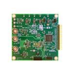
DC1908A-G
Part Number : DC1908A-G
Analog Devices Inc.Data Conversion IC Development Tools LTC2328-16 Demo Board -16-Bit, 1Msps, Si
EVAL-ADUM1441EBZ
Part Number : EVAL-ADUM1441EBZ
Analog Devices Inc.The ADuM1440/ADuM1441/ADuM1442/ADuM1445/ADuM1446/ADuM1447 are micropower, 4-channel digital isolators based on the Analog Devices, Inc., iCoupler® technology. Combining high speed, complementary metal oxide semiconductor (CMOS) and monolithic air core transformer technologies, these isolation components provide outstanding performance characteristics superior to the alternatives, such as optocoupler devices. As shown in Figure 3 in the data sheet, in standard operating mode, when ENx = 0 (internal refresh enabled), the current per channel is less than 10 μA. When ENx = 1 (internal refresh disabled), the current per channel drops to less than 1 μA.The ADuM1440/ADuM1441/ADuM1442/ADuM1445/ADuM1446/ADuM1447 family of quad 2.5 kV digital isolation devices are packaged in a small 16-lead QSOP and 20-lead SSOP, freeing almost 70% of board space compared to isolators packages in wide body SOIC packages.The devices withstand high isolation voltages and meet regulatory requirements, such as UL and CSA standards. In addition to the space savings, the ADuM1440/ADuM1441/ADuM1442/ADuM1445/ADuM1446/ADuM1447 operate with supplies as low as 2.25 V.Despite the low power consumption, all models of the ADuM1440/ADuM1441/ADuM1442/ADuM1445/ADuM1446/ADuM1447 provide low, pulse width distortion at
HMC996LP4E
Part Number : HMC996LP4E
Analog Devices Inc.The HMC996LP4E is a GaAs PHEMT MMIC analog variable gain amplifier and / or driver amplifier which operates between 5 and 12 GHz. Ideal for microwave radio applications, the amplifier provides up to 18.5 dB of gain, output P1dB of up to +23 dBm, and up to +34 dBm of output IP3 at maximum gain, while requiring only 170 mA from a +5V supply. Gain control voltage pin (Vctrl) is provided to allow variable gain control up to 22 dB. Gain flatness is excellent making the HMC996LP4E ideal for EW, ECM and radar applications. The HMC996LP4E is housed in a RoHS compliant 4 x 4 mm QFN leadless package and is compatible with high volume surface mount manufacturing.Applications Point-to-Point Radio Point-to-Multi-Point Radio EW & ECM Subsystems X-Band Radar Test Equipment & Sensors


