Manufacturer
Stock

Displaying 441 - 460 of 93400

Parts from Analog Devices Inc.

ADSP-21478BBCZ-2A

Part Number : ADSP-21478BBCZ-2A

Analog Devices Inc.
The fourth generation of SHARC® Processors now includes the low power floating point DSP products – the ADSP-21478 and ADSP-21479 and offers increased performance, hardware-based filter accelerators, audio and application-focused peripherals, and new memory configurations capable of supporting a single chip solution. All devices are pin-compatible with each other and completely code-compatible with all prior SHARC Processors. These newest members of the fourth generation SHARC Processor family are based on a single-instruction, multiple-data (SIMD) core, which supports both 32-bit fixed-point and 32-/40-bit floating-point arithmetic formats and their low power make them particularly suitable for battery powered applications or where a higher ambient operating temperature is required.The ADSP-21478 offers a very low power and high performance – 266 MHz/1596 MFLOPs – in a BGA and LQFP package within the fourth generation SHARC Processor family. This feature of power makes the ADSP-21478 particularly well suited to address the automotive audio and many industrial control segments where low power is a requirement. In addition to its high core performance, the ADSP-21478 includes additional processing blocks such as FIR, IIR, and FFT accelerators to increase the total performance of the system. There is a new feature called Variable Instruction Set Architecture (VISA) that allows the code size to be decreased by 20% to 30% and increase the memory size availability. The fourth generation DSP allows the ability to connect to external memory by providing a glueless interface to 16-bit wide SDR SDRAMs.Fourth-generation SHARC Processors also integrate application-specific peripherals designed to simplify hardware design, minimize design risks, and ultimately reduce time to market. Grouped together, and broadly named the Digital Applications Interface (DAI), these functional blocks may be connected to each other or to external pins via the software-programmable Signal Routing Unit (SRU). The SRU is an innovative architectural feature that enables complete and flexible routing amongst DAI blocks. Peripherals connected through the SRU include but are not limited to serial ports, SPI ports, S/PDIF Tx/Rx, and an 8-Channel asynchronous sample rate converter block. The fourth generation SHARC allows data from the serial ports to be directly transferred to external memory by the DMA controller. Other peripherals such as UART and Two-Wire Interface are routed through a Digital Peripheral Interface (DPI).

ADSP-BF504BCPZ-4

Part Number : ADSP-BF504BCPZ-4

Analog Devices Inc.
The BF504 is a low cost member of the Blackfin portfolio of processors. With a 400 MHz core clock speed and a unique peripheral set including two three-phase PWM units, an ADC Control Module, two SPI’s, two SPORT’s, a CAN controller, a PPI, eight general purpose counters and a Removable Storage Interface, the BF504 is feature and cost optimized for compute intensive industrial and general purpose applications that do not require external memory or executable flash. The BF504 is offered in a low cost 12 × 12mm LFCSP package in commercial and industrial temperature grades.

ADUC7023BCBZ62I-R7

Part Number : ADUC7023BCBZ62I-R7

Analog Devices Inc.
The ADuC7023 is a fully integrated, 1 MSPS, 12-bit data acquisition system, incorporating high performance multichannel ADCs, 16-bit/32-bit MCUs, and Flash/EE memory on a single chip.The ADC consists of up to 12 single-ended inputs. An additional four inputs are available but are multiplexed with the four DAC output pins. The ADC can operate in single-ended or differential input modes. The ADC input voltage is 0 V to VREF. A low drift band gap reference, temperature sensor, and voltage comparator complete the ADC peripheral set.The DAC output range is programmable to one of two voltage ranges. The DAC outputs have an enhanced feature of being able to retain their output voltage during a watchdog or software reset sequence.The devices operate from an on-chip oscillator and a PLL, generating an internal high frequency clock of 41.78 MHz. This clock is routed through a programmable clock divider from which the MCU core clock operating frequency is generated. The microcontroller core is an ARM7TDMI®, 16-bit/32-bit RISC machine that offers up to 41 MIPS peak performance. Eight kilobytes of SRAM and 62 kilobytes of nonvolatile Flash/EE memory are provided on chip. The ARM7TDMI core views all memory and registers as a single linear array.The ADuC7023 contains an advanced interrupt controller. The vectored interrupt controller (VIC) allows every interrupt to be assigned a priority level. It also supports nested interrupts to a maximum level of eight per IRQ and FIQ. When IRQ and FIQ interrupt sources are combined, a total of 16 nested interrupt levels are supported.On-chip factory firmware supports in-circuit download via the I2C serial interface port, and non-intrusive emulation is supported via the JTAG interface. These features are incorporated into a low cost QuickStart™ development system supporting this MicroConverter® family. The part contains a 16-bit PWM with five output signals.For communication purposes, the part contains 2 × I2C channels that can be individually configured for master or slave mode. An SPI interface supporting both master and slave modes is also provided.The parts operate from 2.7 V to 3.6 V and are specified over an industrial temperature range of −40°C to +125°C. The ADuC7023 is available in either a 32-lead or 40-lead LFCSP package. A 36-ball wafer level CSP package (WLCSP) is also available.Applications Optical networking Industrial control and automation systems Smart sensors, precision instrumentation Base station systems

ADUC7122BBCZ-RL

Part Number : ADUC7122BBCZ-RL

Analog Devices Inc.
The ADuC7122 is a fully integrated, 1 MSPS, 12-bit data acquisition system, incorporating high performance multichannel ADCs, 12 voltage output DACs, 16-bit/32-bit MCUs, and Flash/EE memory on a single chip. The ADC consists of up to 13 inputs. Four of these inputs can be configured as differential pairs with a Programmable Gain Amplifier on their front end providing a gain between 1 and 5. The ADC can operate in single-ended or differential input modes. The ADC input voltage is 0 V to VREF. A low drift band gap reference, temperature sensor, and supply voltage monitor complete the ADC peripheral set.The DAC output range is programmable to one of two voltage ranges. The DAC outputs have an enhanced feature of being able to retain their output voltage during a watchdog or software reset sequence.The devices operate from an on-chip oscillator and a PLL, generating an internal high frequency clock of 41.78 MHz. This clock is routed through a programmable clock divider from which the MCU core clock operating frequency is generated. The microcontroller core is an ARM7TDMI®, 16-bit/32-bit RISC machine that offers up to 41 MIPS peak performance. Eight kilobytes of SRAM and 126 kilobytes of nonvolatile Flash/EE memory are provided on chip. The ARM7TDMI core views all memory and registers as a single linear array.The ADuC7122 contains an advanced interrupt controller. The vectored interrupt controller (VIC) allows every interrupt to be assigned a priority level. It also supports nested interrupts to a maximum level of eight per IRQ and FIQ. When IRQ and FIQ interrupt sources are combined, a total of 16 nested interrupt levels are supported.On-chip factory firmware supports in-circuit download via the I2C serial interface port, while nonintrusive emulation is also supported via the JTAG interface. These features are incorporated into a low cost QuickStart™ Development System supporting this MicroConverter® family. The part contains a 16-bit PWM with six output signals.For communication purposes, the part contains 2 × I2C channels that can be individually configured for master or slave mode. An SPI¯ interface supporting both master and slave modes is also provided.The parts operate from 3.0 V to 3.6 V and are specified over atemperature range of −10°C to +95°C. The ADuC7122 is available in a 108-Ball BGA package.APPLICATIONS Optical networking, industrial control, and automation systems Smart sensors, precision instrumentation, base station systems

ADUM3472CRSZ

Part Number : ADUM3472CRSZ

Analog Devices Inc.
The ADuM3470 / ADuM3471 / ADuM3472 / ADuM3473 / ADuM3474 devicesare quad-channel, digital isolators withan integrated PWM controller and transformer driver for an isolated DC/DC converter. Based on the Analog Devices, Inc., iCoupler® technology, the DC/DC converter provides up to 2 W of regulated, isolated power at 3.3 V to 24 V from a 5.0 V input supply or from a 3.3 V supply. This eliminates the need for a separate, isolated DC/DC converter in 2 W isolated designs. The iCoupler chip-scale transformer technology is used to isolate the logic signals, and the integrated transformer driver withisolated secondary side control provides higher efficiency for the isolated DC/DC converter. The result is a small form factor, total isolation solution.The ADuM347x isolators provide four independent isolationchannels in a variety of channel configurations and data rates.APPLICATIONS RS-232/RS-422/RS-485 transceivers Industrial field bus isolation Power supply startup bias and gate drives Isolated sensor interfaces Process controls Automotive

ADUM4160BRIZ

Part Number : ADUM4160BRIZ

Analog Devices Inc.
The ADuM4160 is a USB port isolator, based on Analog Devices, Inc., iCoupler® technology. Combining high speed CMOS and monolithic air core transformer technology, these isolation components provide outstanding performance characteristics and are easily integrated with low and full speed USB-compatible peripheral devices.Many microcontrollers implement USB so that it presents only the D+ and D− lines to external pins. This is desirable in many cases because it minimizes external components and simplifies the design; however, this presents particular challenges when isolation is required. USB lines must automatically switch between actively driving D+/D−, receiving data, and allowing external resistors to set the idle state of the bus. The ADuM4160 provides mechanisms for detecting the direction of data flow and control over the state of the output buffers. Data direction is determined on a packet-by-packet basis.The ADuM4160 uses the edge detection based iCoupler technology in conjunction with internal logic to implement a transparent, easily configured, upstream facing port isolator. Isolating an upstream facing port provides several advantages in simplicity, power management, and robust operation.The isolator has propagation delay comparable to that of a standard hub and cable. It operates with the supply voltage on either side ranging from 3.1 V to 5.5 V, allowing connection directly to VBUS by internally regulating the voltage to the signaling level. The ADuM4160 provides isolated control of the pull-up resistor to allow the peripheral to control connection timing. The device has a low idle current; a suspend mode is not required.APPLICATIONS USB peripheral isolation Isolated USB hub Medical applications

ADUM4401BRIZ

Part Number : ADUM4401BRIZ

Analog Devices Inc.
The ADuM440x are 4-channel digital isolators based on the Analog Devices, Inc., iCoupler® technology. Combining high speed CMOS and monolithic air core transformer technology, these isolation components provide outstanding performance characteristics that are superior to the alternatives, such as optocoupler devices and other integrated couplers.The ADuM440x isolators provide four independent isolation channels in a variety of channel configurations and data rates (see the Ordering Guide). All models operate with the supply voltage on either side ranging from 3.0 V to 5.5 V, providing compatibility with lower voltage systems as well as enabling a voltage translation functionality across the isolation barrier. The ADuM440x isolators have a patented refresh feature that ensures dc correctness in the absence of input logic transitions and during power-up/power-down conditions.This family of isolators, like many Analog Devices isolators, offers very low power consumption, consuming one-tenth to one-sixth the power of comparable isolators at comparable data rates up to 10 Mbps. All models of the ADuM440x provide low pulse width distortion (

ADXL312ACPZ-RL

Part Number : ADXL312ACPZ-RL

Analog Devices Inc.
The ADXL312 is a small, thin, low power, 3-axis accelerometer with high resolution (13-bit) measurement up to ±12 g. Digital output data is formatted as 16-bit twos complement and is accessible through either a serial port interface (SPI) (3- or 4-wire) or I2C digital interface.The ADXL312 is well suited for car alarm or black box applications. It measures the static acceleration of gravity in tilt-sensing applications, as well as dynamic acceleration resulting from motion or shock. Its high resolution (2.9 mg/LSB) enables resolution of inclination changes of as little as 0.25°. A built-in FIFO facilitates using oversampling techniques to improve resolution to as little as 0.05° of inclination.Several special sensing functions are provided. Activity and inactivity sensing detects the presence or absence of motion and whether the acceleration on any axis exceeds a user-set level. These functions can be mapped to interrupt output pins. An integrated 32 level FIFO can be used to store data to minimize host processor intervention.Low power modes enable intelligent motion-based power management with threshold sensing and active acceleration measurement at extremely low power dissipation.The ADXL312 is supplied in a small, thin 5 mm × 5 mm × 1.45 mm, 32-lead, LFCSP package.APPLICATIONS Car alarm Hill start aid (HSA) Electronic parking brake Data recorder (black box)

DC1367A

Part Number : DC1367A

Analog Devices Inc.
The LTM4615 is a complete 4A dual output switching mode DC/DC power supply plus an additional 1.5A VLDO (very low dropout) linear regulator. Included in the package are the switching controllers, power FETs, inductors, a 1.5A regulator and all support components. The dual 4A DC/DC converters operate over an input voltage range of 2.375V to 5.5V, and the VLDO operates from a 1.14V to 3.5V input. The LTM4615 supports output voltages ranging from 0.8V to 5V for the DC/DC converters, and 0.4V to 2.6V for the VLDO. The three regulator output voltages are set by a single resistor for each output. Only bulk input and output capacitors are needed to complete the design.The low profile package (2.82mm) enables utilization of unused space on the bottom of PC boards for high density point of load regulation. High switching frequency and a current mode architecture enables a very fast transient response to line and load changes without sacrificing stability. The device supports output voltage tracking for supply rail sequencing. Additional features include overvoltage protection, foldback overcurrent protection, thermal shutdown and programmable soft-start. The power module is offered in a space saving and thermally enhanced 15mm × 15mm × 2.82mm LGA package. The LTM4615 is Pb-free and RoHS compliant.Applications Telecom and Networking Equipment Industrial Power Systems Low Noise Applications FPGA, SERDES Power

DC1500A-A

Part Number : DC1500A-A

Analog Devices Inc.
The LTC2393-16 is a low noise, high speed 16-bit successive approximation register (SAR) ADC. Operating from a single 5V supply, the LTC2393-16 supports a large ±4.096V fully differential input range, making it ideal for high performance applications which require maximum dynamic range. The LTC2393-16 achieves ±2LSB INL max, no missing codes at 16-bits and 94.2dB SNR (typ). The LTC2393-16 includes a precision internal reference with a guaranteed 0.5% initial accuracy and a ±20ppm/°C (max) temperature coefficient. Fast 1Msps throughput with no cycle latency in both parallel and serial interface modes makes the LTC2393-16 ideally suited for a wide variety of high speed applications. An internal oscillator sets the conversion time, easing external timing considerations. The LTC2393-16 dissipates only 140mW at 1Msps, while both nap and sleep power-down modes are provided to further reduce power during inactive periods.Applications Medical Imaging High Speed Data Acquisition Digital Signal Processing Industrial Process Control Instrumentation ATE

DC1532A-G

Part Number : DC1532A-G

Analog Devices Inc.
The LTC2268-12/LTC2267-12/LTC2266-12 are 2-channel, simultaneous sampling 12-bit A/D converters designed for digitizing high frequency, wide dynamic range signals. They are perfect for demanding communications applications with AC performance that includes 70.6dB SNR and 88dB spurious free dynamic range (SFDR). Ultralow jitter of 0.15psRMS allows undersampling of IF frequencies with excellent noise performance.DC specs include ±0.3LSB INL (typ), ±0.1LSB DNL (typ) and no missing codes over temperature. The transition noise is a low 0.3LSBRMS.The digital outputs are serial LVDS to minimize the number of data lines. Each channel outputs two bits at a time (2-lane mode). At lower sampling rates there is a one bit per channel option (1-lane mode). The LVDS drivers have optional internal termination and adjustable output levels to ensure clean signal integrity.The ENC+ and ENC– inputs may be driven differentially or single-ended with a sine wave, PECL, LVDS, TTL, or CMOS inputs. An internal clock duty cycle stabilizer allows high performance at full speed for a wide range of clock duty cycles.   Bits LTC2268-12 12 LTC2268-14 14 Applications Communications Cellular Base Stations Software Defined Radios Portable Medical Imaging Multichannel Data Acquisition Nondestructive Testing

DC1593A-A

Part Number : DC1593A-A

Analog Devices Inc.
The LTC2635 is a family of quad 12-, 10-, and 8-bit voltage-output DACs with an integrated, high-accuracy, low-drift reference in a 16-pin QFN or a 10-lead MSOP package. It has rail-to-rail output buffers and is guaranteed monotonic. The LTC2635-L has a full-scale output of 2.5V, and operates from a single 2.7V to 5.5V supply. The LTC2635-H has a full-scale output of 4.096V, and operates from a 4.5V to 5.5V supply. Each DAC can also operate with an external reference, which sets the fullscale output to the external reference voltage. These DACs communicate via a 2-wire I2C-compatible serial interface. The LTC2635 operates in both the standard mode (clock rate of 100kHz) and the fast mode (clock rate of 400kHz). The LTC2635 incorporates a power-on reset circuit. Options are available for reset to zero-scale, reset to mid-scale in internal reference mode, reset to mid-scale in external reference mode, or reset with all DAC outputs in a high-impedance state after power-up.Applications Mobile Communications Process Control and Industrial Automation Power Supply Margining Portable Equipment Automotive

DC1593A-D

Part Number : DC1593A-D

Analog Devices Inc.
The LTC2635 is a family of quad 12-, 10-, and 8-bit voltage-output DACs with an integrated, high-accuracy, low-drift reference in a 16-pin QFN or a 10-lead MSOP package. It has rail-to-rail output buffers and is guaranteed monotonic. The LTC2635-L has a full-scale output of 2.5V, and operates from a single 2.7V to 5.5V supply. The LTC2635-H has a full-scale output of 4.096V, and operates from a 4.5V to 5.5V supply. Each DAC can also operate with an external reference, which sets the fullscale output to the external reference voltage. These DACs communicate via a 2-wire I2C-compatible serial interface. The LTC2635 operates in both the standard mode (clock rate of 100kHz) and the fast mode (clock rate of 400kHz). The LTC2635 incorporates a power-on reset circuit. Options are available for reset to zero-scale, reset to mid-scale in internal reference mode, reset to mid-scale in external reference mode, or reset with all DAC outputs in a high-impedance state after power-up.Applications Mobile Communications Process Control and Industrial Automation Power Supply Margining Portable Equipment Automotive

DC1684A-B

Part Number : DC1684A-B

Analog Devices Inc.
The LTC2752 is a dual 16-bit multiplying serial-input, current-output digital-to-analog converter. It operates from a single 3V to 5V supply and is guaranteed monotonic over temperature. The LTC2752A provides full 16-bit performance (±1LSB INL and DNL, max) over temperature without any adjustments. This SoftSpan™ DAC offers six output ranges (up to ±10V) that can be programmed through the 3-wire SPI serial interface, or pinstrapped for operation in a single range. Any on-chip register (including DAC output-range settings) can be read for verification in just one instruction cycle; and if you change register content, the altered register will be automatically read back during the next instruction cycle. Voltage-controlled offset and gain adjustments are also provided; and the power-on reset circuit and CLR pin both reset the DAC outputs to 0V regardless of output range.Applications High Resolution Offset and Gain Adjustment Process Control and Industrial Automation Automatic Test Equipment Data Acquisition Systems

DC1703A-A

Part Number : DC1703A-A

Analog Devices Inc.
The LTC2655 is a family of Quad I2C 16-/12-Bit Rail-to-Rail DACs with integrated 10ppm/°C max reference. The DACs have built-in high performance, rail-to-rail, output buffers and are guaranteed monotonic. The LTC2655-L has a full-scale output of 2.5V with the integrated reference and operates from a single 2.7V to 5.5V supply. The LTC2655-H has a full-scale output of 4.096V with the integrated reference and operates from a 4.5V to 5.5V supply. Each DAC can also operate with an external reference, which sets the full-scale output to 2 times the external reference voltage.The parts use the 2-wire I2C compatible serial interface. The LTC2655 operates in both the standard mode (maximum clock rate of 100kHz) and the fast mode (maximum clock rate of 400kHz). The LTC2655 incorporates a power-on reset circuit that is controlled by the PORSEL pin. If PORSEL is tied to GND the DACs power-on reset to zero-scale. If PORSEL is tied to VCC, the DACs power-on reset to mid-scale.Applications Mobile Communications Process Control and Industrial Automation Instrumentation Automatic Test Equipment Automotive

DC1753B-A

Part Number : DC1753B-A

Analog Devices Inc.
The LTC3880/LTC3880-1 are dual, PolyPhase DC/DC synchronous step-down switching regulator controllers with an I2C-based PMBus compliant serial interface. The controllers use a constant frequency, current mode architecture that is supported by LTpowerPlay™ software development tool with graphical user interface (GUI).Switching frequency, output voltage, and device address can be programmed using external configuration resistors. Parameters can be set via the digital interface or stored in EEPROM. Voltage, current, internal/external temperature and fault status can be read back through the bus interface. The LTC3880 incorporates a 5V linear regulator while the LTC3880-1 uses an external 5V supply for minimum power loss. See comparison to LTC3887 below. VOUT Start-Up Time Max VOUT0/1 Fast ADC Mode for 1 Parameter LTC3887/LTC3887-1 35ms 5.5V/5.5V No LTC3880/LTC3880-1 120ms 4V/5.4V No Applications High Current Distributed Power Systems Telecom, Datacom and Storage Systems Intelligent Energy Efficient Power Regulation

DC1783A-E

Part Number : DC1783A-E

Analog Devices Inc.
The LTC2379-18 is a low noise, low power, high speed 18-bit successive approximation register (SAR) ADC. Operating from a 2.5V supply, the LTC2379-18 has a ±VREF fully differential input range with VREF ranging from 2.5V to 5.1V. The LTC2379-18 consumes only 18mW and achieves ±2LSB INL maximum, no missing codes at 18‑bits with 101.2dB SNR.The LTC2379-18 has a high speed SPI-compatible serial interface that supports 1.8V, 2.5V, 3.3V and 5V logic while also featuring a daisychain mode. The fast 1.6Msps throughput with no cycle latency makes the LTC2379-18 ideally suited for a wide variety of high speed applications. An internal oscillator sets the conversion time, easing external timing considerations. The LTC2379-18 automatically powers down between conversions, leading to reduced power dissipation that scales with the sampling rate.The LTC2379-18 features a unique digital gain compression (DGC) function, which eliminates the driver amplifier’s negative supply while preserving the full resolution of the ADC. When enabled, the ADC performs a digital scaling function that maps zero-scale code from 0V to 0.1 • VREF and full-scale code from VREF to 0.9 • VREF. For a typical reference voltage of 5V, the full-scale input range is now 0.5V to 4.5V, which provides adequate headroom for powering the driving amplifier from a single 5.5V supply.Applications Medical Imaging High Speed Data Acquisition Portable or Compact Instrumentation Industrial Process Control Low Power Battery-Operated Instrumentation ATE

DC2089A-B

Part Number : DC2089A-B

Analog Devices Inc.
The LTC3880/LTC3880-1 are dual, PolyPhase DC/DC synchronous step-down switching regulator controllers with an I2C-based PMBus compliant serial interface. The controllers use a constant frequency, current mode architecture that is supported by LTpowerPlay™ software development tool with graphical user interface (GUI).Switching frequency, output voltage, and device address can be programmed using external configuration resistors. Parameters can be set via the digital interface or stored in EEPROM. Voltage, current, internal/external temperature and fault status can be read back through the bus interface. The LTC3880 incorporates a 5V linear regulator while the LTC3880-1 uses an external 5V supply for minimum power loss. See comparison to LTC3887 below. VOUT Start-Up Time Max VOUT0/1 Fast ADC Mode for 1 Parameter LTC3887/LTC3887-1 35ms 5.5V/5.5V No LTC3880/LTC3880-1 120ms 4V/5.4V No Applications High Current Distributed Power Systems Telecom, Datacom and Storage Systems Intelligent Energy Efficient Power Regulation

ADF4252BCPZ-RL

Part Number : ADF4252BCPZ-RL

Analog Devices Inc.
The ADF4252 is a dual fractional-N/integer-N frequencysynthesizer that can be used to implement local oscillators (LO)in the upconversion and downconversion sections of wirelessreceivers and transmitters. Both the RF and IF synthesizersconsist of a low noise digital phase frequency detector (PFD), aprecision charge pump, and a programmable reference divider.The RF synthesizer has a Σ-Δ-based fractional interpolator thatallows programmable fractional-N division. The IF synthesizerhas programmable integer-N counters. A complete phase-lockedloop (PLL) can be implemented if the synthesizer is used withan external loop filter and voltage controlled oscillator (VCO).Control of all the on-chip registers is via a simple 3-wire interface.The device operates with a power supply ranging from 2.7 V to3.3 V and can be powered down when not in use.Applications Base stations for mobile radio (GSM, PCS, DCS, CDMA, WCDMA) Wireless handsets (GSM, PCS, DCS, CDMA, WCDMA) Wireless LANs Communications test equipment CATV equipment

ADG1311YRUZ

Part Number : ADG1311YRUZ

Analog Devices Inc.
The ADG1311 / ADG1312 / ADG1313 are monolithic CMOS devices containing four independently selectable switches designed on a CMOS process.The ADG1311 / ADG1312 / ADG1313 contain four independent single-pole/single-throw (SPST) switches. The ADG1311 and ADG1312 differ only in that the digital control logic is inverted. The ADG1311 switches are turned on with Logic 0 on the appropriate control input, while Logic 1 is required for the ADG1312. The ADG1313 has two switches with digital control logic similar to the ADG1311; the logic is inverted on the other two switches. The ADG1313 exhibits break-before-make switching action for use in multiplexer applications.Each switch conducts equally well in both directions when on and has an input signal range that extends to the supplies. In the off condition, signal levels up to the supplies are blocked.APPLICATIONS Signal Switching Battery-powered Systems Communication Systems

Displaying 441 - 460 of 93400

Latest Parts

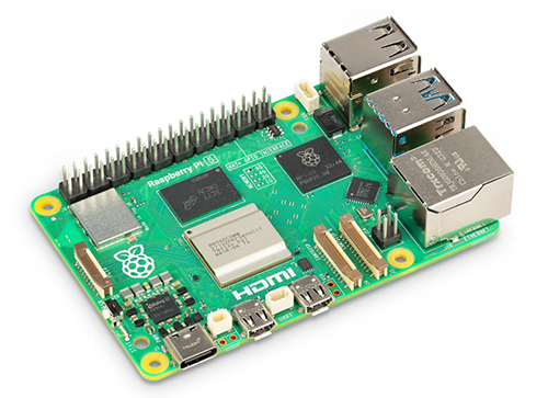
SC1112

Raspberry Pi

$79.61 - $86.40

IN STOCK 10275
Buy

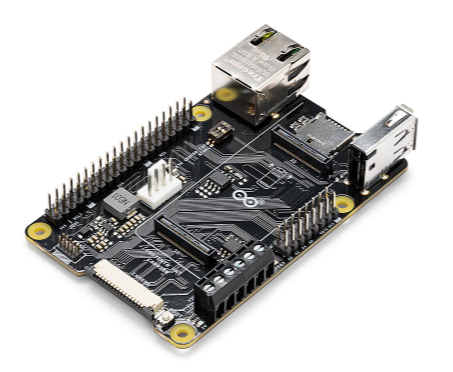
ASX00049

Arduino

* $39.41 - * $44.41

IN STOCK 3132
Buy

AD96685BRZ

Analog Devices Inc.

$1.72 - * $11.79

IN STOCK 4921
Buy

Reference Designs

RD006

Wurth Elektronik

RD006 - 3 W Dual-output isolated auxiliary supply for communication interfaces and measurement systems

CN0583

Analog Devices Inc.

Multistandard Micropower Verified Smoke Detection System-on-Module

Technical Resources

EVALUATION KITS

EVAL-AD7124-8SDZ

Analog Devices Inc.

$71.02 - * $75.98

IN STOCK 808
Buy
View All