ADUM5211BRSZ-RL7
Part Number : ADUM5211BRSZ-RL7
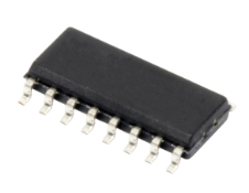
Analog Devices Inc.The ADuM5210 /ADuM5211 / ADuM5212 are dual-channel digitalisolators with isoPower®, an integrated, isolated dc-to-dc converter. Based on the Analog Devices, Inc., iCoupler® technology, the dc-to-dc converter provides regulated, isolated power that is adjustablebetween 3.135 V and 5.25 V. Input supply voltages can range from slightly below the required output to significantly higher. Popularvoltage combinations and their associated power levels are shown in Table 2 in the data sheet.The ADuM5210 / ADuM5211 / ADuM5212 eliminate the need for aseparate, isolated dc-to-dc converter in low power, isolated designs.The iCoupler chip-scale transformer technology is used for isolatedlogic signals and for the magnetic components of the dc-to-dcconverter. The result is a small form factor, total isolationsolution.isoPower uses high frequency switching elements to transfer power through its transformer. Take special care during printed circuit board (PCB) layout to meet emissions standards. See the AN-0971 Application Note for board layout recommendations.APPLICATIONS RS-232 transceivers Power supply start-up bias and gate drives Isolated sensor interfaces Industrial PLCs
ADUM5212BRSZ
Part Number : ADUM5212BRSZ
Analog Devices Inc.The ADuM5210 / ADuM5211 / ADuM5212 are dual-channel digitalisolators with isoPower®, an integrated, isolated dc-to-dc converter. Based on the Analog Devices, Inc., iCoupler® technology, the dc-to-dc converter provides regulated, isolated power that is adjustablebetween 3.135 V and 5.25 V. Input supply voltages can range from slightly below the required output to significantly higher. Popularvoltage combinations and their associated power levels are shown in Table 2 in the data sheet.The ADuM5210 / ADuM5211 / ADuM5212 eliminate the need for aseparate, isolated dc-to-dc converter in low power, isolated designs.The iCoupler chip-scale transformer technology is used for isolatedlogic signals and for the magnetic components of the dc-to-dcconverter. The result is a small form factor, total isolationsolution.isoPower uses high frequency switching elements to transfer power through its transformer. Take special care during printed circuit board (PCB) layout to meet emissions standards. See the AN-0971 Application Note for board layout recommendations.APPLICATIONS RS-232 transceivers Power supply start-up bias and gate drives Isolated sensor interfaces Industrial PLCs
ADUM7223BCCZ-RL7
Part Number : ADUM7223BCCZ-RL7
Analog Devices Inc.The ADuM7223 is a 4A isolated, half-bridge gate driver that employ Analog Devices, Inc.’s iCoupler® technology to provide independent and isolated high-side and low-side outputs. Combining high speed CMOS and monolithic transformer technology, these isolation components provide outstanding performance characteristics superior to alternatives such as the combination of pulse transformers and non-isolated gate drivers. By integrating the isolator and driver in a single package, propagation delay is a maximum of only 60 ns and the propagation skew from channel to channel is a maximum of only 7ns.The ADuM7223 provides two independent isolation channels.The ADuM7223 operates with an input supply ranging from 3.0 V to 5.5 V, providing compatibility with lower voltage systems. The outputs operate in a wide range from 4.5V to 18V with three output voltage versions available. The 5 × 5 mm, LGA package provides 565 V operating voltage from input to output and 700 V from output to output.In comparison to gate drivers employing high voltage level translation methodologies, these gate drivers offer the benefit of true, galvanic isolation between the input and each output. As a result, these gate drivers provide reliable control over the switching characteristics of IGBT/MOSFET configurations over a wide range of positive or negative switching voltages.APPLICATIONS Switching power supplies Isolated IGBT/MOSFET gate drives Industrial inverters
ADV7610BBCZ
Part Number : ADV7610BBCZ
Analog Devices Inc.The ADV7610 is offered in professional (no HDCP) and industrial versions. The operating temperature range is −40°C to +85°C.The ADV7610 is a high quality, single input HDMI-capable receiver. It incorporates an HDMI-capable receiver that supports all mandatory 3D TV defined in HDMI specification. The ADV7610 supports formats up to UXGA 60 Hz at eight bits.It integrates a CEC controller that supports the capability discovery and control (CDC) feature.The ADV7610 has a 4-channel stereo audio output port for the audio data extracted from the HDMI stream. The HDMI receiver has an advanced mute controller that prevents audible extraneous noise in the audio output.The following audio formats are accessible: Four streams from the I2S serializer (eight channels) A stream from the S/PDIF serializer (two uncompressed channels or N compressed channels, for example, AC3) A DST streamThe HDMI port has dedicated 5 V detect and Hot Plug assert pins. The HDMI receiver also includes an integrated equalizer that ensures the robust operation of the interface with long cables.The ADV7610 contains one main component processor (CP) that processes the video signals from the HDMI receiver. It provides features such as contrast, brightness, saturation adjustments, STDI detection block, free run, and synchronization alignment controls.Fabricated in an advanced CMOS process, the ADV7610 is provided in a 6 mm × 6 mm, 76-ball CSP_BGA, RoHS-compliant package and is specified over the −40°C to +85°C temperature range.APPLICATIONS Portable applications Pico projectors Digital video cameras
ADV8005KBCZ-8C
Part Number : ADV8005KBCZ-8C
Analog Devices Inc.The ADV8005 is a multiple input video signal processor that can deinterlace and scale standard definition (SD), enhanced definition (ED), or high definition (HD) video data to ultra HD formats; generate a bitmap on-screen display (OSD); and output the video with OSD overlaid on two High-Definition Multimedia Interface (HDMI®) transmitters and a video encoder.The 60-bit TTL video port can be used to input video to the ADV8005 in a number of ways: using the 48-bit TTL pixel port, using the 24-bit external OSD TTL pixel port, or from a device with an HDMI transmitter such as the ADV7850. The ADV8005 supports many of the formats outlined in the CEA-861-F and VESA specifications, as well as several other widely used timing formats.The ADV8005 features primary and secondary video scalers that enable simultaneous output of multiple different resolutions. The primary video scaler can upscale to 4k × 2k modes. The secondary video scaler can upscale to 1080p or UXGA graphics. 4k × 2k downscaling is performed using the secondary video scaler, leaving the primary video scaler available for other video processing.The ADV8005 primary video scaler can perform high performance, motion adaptive interlaced to progressive conversion on SD and HD content. Additional functionality has also been added to ADV8005 to facilitate upscaling and downscaling to VESA formats with pixel clock frequencies below 300 MHz.Detail enhancement and image enhancing techniques such as random, mosquito, and block noise reduction allow improved final image quality. The frame rate converter of the ADV8005 allows the conversion between common frame rates with support to output two different frame rates simultaneously under certain conditions. The VSP can do aspect ratio conversion, CUE correction, crop output image.The ADV8005 can accept OSD video from an external OSD source on one of its inputs and it can internally generate a high quality, bitmap-based OSD. The internal OSD is highly flexible and allows the system designer to easily incorporate features like scrolling text and animation in various color depths up to 24-bit true color with alpha blending, such as RGB565, ARGB4444 and ARGB8888.Analog Devices, Inc., provides an OSD development tool (Blimp) to assist in the design, debug, and emulation of the OSD prior to integration with the system application. When the design is complete, the OSD development tool automatically generates code to which system application programming interfaces (APIs) can be added before integration with the system application and an OSD design resource, which must be downloaded to an external SPI flash memory.Video can be output from the ADV8005 using one or both of the HDMI transmitters and/or the six-DAC SD/HD video encoder. The six 12-bit NSV® video DACs allow composite (CVBS), S-Video (Y/C), and component (YPrPb) analog outputs in standard, enhanced, and high definition video formats. Oversampling of 216 MHz (SD and ED) and 297 MHz (HD) removes the requirement for external output filtering. Rovi® and non-Rovi variants of the ADV8005 are available.Both of the HDMI transmitters on the ADV8005 support 4k × 2k and all mandatory and many optional 3D video resolutions. Each transmitter features an audio return channel receiver (ARC). The ADV8005 can receive up to eight channels of I2S, S/PDIF, direct stream digital (DSD), and high bit rate (HBR) audio passed from either the serial video Rx or from the externally available audio input pins.The ADV8005 supports the I2C protocol for communication with the system microcontroller. APPLICATIONS High end A/V receivers Upconverting DVD players/recorders Video conferencing and distribution HDMI splitters Video walls 4k HDMI transmitter
ADXRS649BBGZ
Part Number : ADXRS649BBGZ
Analog Devices Inc.The ADXRS64x family of low noise, vibration rejecting yaw rate gyroscopes are drop-in performance upgrades to existing designs using the ADXRS62x family.The ADXRS649 is pin- and package-compatible to the ADXRS62x family and offers the highest rate of rotation sensing available with ±20,000°/sec and fast 3 millisecond (ms) startup for quick power cycling. This measurement range is extendable to ±50,000°/sec with the addition of an external resistor. It is ideally suited for applications where exceptionally wide measurement ranges are needed.The ADXRS649 is a complete angular rate sensor (gyroscope) that uses the Analog Devices, Inc., patented high volume BiMOS surface-micromachining process to make a complete gyro on one chip. An advanced, differential, quad sensor design rejects the influence of linear acceleration, enabling the ADXRS649 to offer rate sensing in harsh environments where shock and vibration are present.The output signal, RATEOUT (B1, A2), is a voltage proportional to the angular rate about the axis normal to the top surface of the package. The output is ratiometric with respect to a provided reference supply. An external capacitor is used to set the band-width. The measurement range is extendable to ±50,000°/sec by adding an external resistor. Low power consumption (3.5 mA) enables very low power consumption, and ultrafast startup (3 ms) allows for quick power cycling of the gyro. At 10 samples per second, a pair of CR2032 coin cells can power the ADXRS649 for three months.A temperature output is provided for compensation techniques. Two digital self-test inputs electromechanically excite the sensor to test proper operation of both the sensor and the signal condi-tioning circuits. The ADXRS649 is available in a 7 mm × 7 mm × 3 mm CBGA chip scale package.Applications Sports equipment Industrial applications Form stabilization High speed tachometry
DC1564A-G
Part Number : DC1564A-G
Analog Devices Inc.The LTC2158-14 is a 2-channel simultaneous sampling 310Msps 14-bit A/D converter designed for digitizing high frequency, wide dynamic range signals. It is perfect for demanding communications applications with AC performance that includes 68.8dB SNR and 88dB spurious free dynamic range (SFDR). The 1.25GHz input bandwidth allows the ADC to undersample high frequencies with good performance. The latency is only five clock cycles.DC specs include ±1.2LSB INL (typ), ±0.35LSB DNL (typ) and no missing codes over temperature. The transition noise is 2.11LSBRMS.The digital outputs are double data rate (DDR) LVDS.The ENC+ and ENC– inputs can be driven differentially with a sine wave, PECL, LVDS, TTL, or CMOS inputs. An optional clock Bits LTC2158-12 12 LTC2158-14 14 Applications Communications Cellular Basestations Software Defined Radios Medical Imaging High Definition Video Testing and Measurement Instruments
DC1620A-R
Part Number : DC1620A-R
Analog Devices Inc.The LTC2142-12/LTC2141-12/LTC2140-12 are 2-channel simultaneous sampling 12-bit A/D converters designed for digitizing high frequency, wide dynamic range signals. They are perfect for demanding communications applications with AC performance that includes 70.8dB SNR and 89dB spurious free dynamic range (SFDR). Ultralow jitter of 0.08psRMS allows undersampling of IF frequencies with excellent noise performance.DC specs include ±0.3LSB INL (typ), ±0.1LSB DNL (typ) and no missing codes over temperature. The transition noise is 0.3LSBRMS.The digital outputs can be either full rate CMOS, double data rate CMOS, or double data rate LVDS. A separate output power supply allows the CMOS output swing to range from 1.2V to 1.8V.The ENC+ and ENC– inputs may be driven differentially or single-ended with a sine wave, PECL, LVDS, TTL, or CMOS inputs. An optional clock duty cycle stabilizer allows high performance at full speed for a wide range of clock duty cycles. Bits LTC2140-12 12 LTC2140-14 14 Applications Communications Cellular Base Stations Software Defined Radios Portable Medical Imaging Multi-Channel Data Acquisition Nondestructive Testing
DC1684A-A
Part Number : DC1684A-A
Analog Devices Inc.The LTC2758 is a dual 18-bit multiplying serial-input, current-output digital-to-analog converter. LTC2758A provides full 18-bit performance (INL and DNL of ±1LSB maximum) over temperature without any adjustments. 18-bit monotonicity is guaranteed in all performance grades. This SoftSpan™ DAC operates from a single 3V to 5V supply and offers six output ranges (up to ±10V) that can be programmed through the 3-wire SPI serial interface or pin-strapped for operation in a single range.Any on-chip register (including DAC output-range settings) can be read for verification in just one instruction cycle; and if you change register content, the altered register will be automatically read back during the next instruction cycle.Voltage-controlled offset and gain adjustments are also provided; and the power-on reset circuit and CLR pin both reset the DAC outputs to 0V regardless of output range.Applications Instrumentation Medical Devices Automatic Test Equipment Process Control and Industrial Automation
DC1759A
Part Number : DC1759A
Analog Devices Inc.The LTM4620A is a complete dual 13A, or single 26A output switching mode DC/DC power supply with wider VOUT range and higher efficiency than the LTM4620. Included in the package are the switching controller, power FETs, inductors and all supporting components. Operating from an input voltage range of 4.5V to 16V, the LTM4620A supports two outputs each with an output voltage range of 0.6V to 5.3V, set by a single external resistor. Its high efficiency design delivers up to 13A continuous current for each output. Only a few input and output capacitors are needed.The device supports frequency synchronization, multiphase operation, Burst Mode® operation and output voltage tracking for supply rail sequencing and has an onboard temperature diode for device temperature monitoring. High switching frequency and a current mode architecture enable a very fast transient response to line and load changes without sacrificing stability.Fault protection features include overvoltage and overcurrent protection. The power module is offered in a proprietary space saving and thermally enhanced 15mm × 15mm × 4.41mm LGA package and 15mm × 15mm × 5.01mm BGA package. The LTM4620A is available with SnPb (BGA) or RoHS compliant terminal finish. Vout Range Efficiency 12Vin, 1.2Vout LTM4620 0.6V-2.5V 83% LTM4620A 0.6V-5.3V 86% Applications Telecom and Networking Equipment Industrial Equipment
DC1805A-C
Part Number : DC1805A-C
Analog Devices Inc.The LTC2377-16 is a low noise, low power, high speed 16-bit successive approximation register (SAR) ADC. Operating from a 2.5V supply, the LTC2377-16 has a ±VREF fully differential input range with VREF ranging from 2.5V to 5.1V. The LTC2377-16 consumes only 6.8mW and achieves ±0.5LSB INL maximum, no missing codes at 16 bits with 97dB SNR.The LTC2377-16 has a high speed SPI-compatible serial interface that supports 1.8V, 2.5V, 3.3V and 5V logic while also featuring a daisy-chain mode. The fast 500ksps throughput with no cycle latency makes the LTC2377-16 ideally suited for a wide variety of high speed applications. An internal oscillator sets the conversion time, easing external timing considerations. The LTC2377-16 automatically powers down between conversions, leading to reduced power dissipation that scales with the sampling rate.The LTC2377-16 features a unique digital gain compression (DGC) function, which eliminates the driver amplifier’s negative supply while preserving the full resolution of the ADC. When enabled, the ADC performs a digital scaling function that maps zero-scale code from 0V to 0.1 • VREF and full-scale code from VREF to 0.9 • VREF. For a typical reference voltage of 5V, the full-scale input range is now 0.5V to 4.5V, which provides adequate headroom for powering the driving amplifier from a single 5.5V supply.Applications Medical Imaging High Speed Data Acquisition Portable or Compact Instrumentation Industrial Process Control Low Power Battery-Operated Instrumentation ATE
DC1813A-C
Part Number : DC1813A-C
Analog Devices Inc.The LTC2367-16 is a low noise, low power, high speed 16-bit successive approximation register (SAR) ADC. Operating from a 2.5V supply, the LTC2367-16 has a 0V to VREF pseudo-differential unipolar input range with VREF ranging from 2.5V to 5.1V. The LTC2367-16 consumes only 6.8mW and achieves ±0.75LSB INL maximum, no missing codes at 16 bits with 94.7dB SNR.The LTC2367-16 has a high speed SPI-compatible serial interface that supports 1.8V, 2.5V, 3.3V and 5V logic while also featuring a daisy-chain mode. The fast 500ksps throughput with no cycle latency makes the LTC2367-16 ideally suited for a wide variety of high speed applications. An internal oscillator sets the conversion time, easing external timing considerations. The LTC2367-16 automatically powers down between conversions, leading to reduced power dissipation that scales with the sampling rate.Applications Medical Imaging High Speed Data Acquisition Portable or Compact Instrumentation Industrial Process Control Low Power Battery-Operated Instrumentation ATE
DC1884A-B
Part Number : DC1884A-B
Analog Devices Inc.The LTM9011-14/LTM9010-14/LTM9009-14 are 8-channel, simultaneous sampling 14-bit A/D converters designed for digitizing high frequency, wide dynamic range signals. AC performance includes 73.1dB SNR and 88dB spurious free dynamic range (SFDR). Low power consumption per channel reduces heat in high channel count applications. Integrated bypass capacitance and flow-through pinout reduces overall board space requirements.DC specs include ±1LSB INL (typ), ±0.3LSB DNL (typ) and no missing codes over temperature. The transition noise is a low 1.2LSBRMS.The digital outputs are serial LVDS to minimize the number of data lines. Each channel outputs two bits at a time (2-lane mode). At lower sampling rates there is a one bit per channel option (1-lane mode).The ENC+ and ENC– inputs may be driven differentially or single-ended with a sine wave, PECL, LVDS, TTL, or CMOS inputs. An internal clock duty cycle stabilizer allows high performance at full speed for a wide range of clock duty cycles.Applications Communications Cellular Base Stations Software Defined Radios Portable Medical Imaging Multichannel Data Acquisition Nondestructive Testing
DC2007A-A
Part Number : DC2007A-A
Analog Devices Inc.The LTM4630 is a dual 18A or single 36A output switching mode step-down DC/DC μModule® (power module) regulator. Included in the package are the switching controllers, power FETs, inductors, and all supporting components. Operating from an input voltage range of 4.5V to 15V, the LTM4630 supports two outputs each with an output voltage range of 0.6V to 1.8V, each set by a single external resistor. Its high efficiency design delivers up to 18A continuous current for each output. Only a few input and output capacitors are needed. The LTM4630 is pin compatible with the LTM4620 and LTM4620A (dual 13A, single 26A) and the LTM4628 (dual 8A, single 16A).The device supports frequency synchronization, multiphase operation, Burst Mode operation and output voltage tracking for supply rail sequencing and has an onboard temperature diode for device temperature monitoring. High switching frequency and a current mode architecture enable a very fast transient response to line and load changes without sacrificing stability.Fault protection features include overvoltage and overcurrent protection. The LTM4630 is offered in 16mm × 16mm × 4.41mm LGA and 16mm × 16mm × 5.01mm BGA packages. The LTM4630 is ROHS compliant. Features Vout LTM4630 0.6V to 1.8V LTM4630-1 0.8% DC and 3% Transient Accuracy 0.6V to 1.8V LTM4630A Higher Light Load Efficiency 0.6V to 5.3V Applications Telecom and Networking Equipment Storage and ATCA Cards Industrial Equipment
DC2007A-C
Part Number : DC2007A-C
Analog Devices Inc.The LTM4630 is a dual 18A or single 36A output switching mode step-down DC/DC μModule® (power module) regulator. Included in the package are the switching controllers, power FETs, inductors, and all supporting components. Operating from an input voltage range of 4.5V to 15V, the LTM4630 supports two outputs each with an output voltage range of 0.6V to 1.8V, each set by a single external resistor. Its high efficiency design delivers up to 18A continuous current for each output. Only a few input and output capacitors are needed. The LTM4630 is pin compatible with the LTM4620 and LTM4620A (dual 13A, single 26A) and the LTM4628 (dual 8A, single 16A).The device supports frequency synchronization, multiphase operation, Burst Mode operation and output voltage tracking for supply rail sequencing and has an onboard temperature diode for device temperature monitoring. High switching frequency and a current mode architecture enable a very fast transient response to line and load changes without sacrificing stability.Fault protection features include overvoltage and overcurrent protection. The LTM4630 is offered in 16mm × 16mm × 4.41mm LGA and 16mm × 16mm × 5.01mm BGA packages. The LTM4630 is ROHS compliant. Features Vout LTM4630 0.6V to 1.8V LTM4630-1 0.8% DC and 3% Transient Accuracy 0.6V to 1.8V LTM4630A Higher Light Load Efficiency 0.6V to 5.3V Applications Telecom and Networking Equipment Storage and ATCA Cards Industrial Equipment
DC2041A
Part Number : DC2041A
Analog Devices Inc.The LTC3255 is a switched-capacitor step-down DC/DC converter that produces a regulated output (2.4V to 12.5V adjustable) from a 4V to 48V input. In applications where the input voltage exceeds twice the output voltage, 2:1 capacitive charge pumping extends output current capability beyond input supply current limits. At no load, Burst Mode® operation cuts VIN quiescent current to 16μA.With its integrated VIN shunt regulator, the LTC3255 excels in 4mA to 20mA current loop applications. The device enables current multiplication; a 4mA input current can power a 7.4mA load continuously. Alternatively, the LTC3255 serves as a higher efficiency replacement for linear regulators and provides a space-saving inductorfree alternative to buck DC/DC converters.The LTC3255 withstands reverse-polarity input supplies and output short-circuits without damage. Safety features including current limit and overtemperature protection further enhance robustness. The LTC3255 is available in thermally enhanced 10-lead MSOP and low profile 3mm × 3mm 10-lead DFN packages.Applications Industrial Control, Factory Automation, Sensors, and SCADA Systems Housekeeping Power Supplies Current-Boosting Voltage Regulators for 4mA to 20mA Current Loops
DC2070A
Part Number : DC2070A
Analog Devices Inc.The LTC5577 active mixer is optimized for RF downconverting applications that require high input signal handling capability and wide bandwidth. The wideband IF output uses external resistors to set the output impedance, allowing the flexibility to match directly into differential IF loads, such as filters and amplifiers. The part is characterized and specified with a 100Ω differential output impedance, although it can be used with output impedances ranging from 50Ω to 400Ω, with higher gain and reduced IIP3 and P1dB at the higher impedance levels. The IF output is usable up to 1.5GHz.In receiver applications, the high input P1dB and IIP3 allow the use of higher gain low noise amplifiers, resulting in higher receiver sensitivity. Integrated transformers on the RF and LO inputs provide single-ended 50Ω interfaces, while minimizing the solution size.Applications Wireless Infrastructure Receivers DPD Observation Receivers CATV Infrastructure
EVAL-AD7176-2SDZ
Part Number : EVAL-AD7176-2SDZ
Analog Devices Inc.The AD7176-2 is a fast settling, highly accurate, high resolution,multiplexed Σ-Δ analog-to-digital converter (ADC) for low bandwidthinput signals. Its inputs can be configured as two fullydifferential or four pseudo differential inputs via the integratedcrosspoint multiplexer. An integrated precision, 2.5 V, low drift(2 ppm/°C), band gap internal reference (with an outputreference buffer) adds functionality and reduces the externalcomponent count.The maximum channel scan data rate is 50 kSPS/channel(settling time of 20 µs), resulting in fully settled data with17 noise free bits. User-selectable output data rates range from5 SPS to 250 kSPS. The resolution increases at lower speeds.The AD7176-2 offers three key digital filters. The fast settlingsinc5 + sinc1 filter maximizes the channel scan rate. The sinc3filter maximizes the resolution for single-channel, low speedapplications. For 50 Hz and 60 Hz environments, the AD7176-2specific filter minimizes the settling times or maximizes therejection of the line frequency. These enhanced filters enablesimultaneous 50 Hz and 60 Hz rejection with a 27 SPS outputdata rate (with a settling time of 36 ms).System offset and gain errors can be corrected on a per channelbasis. This per channel configurability extends to the output datarate used for each channel when using a sinc5 + sinc1 filter. Allswitching of the crosspoint multiplexer is controlled by the ADCand can be configured to automatically control an externalmultiplexer via the GPIO pins.The specified operating temperature range is −40°C to +105°C.The AD7176-2 is housed in a 24-lead TSSOP package.Applications Process control: PLC/DCS modules - Temperature and pressure measurement Medical and scientific multichannel instrumentation Chromatography
EVAL-ADUM1441EBZ
Part Number : EVAL-ADUM1441EBZ
Analog Devices Inc.The ADuM1440/ADuM1441/ADuM1442/ADuM1445/ADuM1446/ADuM1447 are micropower, 4-channel digital isolators based on the Analog Devices, Inc., iCoupler® technology. Combining high speed, complementary metal oxide semiconductor (CMOS) and monolithic air core transformer technologies, these isolation components provide outstanding performance characteristics superior to the alternatives, such as optocoupler devices. As shown in Figure 3 in the data sheet, in standard operating mode, when ENx = 0 (internal refresh enabled), the current per channel is less than 10 μA. When ENx = 1 (internal refresh disabled), the current per channel drops to less than 1 μA.The ADuM1440/ADuM1441/ADuM1442/ADuM1445/ADuM1446/ADuM1447 family of quad 2.5 kV digital isolation devices are packaged in a small 16-lead QSOP and 20-lead SSOP, freeing almost 70% of board space compared to isolators packages in wide body SOIC packages.The devices withstand high isolation voltages and meet regulatory requirements, such as UL and CSA standards. In addition to the space savings, the ADuM1440/ADuM1441/ADuM1442/ADuM1445/ADuM1446/ADuM1447 operate with supplies as low as 2.25 V.Despite the low power consumption, all models of the ADuM1440/ADuM1441/ADuM1442/ADuM1445/ADuM1446/ADuM1447 provide low, pulse width distortion at
HMC996LP4E
Part Number : HMC996LP4E
Analog Devices Inc.The HMC996LP4E is a GaAs PHEMT MMIC analog variable gain amplifier and / or driver amplifier which operates between 5 and 12 GHz. Ideal for microwave radio applications, the amplifier provides up to 18.5 dB of gain, output P1dB of up to +23 dBm, and up to +34 dBm of output IP3 at maximum gain, while requiring only 170 mA from a +5V supply. Gain control voltage pin (Vctrl) is provided to allow variable gain control up to 22 dB. Gain flatness is excellent making the HMC996LP4E ideal for EW, ECM and radar applications. The HMC996LP4E is housed in a RoHS compliant 4 x 4 mm QFN leadless package and is compatible with high volume surface mount manufacturing.Applications Point-to-Point Radio Point-to-Multi-Point Radio EW & ECM Subsystems X-Band Radar Test Equipment & Sensors


