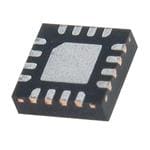
HMC368LP4E
Part Number : HMC368LP4E
Analog Devices Inc.RF Amplifier x2 Active mult SMT, 9 - 16 GHz Fout
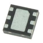
HMC988LP3E
Part Number : HMC988LP3E
Analog Devices Inc.Prescaler Divider 1,2,4,16,32, Variable Delay 4GHz
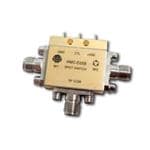
HMC-C058
Part Number : HMC-C058
Analog Devices Inc.RF Switch ICs GaAs MMIC SPDT Non-ReflectSwtch DC-18GHz
ADF4156BCPZ-RL7
Part Number : ADF4156BCPZ-RL7
Analog Devices Inc.The ADF4156 is a 6.2 GHz fractional-N frequency synthesizer that implements local oscillators in the up-conversion and down-conversion sections of wireless receivers and transmitters. It consists of a low noise digital phase frequency detector (PFD), a precision charge pump, and a programmable reference divider. There is a ∑∆ based fractional interpolator to allow programmable fractional-N division. The INT, FRAC, and MOD registers define an overall N divider (N = (INT + (FRAC/MOD))). The RF output phase is programmable for applications that require a particular phase relationship between the output and the reference. The ADF4156 also features cycle slip reduction circuitry, leading to faster lock times without the need for modifications to the loop filter.Control of all on-chip registers is via a simple 3-wire interface. The device operates with a power supply ranging from 2.7 V to 3.3 V and can be powered down when not in use.ApplicationsCATV equipmentBase stations for mobile radio (WiMAX, GSM, PCS, DCS, SuperCell 3G, CDMA, WCDMA)Wireless handsets (GSM, PCS, DCS, CDMA, WCDMA)Wireless LANs, PMRCommunications test equipment
ADF4156BRUZ-RL7
Part Number : ADF4156BRUZ-RL7
Analog Devices Inc.The ADF4156 is a 6.2 GHz fractional-N frequency synthesizer that implements local oscillators in the up-conversion and down-conversion sections of wireless receivers and transmitters. It consists of a low noise digital phase frequency detector (PFD), a precision charge pump, and a programmable reference divider. There is a ∑∆ based fractional interpolator to allow programmable fractional-N division. The INT, FRAC, and MOD registers define an overall N divider (N = (INT + (FRAC/MOD))). The RF output phase is programmable for applications that require a particular phase relationship between the output and the reference. The ADF4156 also features cycle slip reduction circuitry, leading to faster lock times without the need for modifications to the loop filter.Control of all on-chip registers is via a simple 3-wire interface. The device operates with a power supply ranging from 2.7 V to 3.3 V and can be powered down when not in use.ApplicationsCATV equipmentBase stations for mobile radio (WiMAX, GSM, PCS, DCS, SuperCell 3G, CDMA, WCDMA)Wireless handsets (GSM, PCS, DCS, CDMA, WCDMA)Wireless LANs, PMRCommunications test equipment
ADG1234YRUZ
Part Number : ADG1234YRUZ
Analog Devices Inc.The ADG1233 and ADG1234 are monolithic iCMOS® analogswitches comprising three independently selectable single-pole,double throw SPDT switches and four independently selectableSPDT switches, respectively.All channels exhibit break-before-make switching actionpreventing momentary shorting when switching channels. AnEN input on the ADG1233 and ADG1234 enables or disablesthe device. When disabled, all channels are switched off.The iCMOS (industrial-CMOS) modular manufacturing processcombines a high voltage complementary metal-oxide semiconductor(CMOS) and bipolar technologies. It enables thedevelopment of a wide range of high performance analog ICscapable of 33 V operation in a footprint that no other generation ofhigh voltage devices has been able to achieve.Unlike analog ICs using conventional CMOS processes, iCMOScomponents can tolerate high supply voltages while providingincreased performance, dramatically lowered power consumption,and reduced package size.The ultralow capacitance and charge injection of these multiplexersmake them ideal solutions for data acquisition and sample-andholdapplications, where low glitch and fast settling are required.Fast switching speed coupled with high signal bandwidth make thedevices suitable for video signal switching. iCMOS constructionensures ultralow power dissipation, making the devices ideallysuited for portable and battery-powered instruments.Product Highlights 1.5 pF off capacitance (±15 V supply). 0.5 pC charge injection. 3 V logic-compatible digital input, VIH = 2.0 V, VIL = 0.8 V. 16-lead TSSOP, 20-lead TSSOP, and 4 mm × 4 mm LFCSP.Applications Audio and video routing Automatic test equipment Data acquisition systems Battery-powered systems Sample-and-hold systems Communication systems
ADG2128BCPZ-REEL7
Part Number : ADG2128BCPZ-REEL7
Analog Devices Inc.The ADG2128 is an analog cross point switch with an array size of 8 × 12. The switch array is arranged so that there are eight columns by 12 rows, for a total of 96 switch channels. The array is bidirectional, and the rows and columns can be configured as either inputs or outputs. Each of the 96 switches can be addressed and configured through the I2C compatible interface. Standard, full speed, and high speed (3.4 MHz) I2C interfaces are supported. Any simultaneous switch combination is allowed. An additional feature of the ADG2128 is that switches can be updated simultaneously, using the LDSW command. In addition, a RESET option allows all of the switch channels to be reset/off. At power-on, all switches are in the off condition. The device is packaged in a 32-lead, 5 mm × 5 mm LFCSP_VQ.APPLICATIONS AV switching in TV Automotive infotainment AV receivers CCTV Ultrasound applications KVM switching Telecom applications Test equipment/instrumentation PBX systems
ADG417BRZ
Part Number : ADG417BRZ
Analog Devices Inc.The ADG417 is a monolithic CMOS SPST switch. This switch is designed on an enhanced LC2MOS process that provides low power dissipation yet gives high switching speed, low on resistance and low leakage currents.The on resistance profile of the ADG417 is very flat over the full analog input range ensuring excellent linearity and low distortion. The part also exhibits high switching speed and high signal bandwidth. CMOS construction ensures ultralow power dissipation making the parts ideally suited for portable and battery powered instruments.The ADG417 switch, which is turned ON with a logic low on the control input, conducts equally well in both directions when ON and has an input signal range that extends to the supplies. In the OFF condition, signal levels up to the supplies are blocked. The ADG417 exhibits break-before-make switching action for use in multiplexer applications. Inherent in the design is low charge injection for minimum transients when switching the digital input.Applications Precision Test Equipment Precision Instrumentation Battery Powered Systems Sample Hold Systems
ADG508FBRNZ
Part Number : ADG508FBRNZ
Analog Devices Inc.The ADG508F and ADG509F are CMOS analog multiplexers, with the ADG508F comprising eight single channels and the ADG509F comprising four differential channels. These multiplexer provides fault protection. Using a series n-channel, p-channel, n-channel MOSFET structure, both device and signal source protection is provided in the event of an overvoltage or power loss. The multiplexer can withstand continuous overvoltage inputs from -40 V to +55 V. During fault conditions with power supplies off, the multiplexer input (or output) appears as an open circuit and only a few nanoamperes of leakage current will flow. This protects not only the multiplexer and the circuitry driven by the multiplexer, but also protects the sensors or signal sources that drive the multiplexer.The ADG508F switches one of eight inputs to a common output as determined by the 3-bit binary address lines A0, A1 and A2. The ADG509F switches one of four differential inputs to a common differential output as determined by the 2-bit binary address lines A0 and A1. An EN input on each device is used to enable or disable the device. When disabled, all channels are switched OFF.PRODUCT HIGHLIGHTS Fault protection. The ADG508F/ADG509F can withstand continuous voltage inputs from −40 V to +55 V. When a fault occurs due to the power supplies being turned off, all the channels are turned off and only a leakage current of a few nanoamperes flows. On channel saturates while fault exists. Low RON. Fast switching times. Break-before-make switching. Switches are guaranteed break-before-make so that input signals are protected against momentary shorting. Trench isolation eliminates latch-up. A dielectric trench separates the p and n-channel MOSFETs thereby preventing latch-up.APPLICATIONS Existing multiplexer applications (both fault-protected and nonfault-protected) New designs requiring multiplexer functions
ADG608BNZ
Part Number : ADG608BNZ
Analog Devices Inc.The ADG608 is a monolithic CMOS analog multiplexer comprising 8 single channels. The ADG608 switches one of eight inputs to a common output as determined by the 3-bit binary address lines A0, A1 and A2. An EN input on both devices is used to enable or disable the device. When disabled, all channels are switched OFF. The ADG608 is designed on an enhanced LC2 MOS process, which provides low power dissipation yet gives high switching speed and low on resistance. Each channel conducts equally well in both directions when ON and has an input signal range which extends to the supplies. In the OFF condition, signal levels up to the supplies are blocked. All channels exhibit break before make switching action preventing momentary shorting when switching channels. Inherent in the design is low charge injection for minimum transients when switching the digital inputs.
ADG608BRZ
Part Number : ADG608BRZ
Analog Devices Inc.The ADG608 is a monolithic CMOS analog multiplexer comprising 8 single channels. The ADG608 switches one of eight inputs to a common output as determined by the 3-bit binary address lines A0, A1 and A2. An EN input on both devices is used to enable or disable the device. When disabled, all channels are switched OFF. The ADG608 is designed on an enhanced LC2 MOS process, which provides low power dissipation yet gives high switching speed and low on resistance. Each channel conducts equally well in both directions when ON and has an input signal range which extends to the supplies. In the OFF condition, signal levels up to the supplies are blocked. All channels exhibit break before make switching action preventing momentary shorting when switching channels. Inherent in the design is low charge injection for minimum transients when switching the digital inputs.
ADG732BCPZ
Part Number : ADG732BCPZ
Analog Devices Inc.The ADG726/ADG732 are monolithic, complementary metal oxide semiconductor (CMOS) 32-channel and dual 16-channel analog multiplexers. The ADG732 switches one of 32 inputs (S1 to S32) to a common output, D, as determined by the 5-bit binary address lines A0, A1, A2, A3, and A4. The ADG726 switches one of 16 inputs as determined by the 4-bit binary address lines A0, A1, A2, and A3.On-chip latches facilitate microprocessor interfacing. The ADG726 may also be configured for differential operation by tying CSA and CSB together. An EN input is used to enable or disable the devices. When disabled, all channels are switched off.These multiplexers are designed on an enhanced submicron process that provides low power dissipation yet gives high switching speed, very low on resistance, and leakage currents. They operate from a single supply of +1.8 V to +5.5 V and a ±2.5 V dual supply, making them ideally suited to a variety of applications. On resistance is in the region of a few ohms and is closely matched between switches and very flat over the full signal range. These devices can operate equally well as either multiplexers or demultiplexers and have an input signal range that extends to the supplies. In the off condition, signal levels up to the supplies are blocked. All channels exhibit break-before-make switching action, preventing momentary shorting when switching channels.The ADG726/ADG732 are available in a 48-lead LFCSP or a 48-lead TQFP. For functionally equivalent devices with serial interface, see the ADG725/ADG731. PRODUCT HIGHLIGHTS +1.8 V to +5.5 V single- or ±2.5 V dual-supply operation. These devices are specified and guaranteed with +5 V ± 10%, +3 V ± 10% single-supply, and ±2.5 V ± 10% dual-supply rails. An on resistance of 4 Ω. Guaranteed break-before-make switching action. 48-lead LFCSP package or 48-lead TQFP package.APPLICATIONS Optical applications Data acquisition systems Communication systems Relay replacement Audio and video switching Battery-powered systems Medical instrumentation Automatic test equipment (ATE)
ADM2486BRWZ
Part Number : ADM2486BRWZ
Analog Devices Inc.The ADM2486 differential bus transceiver is an integrated, galvanically isolated component designed for bidirectional data communication on multipoint bus transmission lines. It is designed for balanced transmission lines and complies with ANSI EIA/TIA-485-A and ISO 8482: 1987(E).The device employs Analog Devices iCoupler® technology to combine a 3-channel isolator, a three-state differential line driver, and a differential input receiver into a single package. The logic side of the device is powered with either a 5 V or a 3 V supply, and the bus side uses an isolated 5 V supply.The ADM2486 driver has an active-high enable feature. The driver differential outputs and the receiver differential inputs are connected internally to form a differential input/output port that imposes minimal loading on the bus when the driver is disabled or when VDD1 or VDD2 = 0 V. Also provided is an active-high receiver disable feature that causes the receive output to enter a high impedance state.The device has current-limiting and thermal shutdown features to protect against output short circuits and situations where bus contention may cause excessive power dissipation. The part is fully specified over the industrial temperature range and is available in a 16-lead, wide body SOIC package.Applications Isolated RS-485/RS-422 interfaces PROFIBUS networks Industrial field networks Multipoint data transmission systems
ADM2486BRWZ-REEL
Part Number : ADM2486BRWZ-REEL
Analog Devices Inc.The ADM2486 differential bus transceiver is an integrated, galvanically isolated component designed for bidirectional data communication on multipoint bus transmission lines. It is designed for balanced transmission lines and complies with ANSI EIA/TIA-485-A and ISO 8482: 1987(E).The device employs Analog Devices iCoupler® technology to combine a 3-channel isolator, a three-state differential line driver, and a differential input receiver into a single package. The logic side of the device is powered with either a 5 V or a 3 V supply, and the bus side uses an isolated 5 V supply.The ADM2486 driver has an active-high enable feature. The driver differential outputs and the receiver differential inputs are connected internally to form a differential input/output port that imposes minimal loading on the bus when the driver is disabled or when VDD1 or VDD2 = 0 V. Also provided is an active-high receiver disable feature that causes the receive output to enter a high impedance state.The device has current-limiting and thermal shutdown features to protect against output short circuits and situations where bus contention may cause excessive power dissipation. The part is fully specified over the industrial temperature range and is available in a 16-lead, wide body SOIC package.Applications Isolated RS-485/RS-422 interfaces PROFIBUS networks Industrial field networks Multipoint data transmission systems
ADM3072EARZ
Part Number : ADM3072EARZ
Analog Devices Inc.The ADM307xE are 3.3 V, low power data transceivers with ±15 kV ESD protection suitable for full- and half-duplex communication on multipoint bus transmission lines. They are designed for balanced data transmission, and they comply with TIA/EIA standards: RS-485 and RS-422.The devices have a ⅛ unit load receiver input impedance, which allows up to 256 transceivers on a bus. Because only one driver should be enabled at any time, the output of a disabled or powered-down driver is tristated to avoid overloading the bus.The receiver inputs have a true fail-safe feature, which eliminates the need for external bias resistors and ensures a logic high output level when the inputs are open or shorted. This guarantees that the receiver outputs are in a known state before communication begins and when communication ceases.Applications Power/energy metering Industrial control Lighting systems Telecommunications Security systems Instrumentation
ADM3202ARNZ
Part Number : ADM3202ARNZ
Analog Devices Inc.The ADM3202 / ADM3222 / ADM1385 are high speed, 2-channel RS232/V.28 interface devices which operate from a single +3.3 V power supply. Low power consumption and a shutdown facility (ADM3222/ADM1385) makes them ideal for battery powered portable instruments.The ADM3202 / ADM3222 / ADM1385 conform to the EIA-232E and CCITT V.28 specifications and operate at data rates up to 230 kbps. Four external 0.1 µF charge pump capacitors are used for the voltage doubler/inverter permitting operation from a single +3.3 V supply.The ADM3222 / ADM1385 contain additional enable and shutdown circuitry. The EN input may be used to three-state the receiver outputs. The SD input is used to power down the charge pump and transmitter outputs reducing the quiescent current to less than 1 µA. The receivers remain enabled during shutdown unless disabled using EN.The ADM3202 is available in a 16-lead DIP, narrow and wide SO as well as a space saving TSSOP package. The ADM3222 is available in 18 lead DIP , SO and in 20 lead SSOP and TSSOP. The ADM1385 is available in a 20 lead SSOP package and is pin compatible with the LTC1385 CG.APPLICATIONS General-purpose RS-232 data link Portable instruments Printers, palmtop computers, PDAs
ADM3310EARUZ
Part Number : ADM3310EARUZ
Analog Devices Inc.The ADM3310E is a three-driver/five-receiver serial port transceiver, which meets EIA-232 standards while operating from a single power supply as low as +2.7V. It is similar to the ADM3311E but with two of the Receivers remain Active during Shutdown. It features an on-board, charge pump dc-to-dc converter, which eliminates the need for dual power supplies.This dc-to-dc converter also contains a voltage tripler and voltage inverter for internally generating positive and negative supplies from the power supply. It operates in Green Idle Mode, where the charge pump oscillator is gated on and off to maintain output voltage to +/-6 V, regardless of the load conditions. Another key feature is its ESD protection: up to +/−15kV on all I/O lines. The ADM3310E is available in a 28-pin TSSOP package as well as a space-saving 5×5mm 32-pin LFCSP package.APPLICATIONS Mobile phone handsets/data cables Laptop and notebook computers Printers Peripherals Modems PDAs/Hand-Held Devices/Palmtop Computers
ADM560JRSZ
Part Number : ADM560JRSZ
Analog Devices Inc.The ADM560 / ADM561 are four driver/five receiver interface devices designed to meet the EIA-232 standard while operating with a single +3.3 V power supply. The devices feature an on-board dc-to-dc converter, eliminating the need for dual ±5 V power supplies. This dc-dc converter contains a voltage doubler and voltage inverter which internally generates ±6.6 V from the input +3.3 V power supply.The ADM560 and ADM561 consume only 5 mW making them ideally suited for battery and other power-sensitive applications. A shutdown facility is also provided which reduces the power to 0.66 µW.The ADM560 contains active low shutdown and active high receiver enable signals. In shutdown mode, two receivers remain active thereby allowing monitoring of peripheral devices. This feature allows the device to be shut down until a peripheral device begins communication. The active receivers can alert the processor which can then take the ADM560 out of the shutdown mode.The ADM561 features active high shutdown and an active low receiver enable. In this device all receivers are disabled in shutdown.The ADM560 / ADM561 is fabricated using CMOS technology for minimal power consumption. It features a high level of over-voltage protection and latch-up immunity. The receiver inputs can withstand up to ±25 V levels. The transmitter inputs can be driven from either 3V or 5V logic levels. This allows operation in mixed 3 V/5 V power supply systems.The ADM560 / ADM561 is packaged in a 28-pin SO and a 28-pin SSOP package.
