LTC2634HMSE-LMI10#PBF
Part Number : LTC2634HMSE-LMI10#PBF
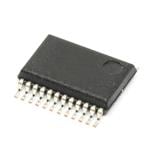
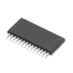
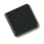
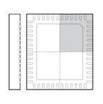
Analog Devices Inc.Quad 12-/10-/8-Bit Rail-to-Rail DACs with 10ppm/C Reference Features: AEC-Q100 Qualified for Automotive Applications Integrated Precision Reference 2.5V Full-Scale 10ppm/°C (LTC2634-L) 4.096V Full-Scale 10ppm/°C (LTC2634-H) Maximum INL Error: ±2.5 LSB (LTC2634-12) Low Noise: 0.75mVP-P 0.1Hz to 200KHzGuaranteed Monotonic over −40°C to 125°C Temperature RangeSelectable Internal or External Reference2.7V to 5.5V Supply Range (LTC2634-L)Ultralow Crosstalk Between DACs (2.4nV•s)Low Power: 0.6mA at 3VPower-On Reset to Zero-Scale/Mid-ScaleDouble Buffered Data LatchesTiny 16-Lead 3mm × 3mm QFN and 10-Lead MSOP Packages
LTC2634HMSE-LMI10#TRPBF
Part Number : LTC2634HMSE-LMI10#TRPBF
Analog Devices Inc.Quad 12-/10-/8-Bit Rail-to-Rail DACs with 10ppm/C Reference Features: AEC-Q100 Qualified for Automotive Applications Integrated Precision Reference 2.5V Full-Scale 10ppm/°C (LTC2634-L) 4.096V Full-Scale 10ppm/°C (LTC2634-H) Maximum INL Error: ±2.5 LSB (LTC2634-12) Low Noise: 0.75mVP-P 0.1Hz to 200KHzGuaranteed Monotonic over −40°C to 125°C Temperature RangeSelectable Internal or External Reference2.7V to 5.5V Supply Range (LTC2634-L)Ultralow Crosstalk Between DACs (2.4nV•s)Low Power: 0.6mA at 3VPower-On Reset to Zero-Scale/Mid-ScaleDouble Buffered Data LatchesTiny 16-Lead 3mm × 3mm QFN and 10-Lead MSOP Packages
LTC2634HMSE-LMX10#PBF
Part Number : LTC2634HMSE-LMX10#PBF
Analog Devices Inc.Quad 12-/10-/8-Bit Rail-to-Rail DACs with 10ppm/C Reference Features: AEC-Q100 Qualified for Automotive Applications Integrated Precision Reference 2.5V Full-Scale 10ppm/°C (LTC2634-L) 4.096V Full-Scale 10ppm/°C (LTC2634-H) Maximum INL Error: ±2.5 LSB (LTC2634-12) Low Noise: 0.75mVP-P 0.1Hz to 200KHzGuaranteed Monotonic over −40°C to 125°C Temperature RangeSelectable Internal or External Reference2.7V to 5.5V Supply Range (LTC2634-L)Ultralow Crosstalk Between DACs (2.4nV•s)Low Power: 0.6mA at 3VPower-On Reset to Zero-Scale/Mid-ScaleDouble Buffered Data LatchesTiny 16-Lead 3mm × 3mm QFN and 10-Lead MSOP Packages
LTC2634HMSE-LMX8#PBF
Part Number : LTC2634HMSE-LMX8#PBF
Analog Devices Inc.Quad 12-/10-/8-Bit Rail-to-Rail DACs with 10ppm/C Reference Features: AEC-Q100 Qualified for Automotive Applications Integrated Precision Reference 2.5V Full-Scale 10ppm/°C (LTC2634-L) 4.096V Full-Scale 10ppm/°C (LTC2634-H) Maximum INL Error: ±2.5 LSB (LTC2634-12) Low Noise: 0.75mVP-P 0.1Hz to 200KHzGuaranteed Monotonic over −40°C to 125°C Temperature RangeSelectable Internal or External Reference2.7V to 5.5V Supply Range (LTC2634-L)Ultralow Crosstalk Between DACs (2.4nV•s)Low Power: 0.6mA at 3VPower-On Reset to Zero-Scale/Mid-ScaleDouble Buffered Data LatchesTiny 16-Lead 3mm × 3mm QFN and 10-Lead MSOP Packages
LTC2634HMSE-LZ12#TRPBF
Part Number : LTC2634HMSE-LZ12#TRPBF
Analog Devices Inc.Quad 12-/10-/8-Bit Rail-to-Rail DACs with 10ppm/C Reference Features: AEC-Q100 Qualified for Automotive Applications Integrated Precision Reference 2.5V Full-Scale 10ppm/°C (LTC2634-L) 4.096V Full-Scale 10ppm/°C (LTC2634-H) Maximum INL Error: ±2.5 LSB (LTC2634-12) Low Noise: 0.75mVP-P 0.1Hz to 200KHzGuaranteed Monotonic over −40°C to 125°C Temperature RangeSelectable Internal or External Reference2.7V to 5.5V Supply Range (LTC2634-L)Ultralow Crosstalk Between DACs (2.4nV•s)Low Power: 0.6mA at 3VPower-On Reset to Zero-Scale/Mid-ScaleDouble Buffered Data LatchesTiny 16-Lead 3mm × 3mm QFN and 10-Lead MSOP Packages