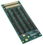
ADZS-BRKOUT-EX3
Part Number : ADZS-BRKOUT-EX3
Analog Devices Inc.ANALOG DEVELOPMENT KIT ACCESSORIES;


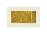
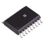
TMC2202-WA-T
Part Number : TMC2202-WA-T
Analog Devices Inc.MOTOR DRIVER, STEPPER, 1 O/P, QFN-32; Motor Type:Stepper; No. of Outputs:1Outputs; Output Current:1.2A; Output Voltage:-; Driver Case Style:QFN; No. of Pins:32Pins; Supply Voltage Min:5.5V; Supply Voltage Max:36V; Operating RoHS Compliant: Yes