MAXQ7667AACM+
Part Number : MAXQ7667AACM+
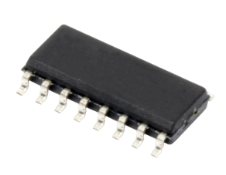
Analog Devices Inc.The MAXQ7667 smart system-on-a-chip (SoC) provides a time-of-flight ultrasonic distance-measuring solution. The device is optimized for applications involving large distance measurement with weak input signals or multiple target identification. The MAXQ7667 features high signal-to-noise ratio achieved by combining flexible electronics with the intelligence necessary to optimize each function as environmental and target conditions change.An integrated burst signal generator and echo reception components process ultrasonic signals between 25kHz and 100kHz. Echo reception components include a programmable gain low-noise amplifier (LNA), a 16-bit sigma-delta ADC to digitize the received echo signals, and digital signal processing (DSP). DSP limits noise with a bandpass filter, and creates an echo envelope through demodulation and lowpass filtering. Input referred noise is a low 0.7µVRMS. A programmable phase-locked loop (PLL) frequency synthesizer supplies the reference frequency for the burst generator and the clock for the echo receiver's digital filter. An embedded 16-bit MAXQ20 microcontroller (µC) controls all the preceding functions.The µC optimizes the burst frequency and reception frequency for each transmission at any temperature. The MAXQ7667 achieves smart sensing by monitoring the echo signals and then actively changing the transmitted and received parameters to obtain optimum results. Digital filtering and burst synthesis do not require CPU intervention. This leaves all the CPU power available for echo optimization, communication, diagnostics, and additional signal processing.The MAXQ7667 operates with three different power supply voltages: +5V, +3.3V, and +2.5V. Two internal linear regulators allow operation from a single +5V supply when three external power supplies are not available. Alternatively, the MAXQ7667 can control an external pass transistor to allow operation from a single supply voltage of +8V to +65V or more, depending on the external component tolerance. The device is available in a 48-pin LQFP package and is specified to operate from -40°C to +125°C. Note: Designers must have the following documents to fully use all the features of this device. This data sheet contains pin descriptions, feature overviews, and electrical specifications. Errata sheets contain deviations from published specifications. The user's guides offer detailed information about device features and operation. MAXQ7667 IC data sheet MAXQ7667 revision-specific errata sheet (Click here for availability) MAXQ7667 User's GuideApplicationsAutomationAutomotive ParkingHandheld DevicesIndustrial ProcessingVehicle Security
MAXQ7667AACM/V+
Part Number : MAXQ7667AACM/V+
Analog Devices Inc.The MAXQ7667 smart system-on-a-chip (SoC) provides a time-of-flight ultrasonic distance-measuring solution. The device is optimized for applications involving large distance measurement with weak input signals or multiple target identification. The MAXQ7667 features high signal-to-noise ratio achieved by combining flexible electronics with the intelligence necessary to optimize each function as environmental and target conditions change.An integrated burst signal generator and echo reception components process ultrasonic signals between 25kHz and 100kHz. Echo reception components include a programmable gain low-noise amplifier (LNA), a 16-bit sigma-delta ADC to digitize the received echo signals, and digital signal processing (DSP). DSP limits noise with a bandpass filter, and creates an echo envelope through demodulation and lowpass filtering. Input referred noise is a low 0.7µVRMS. A programmable phase-locked loop (PLL) frequency synthesizer supplies the reference frequency for the burst generator and the clock for the echo receiver's digital filter. An embedded 16-bit MAXQ20 microcontroller (µC) controls all the preceding functions.The µC optimizes the burst frequency and reception frequency for each transmission at any temperature. The MAXQ7667 achieves smart sensing by monitoring the echo signals and then actively changing the transmitted and received parameters to obtain optimum results. Digital filtering and burst synthesis do not require CPU intervention. This leaves all the CPU power available for echo optimization, communication, diagnostics, and additional signal processing.The MAXQ7667 operates with three different power supply voltages: +5V, +3.3V, and +2.5V. Two internal linear regulators allow operation from a single +5V supply when three external power supplies are not available. Alternatively, the MAXQ7667 can control an external pass transistor to allow operation from a single supply voltage of +8V to +65V or more, depending on the external component tolerance. The device is available in a 48-pin LQFP package and is specified to operate from -40°C to +125°C. Note: Designers must have the following documents to fully use all the features of this device. This data sheet contains pin descriptions, feature overviews, and electrical specifications. Errata sheets contain deviations from published specifications. The user's guides offer detailed information about device features and operation. MAXQ7667 IC data sheet MAXQ7667 revision-specific errata sheet (Click here for availability) MAXQ7667 User's GuideApplicationsAutomationAutomotive ParkingHandheld DevicesIndustrial ProcessingVehicle Security
MAXQ7667AACM/V+T
Part Number : MAXQ7667AACM/V+T
Analog Devices Inc.The MAXQ7667 smart system-on-a-chip (SoC) provides a time-of-flight ultrasonic distance-measuring solution. The device is optimized for applications involving large distance measurement with weak input signals or multiple target identification. The MAXQ7667 features high signal-to-noise ratio achieved by combining flexible electronics with the intelligence necessary to optimize each function as environmental and target conditions change.An integrated burst signal generator and echo reception components process ultrasonic signals between 25kHz and 100kHz. Echo reception components include a programmable gain low-noise amplifier (LNA), a 16-bit sigma-delta ADC to digitize the received echo signals, and digital signal processing (DSP). DSP limits noise with a bandpass filter, and creates an echo envelope through demodulation and lowpass filtering. Input referred noise is a low 0.7µVRMS. A programmable phase-locked loop (PLL) frequency synthesizer supplies the reference frequency for the burst generator and the clock for the echo receiver's digital filter. An embedded 16-bit MAXQ20 microcontroller (µC) controls all the preceding functions.The µC optimizes the burst frequency and reception frequency for each transmission at any temperature. The MAXQ7667 achieves smart sensing by monitoring the echo signals and then actively changing the transmitted and received parameters to obtain optimum results. Digital filtering and burst synthesis do not require CPU intervention. This leaves all the CPU power available for echo optimization, communication, diagnostics, and additional signal processing.The MAXQ7667 operates with three different power supply voltages: +5V, +3.3V, and +2.5V. Two internal linear regulators allow operation from a single +5V supply when three external power supplies are not available. Alternatively, the MAXQ7667 can control an external pass transistor to allow operation from a single supply voltage of +8V to +65V or more, depending on the external component tolerance. The device is available in a 48-pin LQFP package and is specified to operate from -40°C to +125°C. Note: Designers must have the following documents to fully use all the features of this device. This data sheet contains pin descriptions, feature overviews, and electrical specifications. Errata sheets contain deviations from published specifications. The user's guides offer detailed information about device features and operation. MAXQ7667 IC data sheet MAXQ7667 revision-specific errata sheet (Click here for availability) MAXQ7667 User's GuideApplicationsAutomationAutomotive ParkingHandheld DevicesIndustrial ProcessingVehicle Security
LTC2216CUP#PBF
Part Number : LTC2216CUP#PBF
Analog Devices Inc.The LTC2216/LTC2215 are 80Msps/65Msps sampling 16- bit A/D converters designed for digitizing high frequency, wide dynamic range signals with input frequencies up to 400MHz. The input range of the ADC is fixed at 2.75VP-P.The LTC2216/LTC2215 are perfect for demanding communications applications, with AC performance that includes 81.5dBFS noise floor and 100dB spurious free dynamic range (SFDR). Ultra low jitter of 85fsRMS allows undersampling of high input frequencies while maintaining excellent noise performance. Maximum DC specs include ±3.5LSB INL, ±1LSB DNL (no missing codes). The digital output can be either differential LVDS or single-ended CMOS. There are two format options for the CMOS outputs: a single bus running at the full data rate or demultiplexed buses running at half data rate. A separate output power supply allows the CMOS output swing to range from 0.5V to 3.6V. The ENC+ and ENC– inputs may be driven differentially or single-ended with a sine wave, PECL, LVDS, TTL or CMOS inputs. An optional clock duty cycle stabilizer allows high performance at full speed with a wide range of clock duty cycles.Applications Telecommunications Receivers Cellular Base Stations Spectrum Analysis Imaging Systems ATE
LTC2636CMS-LZ8#PBF
Part Number : LTC2636CMS-LZ8#PBF
Analog Devices Inc.The LTC2636 is a family of octal 12-, 10-, and 8-bit voltage-output DACs with an integrated, high-accuracy, low-drift 10ppm/°C reference in 14-lead DFN and 16-lead MSOP packages. It has a rail-to-rail output buffer and is guaranteed monotonic. The LTC2636-L has a full-scale output of 2.5V, and operates from a single 2.7V to 5.5V supply. The LTC2636-H has a full-scale output of 4.096V, and operates from a 4.5V to 5.5V supply. Each DAC can also operate with an external reference, which sets the DAC full-scale output to the external reference voltage.These DACs communicate via an SPI/MICROWIRE-compatible 3-wire serial interface which operates at clock rates up to 50MHz. Hardware clear (CLR) and asynchronous DAC update (LDAC) pins are available in the MSOP package. The LTC2636 incorporates a power-on reset circuit. Options are available for reset to zero-scale or reset to mid-scale in internal reference mode, or reset to mid-scale in external reference mode after power-up.Applications Mobile Communications Process Control and Industrial Automation Automatic Test Equipment Portable Equipment Automotive Optical Networking
LTC2636HMS-LMI12#PBF
Part Number : LTC2636HMS-LMI12#PBF
Analog Devices Inc.The LTC2636 is a family of octal 12-, 10-, and 8-bit voltage-output DACs with an integrated, high-accuracy, low-drift 10ppm/°C reference in 14-lead DFN and 16-lead MSOP packages. It has a rail-to-rail output buffer and is guaranteed monotonic. The LTC2636-L has a full-scale output of 2.5V, and operates from a single 2.7V to 5.5V supply. The LTC2636-H has a full-scale output of 4.096V, and operates from a 4.5V to 5.5V supply. Each DAC can also operate with an external reference, which sets the DAC full-scale output to the external reference voltage.These DACs communicate via an SPI/MICROWIRE-compatible 3-wire serial interface which operates at clock rates up to 50MHz. Hardware clear (CLR) and asynchronous DAC update (LDAC) pins are available in the MSOP package. The LTC2636 incorporates a power-on reset circuit. Options are available for reset to zero-scale or reset to mid-scale in internal reference mode, or reset to mid-scale in external reference mode after power-up.Applications Mobile Communications Process Control and Industrial Automation Automatic Test Equipment Portable Equipment Automotive Optical Networking
LTC2636HMS-LZ10#PBF
Part Number : LTC2636HMS-LZ10#PBF
Analog Devices Inc.The LTC2636 is a family of octal 12-, 10-, and 8-bit voltage-output DACs with an integrated, high-accuracy, low-drift 10ppm/°C reference in 14-lead DFN and 16-lead MSOP packages. It has a rail-to-rail output buffer and is guaranteed monotonic. The LTC2636-L has a full-scale output of 2.5V, and operates from a single 2.7V to 5.5V supply. The LTC2636-H has a full-scale output of 4.096V, and operates from a 4.5V to 5.5V supply. Each DAC can also operate with an external reference, which sets the DAC full-scale output to the external reference voltage.These DACs communicate via an SPI/MICROWIRE-compatible 3-wire serial interface which operates at clock rates up to 50MHz. Hardware clear (CLR) and asynchronous DAC update (LDAC) pins are available in the MSOP package. The LTC2636 incorporates a power-on reset circuit. Options are available for reset to zero-scale or reset to mid-scale in internal reference mode, or reset to mid-scale in external reference mode after power-up.Applications Mobile Communications Process Control and Industrial Automation Automatic Test Equipment Portable Equipment Automotive Optical Networking
LTC2636IDE-HMI10#PBF
Part Number : LTC2636IDE-HMI10#PBF
Analog Devices Inc.The LTC2636 is a family of octal 12-, 10-, and 8-bit voltage-output DACs with an integrated, high-accuracy, low-drift 10ppm/°C reference in 14-lead DFN and 16-lead MSOP packages. It has a rail-to-rail output buffer and is guaranteed monotonic. The LTC2636-L has a full-scale output of 2.5V, and operates from a single 2.7V to 5.5V supply. The LTC2636-H has a full-scale output of 4.096V, and operates from a 4.5V to 5.5V supply. Each DAC can also operate with an external reference, which sets the DAC full-scale output to the external reference voltage.These DACs communicate via an SPI/MICROWIRE-compatible 3-wire serial interface which operates at clock rates up to 50MHz. Hardware clear (CLR) and asynchronous DAC update (LDAC) pins are available in the MSOP package. The LTC2636 incorporates a power-on reset circuit. Options are available for reset to zero-scale or reset to mid-scale in internal reference mode, or reset to mid-scale in external reference mode after power-up.Applications Mobile Communications Process Control and Industrial Automation Automatic Test Equipment Portable Equipment Automotive Optical Networking
LTC2636IDE-HMI12#PBF
Part Number : LTC2636IDE-HMI12#PBF
Analog Devices Inc.The LTC2636 is a family of octal 12-, 10-, and 8-bit voltage-output DACs with an integrated, high-accuracy, low-drift 10ppm/°C reference in 14-lead DFN and 16-lead MSOP packages. It has a rail-to-rail output buffer and is guaranteed monotonic. The LTC2636-L has a full-scale output of 2.5V, and operates from a single 2.7V to 5.5V supply. The LTC2636-H has a full-scale output of 4.096V, and operates from a 4.5V to 5.5V supply. Each DAC can also operate with an external reference, which sets the DAC full-scale output to the external reference voltage.These DACs communicate via an SPI/MICROWIRE-compatible 3-wire serial interface which operates at clock rates up to 50MHz. Hardware clear (CLR) and asynchronous DAC update (LDAC) pins are available in the MSOP package. The LTC2636 incorporates a power-on reset circuit. Options are available for reset to zero-scale or reset to mid-scale in internal reference mode, or reset to mid-scale in external reference mode after power-up.Applications Mobile Communications Process Control and Industrial Automation Automatic Test Equipment Portable Equipment Automotive Optical Networking
LTC2636IDE-HMX8#PBF
Part Number : LTC2636IDE-HMX8#PBF
Analog Devices Inc.The LTC2636 is a family of octal 12-, 10-, and 8-bit voltage-output DACs with an integrated, high-accuracy, low-drift 10ppm/°C reference in 14-lead DFN and 16-lead MSOP packages. It has a rail-to-rail output buffer and is guaranteed monotonic. The LTC2636-L has a full-scale output of 2.5V, and operates from a single 2.7V to 5.5V supply. The LTC2636-H has a full-scale output of 4.096V, and operates from a 4.5V to 5.5V supply. Each DAC can also operate with an external reference, which sets the DAC full-scale output to the external reference voltage.These DACs communicate via an SPI/MICROWIRE-compatible 3-wire serial interface which operates at clock rates up to 50MHz. Hardware clear (CLR) and asynchronous DAC update (LDAC) pins are available in the MSOP package. The LTC2636 incorporates a power-on reset circuit. Options are available for reset to zero-scale or reset to mid-scale in internal reference mode, or reset to mid-scale in external reference mode after power-up.Applications Mobile Communications Process Control and Industrial Automation Automatic Test Equipment Portable Equipment Automotive Optical Networking
LTC2636IDE-HMX8#TRPBF
Part Number : LTC2636IDE-HMX8#TRPBF
Analog Devices Inc.The LTC2636 is a family of octal 12-, 10-, and 8-bit voltage-output DACs with an integrated, high-accuracy, low-drift 10ppm/°C reference in 14-lead DFN and 16-lead MSOP packages. It has a rail-to-rail output buffer and is guaranteed monotonic. The LTC2636-L has a full-scale output of 2.5V, and operates from a single 2.7V to 5.5V supply. The LTC2636-H has a full-scale output of 4.096V, and operates from a 4.5V to 5.5V supply. Each DAC can also operate with an external reference, which sets the DAC full-scale output to the external reference voltage.These DACs communicate via an SPI/MICROWIRE-compatible 3-wire serial interface which operates at clock rates up to 50MHz. Hardware clear (CLR) and asynchronous DAC update (LDAC) pins are available in the MSOP package. The LTC2636 incorporates a power-on reset circuit. Options are available for reset to zero-scale or reset to mid-scale in internal reference mode, or reset to mid-scale in external reference mode after power-up.Applications Mobile Communications Process Control and Industrial Automation Automatic Test Equipment Portable Equipment Automotive Optical Networking
LTC2636IDE-LMX12#TRPBF
Part Number : LTC2636IDE-LMX12#TRPBF
Analog Devices Inc.The LTC2636 is a family of octal 12-, 10-, and 8-bit voltage-output DACs with an integrated, high-accuracy, low-drift 10ppm/°C reference in 14-lead DFN and 16-lead MSOP packages. It has a rail-to-rail output buffer and is guaranteed monotonic. The LTC2636-L has a full-scale output of 2.5V, and operates from a single 2.7V to 5.5V supply. The LTC2636-H has a full-scale output of 4.096V, and operates from a 4.5V to 5.5V supply. Each DAC can also operate with an external reference, which sets the DAC full-scale output to the external reference voltage.These DACs communicate via an SPI/MICROWIRE-compatible 3-wire serial interface which operates at clock rates up to 50MHz. Hardware clear (CLR) and asynchronous DAC update (LDAC) pins are available in the MSOP package. The LTC2636 incorporates a power-on reset circuit. Options are available for reset to zero-scale or reset to mid-scale in internal reference mode, or reset to mid-scale in external reference mode after power-up.Applications Mobile Communications Process Control and Industrial Automation Automatic Test Equipment Portable Equipment Automotive Optical Networking
LTC2636IDE-LZ8#PBF
Part Number : LTC2636IDE-LZ8#PBF
Analog Devices Inc.The LTC2636 is a family of octal 12-, 10-, and 8-bit voltage-output DACs with an integrated, high-accuracy, low-drift 10ppm/°C reference in 14-lead DFN and 16-lead MSOP packages. It has a rail-to-rail output buffer and is guaranteed monotonic. The LTC2636-L has a full-scale output of 2.5V, and operates from a single 2.7V to 5.5V supply. The LTC2636-H has a full-scale output of 4.096V, and operates from a 4.5V to 5.5V supply. Each DAC can also operate with an external reference, which sets the DAC full-scale output to the external reference voltage.These DACs communicate via an SPI/MICROWIRE-compatible 3-wire serial interface which operates at clock rates up to 50MHz. Hardware clear (CLR) and asynchronous DAC update (LDAC) pins are available in the MSOP package. The LTC2636 incorporates a power-on reset circuit. Options are available for reset to zero-scale or reset to mid-scale in internal reference mode, or reset to mid-scale in external reference mode after power-up.Applications Mobile Communications Process Control and Industrial Automation Automatic Test Equipment Portable Equipment Automotive Optical Networking
LTC2636IMS-HMI10#TRPBF
Part Number : LTC2636IMS-HMI10#TRPBF
Analog Devices Inc.The LTC2636 is a family of octal 12-, 10-, and 8-bit voltage-output DACs with an integrated, high-accuracy, low-drift 10ppm/°C reference in 14-lead DFN and 16-lead MSOP packages. It has a rail-to-rail output buffer and is guaranteed monotonic. The LTC2636-L has a full-scale output of 2.5V, and operates from a single 2.7V to 5.5V supply. The LTC2636-H has a full-scale output of 4.096V, and operates from a 4.5V to 5.5V supply. Each DAC can also operate with an external reference, which sets the DAC full-scale output to the external reference voltage.These DACs communicate via an SPI/MICROWIRE-compatible 3-wire serial interface which operates at clock rates up to 50MHz. Hardware clear (CLR) and asynchronous DAC update (LDAC) pins are available in the MSOP package. The LTC2636 incorporates a power-on reset circuit. Options are available for reset to zero-scale or reset to mid-scale in internal reference mode, or reset to mid-scale in external reference mode after power-up.Applications Mobile Communications Process Control and Industrial Automation Automatic Test Equipment Portable Equipment Automotive Optical Networking
LTC2636IMS-HMX12#TRPBF
Part Number : LTC2636IMS-HMX12#TRPBF
Analog Devices Inc.The LTC2636 is a family of octal 12-, 10-, and 8-bit voltage-output DACs with an integrated, high-accuracy, low-drift 10ppm/°C reference in 14-lead DFN and 16-lead MSOP packages. It has a rail-to-rail output buffer and is guaranteed monotonic. The LTC2636-L has a full-scale output of 2.5V, and operates from a single 2.7V to 5.5V supply. The LTC2636-H has a full-scale output of 4.096V, and operates from a 4.5V to 5.5V supply. Each DAC can also operate with an external reference, which sets the DAC full-scale output to the external reference voltage.These DACs communicate via an SPI/MICROWIRE-compatible 3-wire serial interface which operates at clock rates up to 50MHz. Hardware clear (CLR) and asynchronous DAC update (LDAC) pins are available in the MSOP package. The LTC2636 incorporates a power-on reset circuit. Options are available for reset to zero-scale or reset to mid-scale in internal reference mode, or reset to mid-scale in external reference mode after power-up.Applications Mobile Communications Process Control and Industrial Automation Automatic Test Equipment Portable Equipment Automotive Optical Networking
LTC2636IMS-LMI10#PBF
Part Number : LTC2636IMS-LMI10#PBF
Analog Devices Inc.The LTC2636 is a family of octal 12-, 10-, and 8-bit voltage-output DACs with an integrated, high-accuracy, low-drift 10ppm/°C reference in 14-lead DFN and 16-lead MSOP packages. It has a rail-to-rail output buffer and is guaranteed monotonic. The LTC2636-L has a full-scale output of 2.5V, and operates from a single 2.7V to 5.5V supply. The LTC2636-H has a full-scale output of 4.096V, and operates from a 4.5V to 5.5V supply. Each DAC can also operate with an external reference, which sets the DAC full-scale output to the external reference voltage.These DACs communicate via an SPI/MICROWIRE-compatible 3-wire serial interface which operates at clock rates up to 50MHz. Hardware clear (CLR) and asynchronous DAC update (LDAC) pins are available in the MSOP package. The LTC2636 incorporates a power-on reset circuit. Options are available for reset to zero-scale or reset to mid-scale in internal reference mode, or reset to mid-scale in external reference mode after power-up.Applications Mobile Communications Process Control and Industrial Automation Automatic Test Equipment Portable Equipment Automotive Optical Networking
LTC4358CDE#TRPBF
Part Number : LTC4358CDE#TRPBF
Analog Devices Inc.The LTC4358 is a 5A ideal diode that uses an internal 20mΩ N-channel MOSFET to replace a Schottky diode when used in diode-OR and high current diode applications. The LTC4358 reduces power consumption, heat dissipation, and PC board area. The LTC4358 easily ORs power supplies together to increase total system reliability. In diode-OR applications, the LTC4358 regulates the forward voltage drop across the internal MOSFET to ensure smooth current transfer from one path to the other without oscillation. If the power source fails or is shorted, a fast turnoff minimizes reverse current transients.Applications N+1 Redundant Power Supplies High Availability Systems Telecom Infrastructure Automotive Systems
MAX13330GEE/V+T
Part Number : MAX13330GEE/V+T
Analog Devices Inc.The MAX13330/MAX13331 stereo headphone amplifiers are designed for automotive applications requiring output short-circuit and ESD protection to battery/ground with diagnostics. These devices use Maxim's unique DirectDrive® architecture to produce a ground-referenced output from a single supply, eliminating the need for large DC-blocking capacitors, saving board space and component height. The gain of the amplifier is set internally (-1.5V/V) on the MAX13330 or adjusted externally with resistors on the MAX13331.The MAX13330/MAX13331 deliver 120mW per channel into a 16Ω load or 135mW into a 32Ω load and have a low 0.01% THD+N. Low output impedance and the efficient integrated charge pump allows the device to drive loads as low as 8Ω, enabling the use of small loudspeakers. An 80dB at 217Hz PSRR allows these devices to operate from noisy digital supplies without an additional linear regulator. These devices include ±15kV Human Body Model ESD protection and short-circuit protection up to +45V at the headphone outputs. Comprehensive click-and-pop circuitry suppresses audible clicks and pops on startup and shutdown. A low-power shutdown mode reduces the supply current to 3µA (typ).The MAX13330/MAX13331 are specified from -40°C to +105°C AEC-Q100 Level 2 automotive temperature range and are available in a 16-pin QSOP package.ApplicationsAutomotive Entertainment SystemsAutomotive Rear Seat Entertainment Systems
MAX6328UR28+T
Part Number : MAX6328UR28+T
Analog Devices Inc.The MAX6326/MAX6327/MAX6328/MAX6346/MAX6347/MAX6348 microprocessor (µP) supervisory circuits monitor the power supplies in µP and digital systems. These devices provide excellent circuit reliability and low cost by eliminating external components and adjustments when used with 2.5V, 3V, 3.3V, and 5V powered circuits.These circuits perform a single function: they assert a reset signal whenever the VCC supply voltage declines below a preset threshold, keeping it asserted for at least 100ms after VCC has risen above the reset threshold. The only difference between the devices is their output. The MAX6326/MAX6346 (push-pull) and MAX6328/MAX6348 (open-drain) have an active-low reset output. The MAX6327/MAX6347 have an active-high push-pull reset output. All of these parts are guaranteed to be in the correct state for VCC down to 1V. The reset comparator is designed to ignore fast transients on VCC. Reset thresholds are factory-trimmable between 2.2V and 4.63V, in approximately 100mV increments. Twenty-one standard versions are available. Contact the factory for availability of nonstandard versions.Ultra-low supply currents (1µA max for the MAX6326/MAX6327/MAX6328) make these parts ideal for use in portable equipment. All six devices are available in space-saving SOT23 and SC70 packages.ApplicationsComputers: Desktop, Workstation, ServerControllersCritical µP and µC Power MonitoringIntelligent InstrumentsPortable Battery-Powered Equipment
MAX6328UR30+T
Part Number : MAX6328UR30+T
Analog Devices Inc.The MAX6326/MAX6327/MAX6328/MAX6346/MAX6347/MAX6348 microprocessor (µP) supervisory circuits monitor the power supplies in µP and digital systems. These devices provide excellent circuit reliability and low cost by eliminating external components and adjustments when used with 2.5V, 3V, 3.3V, and 5V powered circuits.These circuits perform a single function: they assert a reset signal whenever the VCC supply voltage declines below a preset threshold, keeping it asserted for at least 100ms after VCC has risen above the reset threshold. The only difference between the devices is their output. The MAX6326/MAX6346 (push-pull) and MAX6328/MAX6348 (open-drain) have an active-low reset output. The MAX6327/MAX6347 have an active-high push-pull reset output. All of these parts are guaranteed to be in the correct state for VCC down to 1V. The reset comparator is designed to ignore fast transients on VCC. Reset thresholds are factory-trimmable between 2.2V and 4.63V, in approximately 100mV increments. Twenty-one standard versions are available. Contact the factory for availability of nonstandard versions.Ultra-low supply currents (1µA max for the MAX6326/MAX6327/MAX6328) make these parts ideal for use in portable equipment. All six devices are available in space-saving SOT23 and SC70 packages.ApplicationsComputers: Desktop, Workstation, ServerControllersCritical µP and µC Power MonitoringIntelligent InstrumentsPortable Battery-Powered Equipment


