MAX996ESD+
Part Number : MAX996ESD+
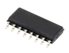
Analog Devices Inc.The MAX987/MAX988/MAX991/MAX992/MAX995/MAX996 single/dual/quad micropower comparatorsfeature low-voltage operation and rail-to-rail inputs andoutputs. Their operating voltage ranges from +2.5V to+5.5V, making them ideal for both 3V and 5V systems.These comparators also operate with ±1.25V to ±2.75Vdual supplies. They consume only 48µA per comparatorwhile achieving a 120ns propagation delay.Input bias current is typically 1.0pA, and input offset voltageis typically 0.5mV. Internal hysteresis ensures cleanoutput switching, even with slow-moving input signals.The output stage's unique design limits supply-currentsurges while switching, virtually eliminating the supplyglitches typical of many other comparators. TheMAX987/MAX991/MAX995 have a push-pull outputstage that sinks as well as sources current. Large internaloutput drivers allow rail-to-rail output swing withloads up to 8mA. The MAX988/MAX992/MAX996 havean open-drain output stage that can be pulled beyondVCC to 6V (max) above VEE. These open-drain versionsare ideal for level translators and bipolar to single-endedconverters.The single MAX987/MAX988 are available in tiny 5-pinSC70 packages, while the dual MAX991/MAX992 areavailable in ultra-small µMAX® package.ApplicationsDigital-Line ReceiversGround/Supply SensingIR ReceiversLevel TranslatorsMobile CommunicationsPortable Battery-Powered SystemsThreshold DetectorsWindow ComparatorsZero-Crossing Detectors
MAX998ESA+
Part Number : MAX998ESA+
Analog Devices Inc.The MAX976/MAX978/MAX998 dual/quad/single, high-speed, low-power comparators are optimized for +3V/+5V single-supply applications. They achieve a 20ns propagation delay while consuming only 225µA supply current per comparator. The MAX998 features a low-power shutdown mode that places the output in a high-impedance state and reduces supply current to 1nA.The MAX976/MAX978/MAX998 inputs have a common-mode voltage range that extends 200mV below ground. Their outputs are capable of rail-to-rail operation withoutexternal pullup circuitry, making these devices ideal for interface with CMOS/TTL logic. All inputs and outputs can tolerate a continuous short-circuit fault condition to either rail. The comparators' internal hysteresis ensures clean output switching, even with slow-moving input signals.For space-critical applications, the single MAX998 is available in a 6-pin SOT23 package, the dual MAX976 is available in an 8-pin µMAX® package, and the quad MAX978 is available in a 16-pin QSOP package.Applications3V SystemsBattery-Powered ApplicationsDigital-Line ReceiversIR ReceiversThreshold Detectors/Discriminators
DG212DY+
Part Number : DG212DY+
Analog Devices Inc.The DG202/DG212 are normally open, quad single-polesingle-throw (SPST) analog switches. TheseCMOS switches can be continuously operated withpower supplies ranging from ±4.5V to ±18V. Maximguarantees that these switches will not latch up if thepower supplies are disconnected with input signals stillconnected.The DG202/DG212 are similar to the DG201/DG211except for inverted control inputs. All devices haveguaranteed break-before-make switching, as well asessentially constant on-resistance over the analogsignal range. All switches conduct current in eitherdirection and add no offset to the output signal.Compared to the original manufacturer's products,Maxim's DG202/DG212 consume very little power,making them better suited for portable applications.Maxim has also eliminated the need for the third logicpower supply (VL) that is required for the operation ofthe original manufacturer's DG212 without sacrificingcompatibility.ApplicationsAnalog MultiplexersAutomatic Test EquipmentCommunication SystemsPBX, PABXProgrammable Gain AmplifiersSample/Holds
DG212ETE+T
Part Number : DG212ETE+T
Analog Devices Inc.The DG202/DG212 are normally open, quad single-polesingle-throw (SPST) analog switches. TheseCMOS switches can be continuously operated withpower supplies ranging from ±4.5V to ±18V. Maximguarantees that these switches will not latch up if thepower supplies are disconnected with input signals stillconnected.The DG202/DG212 are similar to the DG201/DG211except for inverted control inputs. All devices haveguaranteed break-before-make switching, as well asessentially constant on-resistance over the analogsignal range. All switches conduct current in eitherdirection and add no offset to the output signal.Compared to the original manufacturer's products,Maxim's DG202/DG212 consume very little power,making them better suited for portable applications.Maxim has also eliminated the need for the third logicpower supply (VL) that is required for the operation ofthe original manufacturer's DG212 without sacrificingcompatibility.ApplicationsAnalog MultiplexersAutomatic Test EquipmentCommunication SystemsPBX, PABXProgrammable Gain AmplifiersSample/Holds
MAX488ECPA+
Part Number : MAX488ECPA+
Analog Devices Inc.The MAX481E, MAX483E, MAX485E, MAX487E-MAX491E, and MAX1487E are low-power transceivers forRS-485 and RS-422 communications in harsh environments.Each driver output and receiver input is protectedagainst ±15kV electro-static discharge (ESD) shocks,without latchup. These parts contain one driver and onereceiver. The MAX483E, MAX487E, MAX488E, andMAX489E feature reduced slew-rate drivers that minimizeEMI and reduce reflections caused by improperly terminatedcables, thus allowing error-free data transmissionup to 250kbps. The driver slew rates of the MAX481E,MAX485E, MAX490E, MAX491E, and MAX1487E are notlimited, allowing them to transmit up to 2.5Mbps.These transceivers draw as little as 120µA supply currentwhen unloaded or when fully loaded with disableddrivers (see Selector Guide). Additionally, the MAX481E,MAX483E, and MAX487E have a low-current shutdownmode in which they consume only 0.5µA. All parts operatefrom a single +5V supply.Drivers are short-circuit current limited, and are protectedagainst excessive power dissipation by thermal shutdowncircuitry that places their outputs into a high-impedancestate. The receiver input has a fail-safe feature that guaranteesa logic-high output if the input is open circuit.The MAX487E and MAX1487E feature quarter-unit-loadreceiver input impedance, allowing up to 128 transceiverson the bus. The MAX488E-MAX491E aredesigned for full-duplex communications, while theMAX481E, MAX483E, MAX485E, MAX487E, andMAX1487E are designed for half-duplex applications.For applications that are not ESD sensitive see the pinandfunction-compatible MAX481, MAX483, MAX485,MAX487-MAX491, and MAX1487.ApplicationsIndustrial-Control Local Area NetworksLevel TranslatorsLow-Power RS-422 TransceiversLow-Power RS-485 TransceiversTransceivers for EMI-Sensitive Applications
MAX489EESD+
Part Number : MAX489EESD+
Analog Devices Inc.The MAX481E, MAX483E, MAX485E, MAX487E-MAX491E, and MAX1487E are low-power transceivers forRS-485 and RS-422 communications in harsh environments.Each driver output and receiver input is protectedagainst ±15kV electro-static discharge (ESD) shocks,without latchup. These parts contain one driver and onereceiver. The MAX483E, MAX487E, MAX488E, andMAX489E feature reduced slew-rate drivers that minimizeEMI and reduce reflections caused by improperly terminatedcables, thus allowing error-free data transmissionup to 250kbps. The driver slew rates of the MAX481E,MAX485E, MAX490E, MAX491E, and MAX1487E are notlimited, allowing them to transmit up to 2.5Mbps.These transceivers draw as little as 120µA supply currentwhen unloaded or when fully loaded with disableddrivers (see Selector Guide). Additionally, the MAX481E,MAX483E, and MAX487E have a low-current shutdownmode in which they consume only 0.5µA. All parts operatefrom a single +5V supply.Drivers are short-circuit current limited, and are protectedagainst excessive power dissipation by thermal shutdowncircuitry that places their outputs into a high-impedancestate. The receiver input has a fail-safe feature that guaranteesa logic-high output if the input is open circuit.The MAX487E and MAX1487E feature quarter-unit-loadreceiver input impedance, allowing up to 128 transceiverson the bus. The MAX488E-MAX491E aredesigned for full-duplex communications, while theMAX481E, MAX483E, MAX485E, MAX487E, andMAX1487E are designed for half-duplex applications.For applications that are not ESD sensitive see the pinandfunction-compatible MAX481, MAX483, MAX485,MAX487-MAX491, and MAX1487.ApplicationsIndustrial-Control Local Area NetworksLevel TranslatorsLow-Power RS-422 TransceiversLow-Power RS-485 TransceiversTransceivers for EMI-Sensitive Applications
MAX489EESD+T
Part Number : MAX489EESD+T
Analog Devices Inc.The MAX481E, MAX483E, MAX485E, MAX487E-MAX491E, and MAX1487E are low-power transceivers forRS-485 and RS-422 communications in harsh environments.Each driver output and receiver input is protectedagainst ±15kV electro-static discharge (ESD) shocks,without latchup. These parts contain one driver and onereceiver. The MAX483E, MAX487E, MAX488E, andMAX489E feature reduced slew-rate drivers that minimizeEMI and reduce reflections caused by improperly terminatedcables, thus allowing error-free data transmissionup to 250kbps. The driver slew rates of the MAX481E,MAX485E, MAX490E, MAX491E, and MAX1487E are notlimited, allowing them to transmit up to 2.5Mbps.These transceivers draw as little as 120µA supply currentwhen unloaded or when fully loaded with disableddrivers (see Selector Guide). Additionally, the MAX481E,MAX483E, and MAX487E have a low-current shutdownmode in which they consume only 0.5µA. All parts operatefrom a single +5V supply.Drivers are short-circuit current limited, and are protectedagainst excessive power dissipation by thermal shutdowncircuitry that places their outputs into a high-impedancestate. The receiver input has a fail-safe feature that guaranteesa logic-high output if the input is open circuit.The MAX487E and MAX1487E feature quarter-unit-loadreceiver input impedance, allowing up to 128 transceiverson the bus. The MAX488E-MAX491E aredesigned for full-duplex communications, while theMAX481E, MAX483E, MAX485E, MAX487E, andMAX1487E are designed for half-duplex applications.For applications that are not ESD sensitive see the pinandfunction-compatible MAX481, MAX483, MAX485,MAX487-MAX491, and MAX1487.ApplicationsIndustrial-Control Local Area NetworksLevel TranslatorsLow-Power RS-422 TransceiversLow-Power RS-485 TransceiversTransceivers for EMI-Sensitive Applications
MAX490ECSA+T
Part Number : MAX490ECSA+T
Analog Devices Inc.The MAX481E, MAX483E, MAX485E, MAX487E-MAX491E, and MAX1487E are low-power transceivers forRS-485 and RS-422 communications in harsh environments.Each driver output and receiver input is protectedagainst ±15kV electro-static discharge (ESD) shocks,without latchup. These parts contain one driver and onereceiver. The MAX483E, MAX487E, MAX488E, andMAX489E feature reduced slew-rate drivers that minimizeEMI and reduce reflections caused by improperly terminatedcables, thus allowing error-free data transmissionup to 250kbps. The driver slew rates of the MAX481E,MAX485E, MAX490E, MAX491E, and MAX1487E are notlimited, allowing them to transmit up to 2.5Mbps.These transceivers draw as little as 120µA supply currentwhen unloaded or when fully loaded with disableddrivers (see Selector Guide). Additionally, the MAX481E,MAX483E, and MAX487E have a low-current shutdownmode in which they consume only 0.5µA. All parts operatefrom a single +5V supply.Drivers are short-circuit current limited, and are protectedagainst excessive power dissipation by thermal shutdowncircuitry that places their outputs into a high-impedancestate. The receiver input has a fail-safe feature that guaranteesa logic-high output if the input is open circuit.The MAX487E and MAX1487E feature quarter-unit-loadreceiver input impedance, allowing up to 128 transceiverson the bus. The MAX488E-MAX491E aredesigned for full-duplex communications, while theMAX481E, MAX483E, MAX485E, MAX487E, andMAX1487E are designed for half-duplex applications.For applications that are not ESD sensitive see the pinandfunction-compatible MAX481, MAX483, MAX485,MAX487-MAX491, and MAX1487.ApplicationsIndustrial-Control Local Area NetworksLevel TranslatorsLow-Power RS-422 TransceiversLow-Power RS-485 TransceiversTransceivers for EMI-Sensitive Applications
MAX491EEPD+
Part Number : MAX491EEPD+
Analog Devices Inc.The MAX481E, MAX483E, MAX485E, MAX487E-MAX491E, and MAX1487E are low-power transceivers forRS-485 and RS-422 communications in harsh environments.Each driver output and receiver input is protectedagainst ±15kV electro-static discharge (ESD) shocks,without latchup. These parts contain one driver and onereceiver. The MAX483E, MAX487E, MAX488E, andMAX489E feature reduced slew-rate drivers that minimizeEMI and reduce reflections caused by improperly terminatedcables, thus allowing error-free data transmissionup to 250kbps. The driver slew rates of the MAX481E,MAX485E, MAX490E, MAX491E, and MAX1487E are notlimited, allowing them to transmit up to 2.5Mbps.These transceivers draw as little as 120µA supply currentwhen unloaded or when fully loaded with disableddrivers (see Selector Guide). Additionally, the MAX481E,MAX483E, and MAX487E have a low-current shutdownmode in which they consume only 0.5µA. All parts operatefrom a single +5V supply.Drivers are short-circuit current limited, and are protectedagainst excessive power dissipation by thermal shutdowncircuitry that places their outputs into a high-impedancestate. The receiver input has a fail-safe feature that guaranteesa logic-high output if the input is open circuit.The MAX487E and MAX1487E feature quarter-unit-loadreceiver input impedance, allowing up to 128 transceiverson the bus. The MAX488E-MAX491E aredesigned for full-duplex communications, while theMAX481E, MAX483E, MAX485E, MAX487E, andMAX1487E are designed for half-duplex applications.For applications that are not ESD sensitive see the pinandfunction-compatible MAX481, MAX483, MAX485,MAX487-MAX491, and MAX1487.ApplicationsIndustrial-Control Local Area NetworksLevel TranslatorsLow-Power RS-422 TransceiversLow-Power RS-485 TransceiversTransceivers for EMI-Sensitive Applications
MAX492ESA+
Part Number : MAX492ESA+
Analog Devices Inc.The dual MAX492, quad MAX494, and single MAX495 operational amplifiers combine excellent DC accuracy with rail-to-rail operation at the input and output. Since the common-mode voltage extends from VCC to VEE, the devices can operate from either a single supply (+2.7V to +6V) or split supplies (±1.35V to ±3V). Each op amp requires less than 150µA supply current. Even with this low current, the op amps are capable of driving a 1kΩ load, and the input referred voltage noise is only 25nV/√Hz. In addition, these op amps can drive loads in excess of 1nF.The precision performance of the MAX492/MAX494/MAX495, combined with their wide input and output dynamic range, low-voltage single-supply operation, and very low supply current, makes them an ideal choice for battery-operated equipment and other low-voltage applications. The MAX492/MAX494/MAX495 are available in DIP and SO packages in the industry-standard op-amp pin configurations. The MAX495 is also available in the smallest 8-pin SO: the µMAX® package.ApplicationsBattery-Powered ApplicationsData AcquisitionLow-Voltage ApplicationsPortable EquipmentSignal Conditioning
MAX509ACAP+
Part Number : MAX509ACAP+
Analog Devices Inc.The MAX509/MAX510 are quad, serial-input, 8-bit voltage-output digital-to-analog converters (DACs). They operate with a single +5V supply or dual ±5V supplies. Internal, precision buffers swing rail-to-rail. The reference input range includes both supply rails.The MAX509 has four separate reference inputs, allowing each DAC's full-scale range to be set independently. 20-pin DIP, SSOP, and SO packages are available. The MAX510 is identical to the MAX509 except it has two reference inputs, each shared by two DACs. The MAX510 is housed in space-saving 16-pin DIP and SO packages.The serial interface is double-buffered: A 12-bit input shift register is followed by four 8-bit buffer registers and four 8-bit DAC registers. A 12-bit serial word is used to load data into each register. Both input and DAC registers can be updated independently or simultaneously with single software commands. Two additional asynchronous control pins provide simultaneous updating (active-low LDAC) or clearing (active-low CLR) of input and DAC registers.The interface is compatible with Microwire™ and SPI™/QSPI™. All digital inputs and outputs are TTL/CMOS compatible. A buffered data output provides for readback or daisy-chaining of serial devices.ApplicationsDigital AttenuatorDigital Gain and Offset ControlGeneral Purpose
MAX510BEPE+
Part Number : MAX510BEPE+
Analog Devices Inc.The MAX509/MAX510 are quad, serial-input, 8-bit voltage-output digital-to-analog converters (DACs). They operate with a single +5V supply or dual ±5V supplies. Internal, precision buffers swing rail-to-rail. The reference input range includes both supply rails.The MAX509 has four separate reference inputs, allowing each DAC's full-scale range to be set independently. 20-pin DIP, SSOP, and SO packages are available. The MAX510 is identical to the MAX509 except it has two reference inputs, each shared by two DACs. The MAX510 is housed in space-saving 16-pin DIP and SO packages.The serial interface is double-buffered: A 12-bit input shift register is followed by four 8-bit buffer registers and four 8-bit DAC registers. A 12-bit serial word is used to load data into each register. Both input and DAC registers can be updated independently or simultaneously with single software commands. Two additional asynchronous control pins provide simultaneous updating (active-low LDAC) or clearing (active-low CLR) of input and DAC registers.The interface is compatible with Microwire™ and SPI™/QSPI™. All digital inputs and outputs are TTL/CMOS compatible. A buffered data output provides for readback or daisy-chaining of serial devices.ApplicationsDigital AttenuatorDigital Gain and Offset ControlGeneral Purpose
MAX5160NEUA+T
Part Number : MAX5160NEUA+T
Analog Devices Inc.The MAX5160/MAX5161 linear-taper digital potentiometers perform the same function as a mechanical potentiometer or a variable resistor. They consist of a fixed resistor and a wiper contact with 32 tap points that are digitally controlled by three lines for the 8-pin MAX5160 or by two lines for the 6-pin MAX5161.These parts are ideal for applications requiring digitally controlled resistors. Three resistance values are available for each part type: 50kΩ,100kΩ, and 200kΩ. A nominal resistor temperature coefficient of 50ppm/°C end-to-end and only 5ppm/°C ratiometric makes the MAX5160 ideal for applications requiring a low-temperature-coefficient variable resistor, such as low-tempco, adjustable-gain circuit configurations.The MAX5160 is available in an 8-pin µMAX package, and the MAX5161 is available in a 6-pin SOT23 package. Both devices are guaranteed over the extended-industrial temperature range (-40°C to +85°C).ApplicationsLCD Screen AdjustmentMechanical Potentiometer ReplacementsVolume Control
MAX860ISA+T
Part Number : MAX860ISA+T
Analog Devices Inc.The MAX860/MAX861 charge-pump voltage converters invert input voltages ranging from +1.5V to +5.5V, or double input voltages ranging from +2.5V to +5.5V. Because of their high switching frequencies, these devices use only two small, low-cost capacitors. Their 50mA output makes switching regulators unnecessary, eliminating inductors and their associated cost, size, and EMI. Greater than 90% efficiency over most of the load-current range, combined with a typical operating current of only 200µA (MAX860), provides ideal performance for both battery-powered and board-level voltage-conversion applications.A frequency-control (FC) pin provides three switching-frequencies to optimize capacitor size and quiescent current and to prevent interference with sensitive circuitry. Each device has a unique set of three available frequencies. A shutdown (active-low SHDN) pin reduces current consumption to less than 1µA. The MAX860/MAX861 are suitable for use in applications where the ICL7660 and MAX660's switching frequencies are too low. The MAX860/MAX861 are available in 8-pin µMAX® and SO packages.ApplicationsHandheld Instruments (PDAs, Palmtops)Interface Power SuppliesMedical InstrumentsOperational Amplifier Power SuppliesPortable Computing
ADXL320JCP
Part Number : ADXL320JCP
Analog Devices Inc.The ADXL320 is a low cost, low power, complete dual-axis accelerometer with signal conditioned voltage outputs, which is all on a single monolithic IC. The product measures acceleration with a full-scale range of ±5g (typical). It can also measure both dynamic acceleration (vibration) and static acceleration (gravity)The ADXL320’s typical noise floor is 250 µg/√Hz, allowing signals below 2 mg to be resolved in tilt-sensing applications using narrow bandwidths (
DS1124U-25+
Part Number : DS1124U-25+
Analog Devices Inc.The DS1124 is an 8-bit programmable timing element similar in function to the DS1021-25. The 256-delay intervals are programmed by using a 3-wire serial interface. With a 0.25ns step size, the DS1124 can provide a delay time from 20ns up to 84ns with an integral nonlinearity of ±3ns.ApplicationsDigital Test EquipmentDigital Video ProjectionLCD TelevisionsSignal Generators and AnalyzersTelecommunications
DS26518GN+
Part Number : DS26518GN+
Analog Devices Inc.The DS26518 is an 8-port framer and line interface unit (LIU) combination for T1, E1, J1 applications. Each port is independently configurable, supporting both long-haul and short-haul lines. The DS26518 Single-Chip Transceiver (SCT) is software and pinout compatible with the 4-port DS26514. It is nearly software compatible with the DS26528 and its derivatives.ApplicationsChannel BanksChannel Service Units (CSUs)Data Service Units (DSUs)MuxesRoutersSwitchesT1/E1 Test Equipment
DS4412U+
Part Number : DS4412U+
Analog Devices Inc.The DS4412 contains two I²C adjustable-current DACs that are each capable of sinking or sourcing current. Each output has 15 sink and 15 source settings that are programmed by I²C interface. The full-scale range and step size of each output is determined by an external resistor that can adjust the output current over a 4:1 range.The output pins, OUT0 and OUT1, power-up in a high-impedance state.ApplicationsAdjustable Current Sink or SourcePower-Supply AdjustmentPower-Supply Margining
LT1939EDD#PBF
Part Number : LT1939EDD#PBF
Analog Devices Inc.The LT1939 is a current mode PWM step-down DC/DC converter with an internal 2.3A switch. The wide input range of 3V to 25V makes the LT1939 suitable for regulating power from a wide variety of sources, including automotive batteries, industrial supplies and unregulated wall adapters.Resistor-programmable 250kHz to 2.2MHz frequency range and synchronization capability enable optimization between efficiency and external component size. Cycle-by-cycle current limit, frequency foldback and thermal shutdown provide protection against a shorted output. The soft-start feature controls the ramp rate of the output voltage, eliminating input current surge during start-up, and also provides output tracking.The LT1939 contains an internal NPN transistor with feedback control which can be configured as a linear regulator or as a linear regulator controller.The LT1939’s low current shutdown mode (
LT3009ESC8-2.5#TRPBF
Part Number : LT3009ESC8-2.5#TRPBF
Analog Devices Inc.The LT3009 Series are micropower, low dropout voltage (LDO) linear regulators. The devices supply 20mA output current with a dropout voltage of 280mV. No-load quiescent current is 3μA. Ground pin current remains at less than 5% of output current as load increases. In shutdown, quiescent current is less than 1μA. The LT3009 regulators optimize stability and transient response with low ESR ceramic capacitors, requiring a minimum of only 1μF. The regulators do not require the . addition of ESR as is common with other regulators. Internal protection circuitry includes current limiting, thermal limiting, reverse-battery protection and reverse-current protection.The LT3009 Series are ideal for applications that require moderate output drive capability coupled with ultralow standby power consumption. The device is available in fixed output voltages of 1.2V, 1.5V, 1.8V, 2.5V, 3.3V and 5V, and as an adjustable device with an output voltage range down to the 600mV reference. The LT3009 is available in the 6-lead DFN and 8-lead SC70 packages.Applications Low Current Battery-Powered Systems Keep-Alive Power Supplies Remote Monitoring Utility Meters Hotel Door Locks


